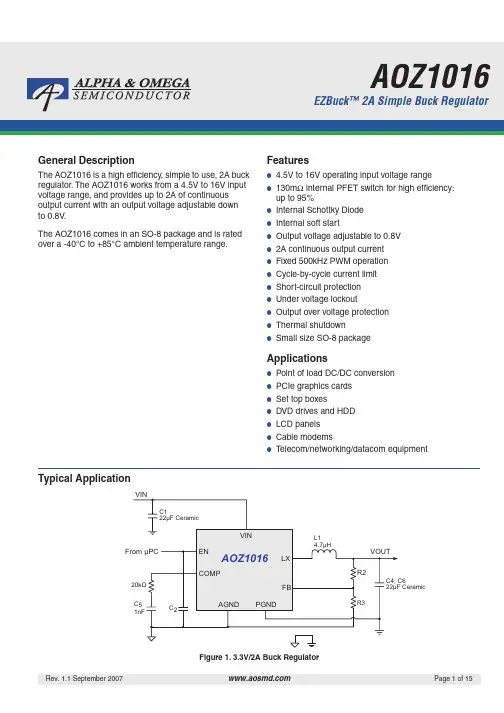
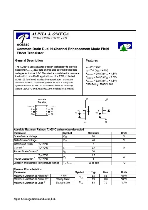
AO660_datasheet
- 格式:docx
- 大小:661.96 KB
- 文档页数:8
AO6601Complementary Enhancement Mode Field Effect TransistorD1 D2G1S1 S2AO6601n-channel MOSFET Electrical Characteristics (T J=25°C unless otherwise noted)A: The value of RθJA is measured with the device mounted on 1in2FR-4 board with 2oz. Copper, in a still air environment with T A=25°C. The value in any given application depends on the user's specific board design. The current rating is based on the t≤ 10s thermal resistance rating.B: Repetitive rating, pulse width limited by junction temperature.C. The R θJA is the sum of the thermal impedence from junction to lead RθJL and lead to ambient.D. The static characteristics in Figures 1 to 6 are obtained using 80∝s pulses, duty cycle 0.5% max.E. These tests are performed with the device mounted on 1 in2FR-4 board with 2oz. Copper, in a still air environment with T A=25°C. The SOA curve provides a single pulse rating.Rev 3 : June 2005THIS PRODUCT HAS BEEN DESIGNED AND QUALIFIED FOR THE CONSUMER MARKET. APPLICATIONS OR USES AS CRITICAL COMPONENTS IN LIFE SUPPORT DEVICES OR SYSTEMS ARE NOT AUTHORIZED. AOS DOES NOT ASSUME ANY LIABILITY ARISING OUT OF SUCH APPLICATIONS OR USES OF ITS PRODUCTS. AOS RESERVES THE RIGHT TO IMPROVE PRODUCT DESIGN, FUNCTIONS AND RELIABILITY WITHOUT NOTICE.AO6601 n-channel typical characteristicsTYPICAL ELECTRICAL AND THERMAL CHARACTERISTICS15 10V101294.5V3V8V DS =5V6 25°C125°C6 3 0 2.5VV GS =2V12345V DS (Volts)Fig 1: On-Region Characteristics4 21.8 1.6 00.511.522.533.5V GS (Volts)Figure 2: Transfer CharacteristicsV GS =4.5V1.4V GS =10V750 0246810I D (A)Figure 3: On-Resistance vs. Drain Current and GateVoltage1.210.8V GS =2.5V0 255075100125150175Temperature (°C)Figure 4: On-Resistance vs. Junction Temperature200 150 1.0E+01 1.0E+00I D =2A1.0E-01125°C100125°C1.0E-02 1.0E-035025°C25°C1.0E-040 0246810V GS (Volts)Figure 5: On-Resistance vs. Gate-Source Voltage1.0E-050.00.2 0.4 0.6 0.8 1.0 1.2V SD (Volts)Figure 6: Body-Diode CharacteristicsV GS =2.5VV GS =4.5VV GS =10VAlpha and Omega Semiconductor, Ltd.I D (A ) I D (A )R D S (O N )(m Ω)I S (A ) N o r m a l i z e d O n -R e s i s t a n c e R D S (O N )(m Ω)AO6601 n-channel typical characteristicsTYPICAL ELECTRICAL AND THERMAL CHARACTERISTICS5V DS =15V 6004 I D =3.4A5003 2 1 0 0123456Q g (nC)Figure 7: Gate-Charge Characteristics400 300 200 100 0 C issC ossC rss51015202530V DS (Volts)Figure 8: Capacitance Characteristics 100.010.0 1.0R DS(ON)limited1s 10sT J(Max)=150°C T A =25°C10∝s100∝s 1ms0.1s 10ms2015 105T J(Max)=150°C T A =25°C0.1 DC0.1110 100V DS (Volts)Figure 9: Maximum Forward Biased SafeOperating Area (Note E)0.0010.01 0.1 1 10 100 1000Pulse Width (s)Figure 10: Single Pulse Power Rating Junction-to-Ambient (Note E)1010.1D=T on /TT J,PK =T A +P DM .Z θJA .R θJA R θJA =110°C/W In descending orderD=0.5, 0.3, 0.1, 0.05, 0.02, 0.01, single pulseP DT onSingle Pulse0.010.000010.00010.0010.010.1110 100 1000Pulse Width (s)Figure 11: Normalized Maximum Transient Thermal ImpedanceTV G S (V o l t s )C a p a c i t a n c e (p F )P o w e r (W )Z θJ A N o r m a l i z e d T r a n s i e n t T h e r m a l R e s i s t a n c eI D (A m p s )AO6601p-channel MOSFET Electrical Characteristics (T J=25°C unless otherwise noted)A: The value of RθJA is measured with the device mounted on 1in2FR-4 board with 2oz. Copper, in a still air environment with T A=25°C. The value in any given application depends on the user's specific board design. The current rating is based on the t≤ 10s thermal resistance rating. B: Repetitive rating, pulse width limited by junction temperature.C. The R θJA is the sum of the thermal impedence from junction to lead RθJL and lead to ambient.D. The static characteristics in Figures 1 to 6,12,14 are obtained using 80∝s pulses, duty cycle 0.5% max.E. These tests are performed with the device mounted on 1 in2FR-4 board with 2oz. Copper, in a still air environment with T A=25°C. The SOA curve provides a single pulse rating.Rev 3 : June 2005THIS PRODUCT HAS BEEN DESIGNED AND QUALIFIED FOR THE CONSUMER MARKET. APPLICATIONS OR USES AS CRITICAL COMPONENTS IN LIFE SUPPORT DEVICES OR SYSTEMS ARE NOT AUTHORIZED. AOS DOES NOT ASSUME ANY LIABILITY ARISING OUT OF SUCH APPLICATIONS OR USES OF ITS PRODUCTS. AOS RESERVES THE RIGHT TO IMPROVE PRODUCT DESIGN, FUNCTIONS AND RELIABILITY WITHOUT NOTICE.AO6601, AO6601LP-CHANNEL: TYPICAL ELECTRICAL AND THERMAL CHARACTERISTICS2015-10V-5V-4.5V -4V108 V DS =-5V25°C1050 V GS =-3.5V-3V-2.5V-2V12345-V DS (Volts)Fig 1: On-Region CharacteristicsV GS =-2.5V6420 1.61.4 1.2 125°C0.511.522.533.54-V GS (Volts)Figure 2: Transfer CharacteristicsV GS =-4.5V, V GS =-10VV GS =-2.5VI D =-2A1501234 5 6-I D (A)Figure 3: On-Resistance vs. Drain Current and GateVoltage0.8 025 50 75 100 125 150 175Temperature (°C)Figure 4: On-Resistance vs. Junction Temperature350 1.0E+01 1.0E+001.0E-01 125°C1.0E-02 1.0E-0325°C246810-V GS (Volts)Figure 5: On-Resistance vs. Gate-Source Voltage1.0E-04 1.0E-05 1.0E-060.00.2 0.4 0.6 0.8 1.0 1.2-V SD (Volts)Figure 6: Body-Diode CharacteristicsV GS =-4.5VV =-10VI D =-2A125°C25°C-I D (A )-I D (A )R D S (O N )(m Ω)-I S (A )N o r m a l i z e d O n -R e s i s t a n c eR D S (O N )(m Ω)AO6601 p-channel typical characteristicsTYPICAL ELECTRICAL AND THERMAL CHARACTERISTICS5V DS =-15V 6004 3 2 1 0 I D =-2.0A123456-Q g (nC)Figure 7: Gate-Charge Characteristics500 400 300 200 100 0 C issC ossC rss51015202530-V DS (Volts)Figure 8: Capacitance Characteristics 100.010.01.0T J(Max)=150°C T A =25°CR DS(ON) limited0.1s1s10s10∝s 100∝s 1ms10ms2015105T J(Max)=150°C T A =25°C0.1 DC0.1110100-V DS (Volts)Figure 9: Maximum Forward Biased SafeOperating Area (Note E)0.0010.01 0.1 1 10 100 1000Pulse Width (s)Figure 10: Single Pulse Power Rating Junction-to-Ambient (Note E)1010.1D=T on /TT J,PK =T A +P DM .Z θJA .R θJA R θJA =110°C/W In descending orderD=0.5, 0.3, 0.1, 0.05, 0.02, 0.01, single pulseP DT onSingle Pulse0.010.000010.00010.0010.010.1110 100 1000Pulse Width (s)Figure 11: Normalized Maximum Transient Thermal ImpedanceT-V G S (V o l t s )C a p a c i t a n c e (p F )P o w e r (W )Z θJ A N o r m a l i z e d T r a n s i e n t T h e r m a l R e s i s t a n c e-I D (A m p s )。