Using the Serial Peripheral Interface (SPI)
- 格式:pdf
- 大小:149.71 KB
- 文档页数:11

Product Reference ManualSKU: ABX00083DescriptionThe Arduino Nano ESP32 (with and without headers) is a Nano form factor board based on the ESP32-S3 (embedded in the NORA-W106-10B from u-blox®). This is the first Arduino board to be based fully on an ESP32, and features Wi-Fi®, Bluetooth® LE, debugging via native USB in the Arduino IDE as well as low power.The Nano ESP32 is compatible with the Arduino IoT Cloud, and has support for MicroPython. It is an ideal board for getting started with IoT development.Target areas:Maker, Debugging, IoT, MicroPythonFeaturesXtensa® Dual-core 32-bit LX7 Microprocessor Up to 240 MHz384 kB ROM512 kB SRAM16 kB SRAM in RTC (low power mode)DMA ControllerPowerOperating voltage 3.3 VVUSB supplies 5 V via USB-C® connectorVIN range is 6-21 VConnectivityWi-Fi®Bluetooth® LEBuilt-in antenna2.4 GHz transmitter/receiverUp to 150 MbpsPins14x digital (21x including analog)8x analog (available in RTC mode)SPI(D11,D12,D13), I2C (A4/A5), UART(D0/D1) Communication PortsSPII2CI2SUARTCAN (TWAI®)Low Power7 μA consumption in deep sleep mode240 μA consumption in light sleep modeRTC MemoryUltra Low Power (ULP) CoprocessorPower Management Unit (PMU)ADC in RTC mode55556778888999910101011111111121212131313131314151516Contents1 The Board1.1 Application Examples 2 ESP32 Core3 Recommended Operating Conditions4 Block Diagram5 Board Topology5.1 Front View6 NORA-W106-10B (Radio Module / MCU)6.1 Xtensa® Dual-Core 32bit LX7 Microprocessor 6.2 Wi-Fi®6.3 Bluetooth®7 System7.1 Resets 7.2 Timers 7.3 Interrupts8 Serial Communication Protocols8.1 Inter-Integrated Circuit (I2C)8.2 Inter-IC Sound (I2S)8.3 Serial Peripheral Interface (SPI)8.4 Universal Asynchronous Receiver/Transmitter (UART)8.5 Two Wire Automotive Interface (TWAI®)9 External Flash Memory 10 USB Connector 11 Power Options11.1 Power Tree 11.2 Pin Voltage 11.3 VIN Rating 11.4 VUSB11.5 Using the 3.3 V Pin 11.6 Pin Current 12 Pinout12.1 Analog (JP1)12.2 Digital (JP2)13 Mounting Holes And Board Outline161617171717174191920202014 Board Operation14.1 Getting Started - IDE14.2 Getting Started - Arduino Web Editor 14.3 Getting Started - Arduino IoT Cloud 14.4 Online Resources 14.5 Board Recovery15 Declaration of Conformity CE DoC (EU)16 Declaration of Conformity to EU RoHS & REACH 211 01/19/202117 Conflict Minerals Declaration 18 FCC Caution19 Company Information 20 Reference Documentation 21 Change Log1 The BoardNano ESP32 is a 3.3 V development board based on the NORA-W106-10B from u-blox®, a module that includes a ESP32-S3 system on a chip (SoC). This module has support for Wi-Fi® and Bluetooth® Low Energy (LE), with amplified communication through a built-in antenna. The CPU (32-bit Xtensa® LX7) support clock frequencies at up to 240 MHz and has native support for debugging via the USB-C® connector.1.1 Application ExamplesHome automation: an ideal board for automating your home, and can be used for smart switches, automatic lighting and motor control for e.g. motor controlled blinds.IoT sensors: with several dedicated ADC channels, accessible I2C/SPI buses and a robust ESP32-S3 based radio module, this board can easily be deployed to monitor sensor values.Low power designs: create battery powered applications with low power consumption, utilising the built in low power modes of the ESP32-S3 SoC.2 ESP32 CoreThe Nano ESP32 uses the Arduino Core for ESP32 boards, a derivation of Espressif's arduino-esp32 core. Rating3 Recommended Operating ConditionsSymbol Description Min Typ Max UnitV IN Input voltage from VIN pad67.021VV USB Input voltage from USB connector 4.8 5.0 5.5VT OP Operating Temperature-402585°CFunctional Overview4 Block DiagramArduino Nano ESP32 Block Diagram5 Board Topology5.1 Front ViewTop View of Arduino Nano ESP32 Ref.DescriptionM1NORA-W106-10B (ESP32-S3 SoC)J1CX90B-16P USB-C® connectorJP11x15 analog headerJP21x15 digital headerU2MP2322GQH step down converterU3GD25B128EWIGR 128 Mbit (16 MB) ext. flash memory DL1RGB LEDDL2LED SCK (serial clock)DL3LED Power (green)D2PMEG6020AELRX Schottky DiodeD3PRTR5V0U2X,215 ESD Protection6 NORA-W106-10B (Radio Module / MCU)The Nano ESP32 features the NORA-W106-10B stand alone radio module, embedding an ESP32-S3 series SoC as well as an embedded antenna. The ESP32-S3 is based on an Xtensa® LX7 series microprocessor.6.1 Xtensa® Dual-Core 32bit LX7 MicroprocessorThe microprocessor for the ESP32-S3 SoC inside the NORA-W106 module is a dual-core 32-bit Xtensa® LX7. Each core can run at up to 240 MHz and has 512 kB SRAM memory. The LX7 features:32-bit customized instruction set128-bit data bus32-bit multiplier / dividerSupport for JTAG debuggingThe LX7 has a 384 kB ROM (Read Only Memory), and 512 kB of SRAM (Static Random Access Memory). It also features an 8 kB RTC FAST and RTC SLOW memory. These memories are designed for low-power operations, where the SLOW memory can be accessed by the ULP (Ulta Low Power) coprocessor, retaining the data in deep sleep mode.6.2 Wi-Fi®The NORA-W106-10B module supports the Wi-Fi® 4 IEEE 802.11 standards b/g/n, with an output power EIRP at up to 10 dBm. The max range for this module is 500 meters.802.11b: 11 Mbit/s802.11g: 54 Mbit/s802.11n: 72 Mbit/s max at HT-20 (20 MHz), 150 Mbit/s max at HT-40 (40 MHz)6.3 Bluetooth®The NORA-W106-10B module supports Bluetooth® LE v5.0 with an output power EIRP at up to 10 dBm and data rates up to 2 Mbps. It has the option to scan and advertise simultaneously, as well as supporting multiple connections in peripheral/central mode.7 System7.1 ResetsThe ESP32-S3 has support for four levels of reset:CPU: resets CPU0/CPU1 coreCore: resets the digital system, except for the RTC peripherals (ULP coprocessor, RTC memory).System: resets the entire digital system, including the RTC peripherals.Chip: resets the entire chip.It is possible to conduct a software reset of this board, as well as obtaining the reset reason.To do a hardware reset of the board, use the onboard reset button (PB1).7.2 TimersThe Nano ESP32 has the following timers:52-bit system timer with 2x 52-bit counters (16 MHz) and 3x comparators.4x general-purpose 54-bit timers3x watchdog timers, two in main system (MWDT0/1), one in the RTC module (RWDT).7.3 InterruptsAll GPIOs on the Nano ESP32 can be configured to be used as interrupts, and is provided by an interrupt matrix. Interrupt pins are configured on an application level, using the following configurations:LOWHIGHCHANGEFALLINGRISING8 Serial Communication ProtocolsThe ESP32-S3 chip provides flexibility for the various serial protocols it supports. For example, the I2C bus can be assigned to almost any available GPIO.8.1 Inter-Integrated Circuit (I2C)Default pins:A4 - SDAA5 - SCLThe I2C bus is by default assigned to the A4/A5 (SDA/SCL) pins for retro compatibility. This pin assignment can however be changed, due to the flexibility of the ESP32-S3 chip.The SDA and SCL pins can be assigned to most GPIOs, however some of these pins may have other essential functions that prevents I2C operations to run successfully.Please note: many software libraries uses the standard pin assignment (A4/A5).8.2 Inter-IC Sound (I2S)There two I2S controllers that are typically used for communication with audio devices. There are no specific pins assigned for I2S, this can be used by any free GPIO.Using standard or TDM mode, the following lines are used:MCLK - master clockBCLK - bit clockWS - word selectDIN/DOUT - serial dataUsing PDM mode:CLK - PDM clockDIN/DOUT serial dataRead more about the I2S protocol in Espressif's Peripheral API - InterIC Sounds (I2S)8.3 Serial Peripheral Interface (SPI)SCK - D13COPI - D12CIPO - D11CS - D10The SPI controller is by default assigned to the pins above.8.4 Universal Asynchronous Receiver/Transmitter (UART)D0 / TXD1 / RXThe UART controller is by default assigned to the the pins above.8.5 Two Wire Automotive Interface (TWAI®)The CAN/TWAI® controller is used to communicate with systems using the CAN/TWAI® protocol, particularly common in the automotive industry. There are no specific pins assigned for the CAN/TWAI® controller, any free GPIO can be used.Please note: TWAI® is also known as the CAN2.0B, or "CAN classic". The CAN controller is NOT compatible with CAN FD frames.9 External Flash MemoryNano ESP32 features a 128 Mbit (16 MB) external flash, the GD25B128EWIGR (U3). This memory is connected to the ESP32 via Quad Serial Peripheral Interface (QSPI).The operating frequency for this IC is 133 MHz, and has a data transfer rate at up to 664 Mbit/s.10 USB ConnectorThe Nano ESP32 has one USB-C® port, used to power and program your board as well as sending & receiving serial communication.Note that you should not power the board with more than 5 V via the USB-C® port.11 Power OptionsPower can either be supplied via the VIN pin, or via USB-C® connector. Any voltage input either via USB or VIN is stepped down to 3.3 V using the MP2322GQH (U2) converter.The operating voltage for this board is 3.3 V. Please note that there's no 5V pin available on this board, only the VBUS can provide 5 V when the board is powered via USB.11.1 Power TreeArduino Nano ESP32 power tree.11.2 Pin VoltageAll digital & analog pins on the Nano ESP32 are 3.3 V. Do not connect any higher voltage devices to any of the pins as it will risk damaging the board.11.3 VIN RatingThe recommended input voltage range is 6-21 V.You should not attempt to power the board with a voltage outside the recommended range, particularly not higher than 21 V.The efficiency of the converter depends on the input voltage via the VIN pin. See the average below for a board operation with normal current consumption:4.5 V - >90%.12 V - 85-90%18 V - <85%This information is extracted from the MP2322GQH's datasheet.11.4 VUSBThere is no 5V pin available on the Nano ESP32. 5 V can only be provided via the VUSB, which is supplied directly from the USB-C® power source.While powering the board via the VIN pin, the VUSB pin is not activated. This means you have no option of providing 5 V from the board unless powered via USB or externally.11.5 Using the 3.3 V PinThe 3.3 V pin is connected to the 3.3 V rail which is connected to the output of the MP2322GQH step down converter. This pin is primarily used to power external components.11.6 Pin CurrentThe GPIOs on the Nano ESP32 can handle source currents up to 40 mA, and sink currents up to 28 mA. Never connect devices that draw higher current directly to a GPIO.Mechanical Information12 PinoutPinout for Nano ESP32.12.1 Analog (JP1)Pin Function Type Description1SCK NC Serial Clock2+3V3Power+3V3 Power Rail3BOOT0Mode Board Reset 04A0Analog Analog input 05A1Analog Analog input 16A2Analog Analog input 27A3Analog Analog input 38A4Analog Analog input 4 / I²C Serial Datal (SDA) 9A5Analog Analog input 5 / I²C Serial Clock (SCL) 10A6Analog Analog input 611A7Analog Analog input 712VUSB Power USB power (5V)13BOOT1Mode Board Reset 114GND Power Ground15VIN Power Voltage Input12.2 Digital (JP2)Pin Function Type Description1D12 / CIPO*Digital Controller In Peripheral Out2D11 / COPI*Digital Controller Out Peripheral In3D10Digital Chip Select4D9Digital GPIO 95D8Digital GPIO 86D7Digital GPIO 77D6Digital GPIO 68D5Digital GPIO 59D4Digital GPIO 410D3Digital GPIO 311D2Digital GPIO 212GND Power Ground13RST Internal Reset14D1/RX Digital GPIO 4 / Serial 0 Receiver (RX) 15D0/TX Digital GPIO 3 / Serial 0 Transmitter (TX) *CIPO/COPI replaces the MISO/MOSI terminology.13 Mounting Holes And Board OutlineMechanical View of Nano ESP3214 Board Operation14.1 Getting Started - IDEIf you want to program your Nano ESP32 while offline you need to install the Arduino IDE [1]. To connect the Nano ESP32 to your computer, you will need a Type-C® USB cable, which can also provide power to the board, as indicated by the LED (DL1).14.2 Getting Started - Arduino Web EditorAll Arduino boards, including this one, work out-of-the-box on the Arduino Web Editor [2], by just installing a simple plugin.The Arduino Web Editor is hosted online, therefore it will always be up-to-date with the latest features and support for all boards. Follow [3] to start coding on the browser and upload your sketches onto your board.14.3 Getting Started - Arduino IoT CloudAll Arduino IoT enabled products are supported on Arduino IoT Cloud which allows you to log, graph and analyze sensor data, trigger events, and automate your home or business.14.4 Online ResourcesNow that you have gone through the basics of what you can do with the board you can explore the endless possibilities it provides by checking exciting projects on Arduino Project Hub [4], the Arduino Library Reference [5], and the online store [6]; where you will be able to complement your board with sensors, actuators and more. 14.5 Board RecoveryAll Arduino boards have a built-in bootloader which allows flashing the board via USB. In case a sketch locks up the processor and the board is not reachable anymore via USB, it is possible to enter bootloader mode by double-tapping the reset button right after the power-up.Certifications15 Declaration of Conformity CE DoC (EU)We declare under our sole responsibility that the products above are in conformity with the essential requirements of the following EU Directives and therefore qualify for free movement within markets comprising the European Union (EU) and European Economic Area (EEA).16 Declaration of Conformity to EU RoHS & REACH 21101/19/2021Arduino boards are in compliance with RoHS 2 Directive 2011/65/EU of the European Parliament and RoHS 3 Directive 2015/863/EU of the Council of 4 June 2015 on the restriction of the use of certain hazardous substances in electrical and electronic equipment.Substance Maximum Limit (ppm)Lead (Pb)1000Cadmium (Cd)100Mercury (Hg)1000Hexavalent Chromium (Cr6+)1000Poly Brominated Biphenyls (PBB)1000Poly Brominated Diphenyl ethers (PBDE)1000Bis(2-Ethylhexyl} phthalate (DEHP)1000Benzyl butyl phthalate (BBP)1000Dibutyl phthalate (DBP)1000Diisobutyl phthalate (DIBP)1000Exemptions : No exemptions are claimed.Arduino Boards are fully compliant with the related requirements of European Union Regulation (EC) 1907 /2006 concerning the Registration, Evaluation, Authorization and Restriction of Chemicals (REACH). We declare none of the SVHCs (https://echa.europa.eu/web/guest/candidate-list-table), the Candidate List of Substances of Very High Concern for authorization currently released by ECHA, is present in all products (and also package) in quantities totaling in a concentration equal or above 0.1%. To the best of our knowledge, we also declare that our products do not contain any of the substances listed on the "Authorization List" (Annex XIV of the REACH regulations) and Substances of Very High Concern (SVHC) in any significant amounts as specified by the Annex XVII of Candidate list published by ECHA (European Chemical Agency) 1907 /2006/EC.17 Conflict Minerals DeclarationAs a global supplier of electronic and electrical components, Arduino is aware of our obligations with regards to laws and regulations regarding Conflict Minerals, specifically the Dodd-Frank Wall Street Reform and Consumer Protection Act, Section 1502. Arduino does not directly source or process conflict minerals such as Tin, Tantalum, Tungsten, or Gold. Conflict minerals are contained in our products in the form of solder, or as a component in metal alloys. As part of our reasonable due diligence Arduino has contacted component suppliers within our supply chain to verify their continued compliance with the regulations. Based on the information received thus far we declare that our products contain Conflict Minerals sourced from conflict-free areas.18 FCC CautionAny Changes or modifications not expressly approved by the party responsible for compliance could void the user’s authority to operate the equipment.This device complies with part 15 of the FCC Rules. Operation is subject to the following two conditions:(1) This device may not cause harmful interference(2) this device must accept any interference received, including interference that may cause undesired operation. FCC RF Radiation Exposure Statement:1. This Transmitter must not be co-located or operating in conjunction with any other antenna or transmitter.2. This equipment complies with RF radiation exposure limits set forth for an uncontrolled environment.3. This equipment should be installed and operated with a minimum distance of 20 cm between the radiator &your body.English: User manuals for licence-exempt radio apparatus shall contain the following or equivalent notice in a conspicuous location in the user manual or alternatively on the device or both. This device complies with Industry Canada licence-exempt RSS standard(s). Operation is subject to the following two conditions:(1) this device may not cause interference(2) this device must accept any interference, including interference that may cause undesired operation of the device.French: Le présent appareil est conforme aux CNR d’Industrie Canada applicables aux appareils radio exempts de licence. L’exploitation est autorisée aux deux conditions suivantes :(1) l’ appareil nedoit pas produire de brouillage(2) l’utilisateur de l’appareil doit accepter tout brouillage radioélectrique subi, même si le brouillage est susceptible d’en compromettre le fonctionnement.IC SAR Warning:English This equipment should be installed and operated with a minimum distance of 20 cm between the radiator and your body.French: Lors de l’ installation et de l’ exploitation de ce dispositif, la distance entre le radiateur et le corps est d ’au moins 20 cm.Important: The operating temperature of the EUT can’t exceed 85℃ and shouldn’t be lower than -40 ℃. Hereby, Arduino S.r.l. declares that this product is in compliance with essential requirements and other relevant provisions of Directive 201453/EU. This product is allowed to be used in all EU member states.19 Company InformationCompany name Arduino SRLCompany Address Via Andrea Appiani, 25 - 20900 MONZA Italy)20 Reference DocumentationRef LinkArduino IDE (Desktop)https:///en/Main/SoftwareArduino Web Editor(Cloud)https:///editorWeb Editor - Getting Started https:///cloud/web-editor/tutorials/getting-started/getting-started-web-editorProject Hub https:///projecthub?by=part&part_id=11332&sort=trending Library Reference https:///arduino-libraries/Online Store https:///21 Change LogDate Changes08/06/2023Release。
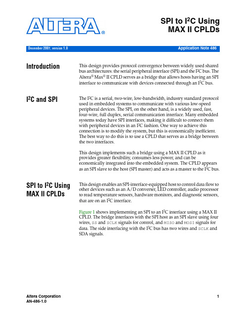
Application Note 486SPI to I 2C Using MAX II CPLDs IntroductionThis design provides protocol convergence between widely used shared bus architectures: the serial peripheral interface (SPI) and the I 2C bus. The Altera ® Max ® II CPLD serves as a bridge that allows hosts having an SPI interface to communicate with devices connected through an I 2C bus.I 2C and SPIThe I 2C is a serial, two-wire, low-bandwidth, industry standard protocol used in embedded systems to communicate with various low-speed peripheral devices. The SPI, on the other hand, is a widely used, fast, four-wire, full duplex, serial communication interface. Many embedded systems today have SPI interfaces, making it difficult to connect them with peripheral devices in an I 2C fashion. One way to achieve this connection is to modify the system, but this is economically inefficient. The best way to do this is to use a CPLD that serves as a bridge between the two interfaces.This design implements such a bridge using a MAX II CPLD as it provides greater flexibility, consumes less power, and can be economically integrated into the embedded system. The CPLD appears as an SPI slave to the host (SPI master) and acts as a master to the I 2C bus.SPI to I 2C UsingMAX II CPLDsThis design enables an SPI-interface-equipped host to control data flow to other devices such as an A/D converter, LED controller, audio processor to read temperature sensors, hardware monitors, and diagnostic sensors, that are on an I 2C interface.Figure 1 shows implementing an SPI to an I 2C interface using a MAX II CPLD. The bridge interfaces with the SPI host as an SPI slave using four wires, SS and SCLK signals for control, and MISO and MOSI signals for data. The side interfacing with the I 2C bus has two wires and SCLK and SDA signals.December 2007, version 1.0Figure1.Implementing an SPI to I2C Interface Using a MAX II CPLDSPI InterfaceThe SPI bus normally has only one master and many slaves connected toit. The CPLD bridge acts as one of the slaves to the SPI master device.Figure2 shows the SPI timing diagram. Table1 shows the SPI interfacepin descriptions.Figure2.SPI Timing DiagramThe SPI host sends:■command register (8 bit)■data in (8 bit)The SPI host receives:■status register (8 bit)■data out (8 bit)The SPI word length is fixed at 16 bits. CPOL =0 and CPHA =1, as indicated in Figure 2. In every SPI word, the command register dictates the functions on the I 2C bus and the data in holds the data to be sent by the I 2C bus. Similarly, the last bit of the status register is the acknowledge bit and the data out is the data received over the I 2C line in the previous I 2C cycle.At the end of every SPI bus, the slave select line goes high, indicating a word complete and, per the value of command register at that time, an I 2C bus cycle is executed. After a fixed delay, depending on the frequency of the I 2C SCL, another SPI word can be sent. The minimum delay between two SPI words is the I 2C SCL clock frequency.Table 1.SPI Interface Pin DescriptionsSignal Purpose Direction SS Slave select Input (active low)SCLK SPI clock Input MISO Master-in Slave-out Output MOSI Master-out Slave-in OutputI 2C Interface The CPLD bridge acts as a master to the I 2C bus. Since the purpose of this design is to provide an interface between an SPI master and an I 2C slave device, multi-master support is not provided on the I 2C bus. Table 2 shows the I 2C interface pin descriptions.The I 2C functions are carried out based on the command register value received from the SPI side. The significance of the value stored in the command register is shown in Table 3.The data read in a particular I 2C transaction is stored in the data out register and is read by the SPI master in its next SPI transaction. The last command word, 00000000 (b), is required for the SPI master to read the value of status and data out registers without doing anything on the I 2C bus. The I 2C command format is shown in Figure 3.Figure 3.I 2C Command Format Table 2.I 2C Interface Pin Descriptions Signal Purpose Direction SCLK I 2C serial clock Output SDA I 2C data bus Bidirectional Table 3.I 2C Commands Command Register Purpose on the I 2C Line Data In Register 10000000Start/repeat start Slave address + R/W 01000000Write a byteData to be written 00100000Read a byte Don’t care 00010000Stop Don’t care 00000000Null, wait state Don’t careImplementationThis design can be implemented with an EPM240 or any other MAX II CPLD. Implementation involves using this design source code and allocating the appropriate signal and control lines to the general purpse I/O (GPIO) lines of the MAX II CPLD. An SPI master and an I 2C slave are additional resources required to demonstrate this implementation.The following steps detail the demonstration using the MDN-B2 board, a PC parallel-port-based SPI environment created using Freescale’s SPIGen software (along with suitable parallel port interfacing hardware), and an I 2C slave battery gauge module (supplied with the MDN-B2).Table 4 shows the EPM240G pin assignments.1Unused pins are assigned as input tri-stated in the Quartus ® II software’s device and pin option settings. SPI_sclk is assigned a 2.5-V Schmitt Trigger input in the I/O standards column in the Quartus II software during pin assignment. The Assignment Editor in the Quartus II software is used to enable Auto Open Drain on the I2C_scl and I2C_sda pins. Compile the design after turning on the appropriate settings.Design Notes To demonstrate this design on the MDN-B2 demo board, complete the following:1.To set up the SPI environment using a PC and its parallel port, download SPI emulation software such as the SPIGen from Freescale. This software is available for free download after accepting Freescale’s terms and conditions of use and free registration. Table 4.EPM240G Pin Assignments Pin Assignments Signal Pin I2C_scl :Pin 39I2C_sda Pin 40SPI_cs Pin 95SPI_miso Pin 91SPI_mosi Pin 92SPI_clk Pin 96f Visit the following website to download the SPI emulation software:/files/soft_dev_tools/software/device_drivers/SPIGen.html2.Once you register, download and install SPIGen. You will need toconfigure it to suit your application and work with theParallelport-to-SPI dongle that is provided with the MDN-B2 demoboard.3.Open the SPIGen software and click the Configure menu. SelectEdit Configuration. In the General tab, verify the default PortAddress is the correct port address of the parallel port in your PC. Ifit is not, select the correct option. You can find your PC’s parallelport address by looking at the settings in Control Panel > System >Hardware > Device Manager > Ports > ECP Printer Port (LPT1) >Resources.Figure4 shows the demo arrangement.Figure4.Demo Arrangement4.Select a 16-bit format and choose to display the SPI values inhexadecimal (Intel-Format) file (.hex) format.5.Configure the SPI Pins tab by completing the following:a.Leave the pin assignments in their default settings (ChipSelect:2, Data In: 3, Data Out: 12, and Clock: 4).b.Leave Bit Order in its default MSB is sent first setting.c.Change Chip Select to High when asserted.d.Change Data In and Data out to Low = 1.e.Change the SPI Type to Type 4.f.Click Apply and OK to return to the main SPIGen screen.6.Connect the Parallelport-to-SPI dongle to the parallel port of yourPC. Use a parallel port extension cable to make it more convenient to connect the dongle to the demo board. The parallel-port-based SPI environment is now ready to use.7.Turn on the power to the demo board (using slide switch SW1).Download the design to the MAX II CPLD through the JTAG header JP5 on the demo board and a conventional programming cable(ByteBlaster™II or USB-Blaster™).8.Keep SW4 on the demo board pressed before and during the start ofthe programming process. Once complete, turn off the power and remove the JTAG connector.9.Mount the DS2745 I2C battery gauge module (provided with theMDN-B2 demo board) on JP3 of the demo board. Ensure the redmark on the module matches pin#1 on JP3.10.Connect the Parallelport-to-SPI dongle to the demo board.11.Connect the 6-pin connector on the dongle’s pigtail wire to the JP8on the demo board. Ensure the red wire on this 6-pin connectormatches pin#2 on JP8.1Note that JP8 is a 10x2 pin header; this 6-pin connector will only occupy a portion of JP8.12.Turn on the demo board using slide switch SW1.13.Table5 indicates the sequence of the .hex data to send using theWord to Send (DI) field in the SPIGen software.Table5.SPI “Data to Send” in Hex Using SPIGen (Part 1 of2)Signal Direction Command/DataSend (DI)80 90 (start + slave address)Send (DI)40 0C (write + memory addr)Receive (DO)01 00 (ack)Send (DI)80 91 (start + slave address)e the .hex data from Table 5 and click Send Once each time you want to send the SPI data. Verify the acknowledgment data is received.15.Observe the battery gauge data received. It is received in two parts, giving the MSB 8-bits data first and the LSB 3-bit data next (last row).16.Vary the yellow preset on the battery gauge module and observe the varying data received. The yellow preset varies the input voltage to the battery gauge chip (Maxim DS2745) which provides the voltage readings through its I 2C interface and in 11-bit 2’s complement form. fFor more information, refer to:/quick_view2.cfm/qv_pk/4994Source CodeThis design has been implemented in Verilog and successful operation has been demonstrated using the MDN-B2 demo board, as referenced in the documentation. The source code, testbench, and complete Quartus II project are available at:/literature/an/an486_design_example.zip ConclusionAs illustrated by this design, MAX II CPLDs are a great choice to implement industry standard interfaces such as the SPI and I 2C. Their low power, easy power sequencing, and internal oscillator make them ideal programmable logic devices to implement interface converter applications such as the SPI to I 2C.Receive (DO)01 00 (ack)Send (DI)20 00 (read)Receive (DO)01 ?? (ack + MSB data)Send (DI)00 00 (do nothing)Receive (DO)01 ?? (ack + LSB data)Table 5.SPI “Data to Send” in Hex Using SPIGen (Part 2 of 2)Signal Direction Command/DataReferenced Documents This application note references the following documents:■/literature/an/an486_design_example.zip ■/files/soft_dev_tools/software/device_dri vers/SPIGen.html■/quick_view2.cfm/qv_pk/4994Additional Resources The following are additional resources for this application note:■MAX II CPLD home page:/products/devices/cpld/max2/mx2-index.jsp■MAX II Device Literature page:http://www.altera.-com/literature/lit-max2.jsp■MAX II Power-Down Designs:/support/examples/max/exm-power-down.html■MAX II Application Notes:AN 428: MAX II CPLD Design GuidelinesAN 422: Power Management in Portable Systems Using MAX II CPLDsDocumentRevision HistoryTable6 shows the revision history for this application note.Table6.Document Revision HistoryDate and DocumentVersionChanges Made Summary of ChangesDecember 2007,v1.0Initial release.—101 Innovation DriveSan Jose, CA 95134 Technical Support: /support Literature Services: literature@ Copyright © 2007 Altera Corporation. All rights reserved. Altera, The Programmable Solutions Company, the stylized Altera logo, specific device designations, and all other words and logos that are identified as trademarks and/or service marks are, unless noted otherwise, the trademarks and service marks of Altera Corporation in the U.S. and other countries. All other product or service names are the property of their re-spective holders. Altera products are protected under numerous U.S. and foreign patents and pending applications, maskwork rights, and copyrights. Altera warrants performance of its semiconductor products to current specifications in accordance with Altera's standard warranty, but reserves the right to make chang-es to any products and services at any time without notice. Altera assumes no responsibility or liability arising out of the application or use of any information, product, or service describedherein except as expressly agreed to in writing by Altera Corporation. Altera customersare advised to obtain the latest version of device specifications before relying on any pub-lished information and before placing orders for products or services.。
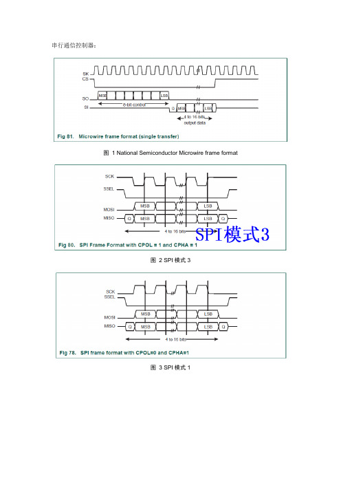
串行通信控制器:图 1 National Semiconductor Microwire frame format图 2 SPI模式3图 3 SPI模式1图 4 SPI模式2图 5 SPI模式0图 6 4-wire Texas Instruments synchronous图 3 ATMEL 9200 SSC用作IIS图 4 ATMEL 9200 SSC用作SPIATMEL 9200 SSC 如果可以灵活配置可用作SPI、IIC、IIS、SSI 、National Semiconductor Microwire frame format、SSP究SPI接口时,引申出来的SSP;在网上居然没有找到完整的协议规范文档;只好东拼西凑(多数内容来于博文),但还是没搞明白在硬件上如何兼容其他类型的总线,这种兼容有什么好处?A Synchronous Serial Port (SSP) is a controller that supports the Serial Peripheral Interface (SPI), 4-wire Synchronous Serial Interface (SSI), and Microwire serial buses. A SSP uses a master-slave paradigm to communicate across its connected bus.支持MOTO Master SPI, TI Synchronous Serial Interface(SSI),1-bit,4-bit,8-bit SD/SDIO/MMC, CE-ATAand 1-bit, 4-bit MS. 5大类的工作模式,使之成为一个小强般的强大.这个port的设计目的是为了和i2c,可移动多媒体控制和通信.SSP还加强了spi模式以支持1-bit的legacy MMC Card.SSP还支持SPI,SSI的slave操作SSP有一个专用的DMA通道,可以被CPU&PIO直接控制.SSP有11个external pins,SSP_SCK, SSP_CMD, SSP_DATA[7:0], and SSP_DETECT.不同的组合定义了不同的模式bit rate是由SSPCLK分出来的,分频的reg是clcok_divide,从2到254.还有个类似功能的寄存器,叫clock_rate, 值是从1到256.于是我们有了SSP_CLK=SSPCLK/(clcok_divide*(1+clock_rate));搞成一个reg不就可以了,两个8bit的,和一个9bit的不是一回事.....SSP, SSI的Frame Format每个data format长4到16个bit,是programmable的,MSB first when sending,有两种frame type可以被选,1 moto SPI, 地球人都知道spi是moto定义的.2 TI SSI这两种format,SSP_SCK都是无效的,当SSP idle,只有发数据或收数据的时候,SSP_SCK才会toggle. SSP_SCLK的idle状态是用来表明一个接受timeout的,这个情况发生在接收fifo还有数据在一个timeout周期之后.对于SPI的frame format,在整个传输中,serial frame(SSn)是低的,被拉低的.对于SSI的frame format,ssn pin有个一周期的pulse,在clock的上升沿发出,提前于每个传输的frame. 并且规定了,任何SSP,片外的slave都必须在SSP_SCK的rising edge驱动数据,对方会latch数据在faling edge.那么下面开始具体的讲解这些不同的模式spispi被用在inter-component通信和1-bit的mmc card中spi dma模式SPI是一个双工双向的接口.但是很多应用只需要半双工的数据传输.这颗芯片里面有一个单独的channel给SSP,可以被配置成收或发,在DMA收模式中,spi会连续的发送data reg里面的数据,而在发模式,输入会被ignore.spi的frame formatspi是个四线接口,SSn切换到slave选择上.spi的format主要是inactive state和SSP_SCK的phase可以被配置.被配置是通过两个寄存器来实现的.1 clock polarity0会导致一个steady-state low值在ssp_sck pin上1的时候如果data没有被传输,那么一个steady-state的一个high值会在ssp_sck上2clock phase0数据在第一个时钟沿被capture1数据在第二个时钟沿被capture,这里说的时钟沿是包括上升沿和下降沿.通过这两个1bit的寄存器,spi有4种不同的工作方式,下面挨着详细讲解.(1)polarity=0,phase=0idle被定义为ssp_sck force to low;ssn force to high;output MOSI(最后字母是I,但是功能那,output,呵呵.) force to low;if master mode, ssp_sck 是output,反之input定义了idle后,定义下工作条件,发fifo中已经有数据.ssn拉低后,传输开始.slave的input信号MISO会立即enable,MOSI也会被使能.半个周期后,有效的master数据已经摆在输出MOSI上面,现在来看master和slave的数据都有效了,master的ssp_sck在又一个半周期后,开始变高.data就会在上升沿被capture,并且下降沿propagate.如果是single word的传输,当所有data被传输后,ssn在最后一个数据被capture后一周期就又变回高,idle了撒如果是连续的back-to-back传输,ssn必须有个pulse是被拉高的,具体操作类似上面的single word.这是因为phase为0时,slave select pin会freeze data.所以需要ssn 变化一下来解决这个问题.(2)polarity=0,phase=1idle的定义和上面一样唯一不同的是data就会被下降沿capture,并且上升沿propagate(3)polarity=1,phase=0对于idle的定义,唯一的区别是ssp_sck force to high并且由于这点区别,sck先有failing edge,导致了,data就会被下降沿capture,并且上升沿propagate (4)polarity=1,phase=1idle的定义没变由于phase=1了,第二个时钟沿开始work,于是data就会在上升沿被capture,并且下降沿propagate.。

SPI(SerialPeripheralInterface)协议SPI是串⾏外设接⼝(Serial Peripheral Interface)的缩写,是Motorola推出的⼀种同步串⾏接⼝技术,是⼀种⾼速的、全双⼯、同步的通信总线。
全双⼯:host能与外围从设备之间的发送线和接收线各⾃独⽴,能同时进⾏发送数据和接收数据。
源同步传输⽂章内容SPI介绍SPI协议通信时序详解SPI数据传输⽅式SPI总线优缺点1、SPI介绍应⽤场景SPI协议主要⽤于短距离的通信系统中,特别是嵌⼊式系统:存储器:RAM,EEPROM,Flash等数模转换器:A/D, D/A转换器等驱动接⼝:LED显⽰驱动器,I/O接⼝芯⽚,UART接收器等。
主从模式控制:SPI以主从⽅式进⾏⼯作,这种模式通常包含⼀个master和⼀个或多个slave,需要⾄少4根线(在单向传输时3根也可以),分别为:SDO/MOSI(master output slave input):主设备数据输出,从设备数据输⼊;SDI/MISO(master input slave output):主设备数据输⼊,从设备数据输出;SCLK:时钟信号,由主设备产⽣;CS/SS:⽚选信号,主设备控制并⽤于选择与其通信的从设备。
多Slave的SPI协议SPI协议可以操作在⼀个master对应⼀个或者多个slave的条件下,此时有多个CS/SS⽚选信号,但是⼀个时间只能有⼀个⽚选信号有效。
slave的输出端⼝MISO都是三态驱动;⾼电平,低电平和不选中时输出为⾼阻态。
数据交换(data exchanges)SPI设备之间的数据传输称为数据交换⽽不是数据传输。
这是因为SPI设备不能在进⾏数据通信的过程中仅充当transmitter和recieiver的⾓⾊,⽽是在每个时钟周期内,主从SPI设备都会发送1bit⼤⼩的数据,相当于主从设备进⾏了1bit的数据交换。
在数据的传输过程中,每次接收到的数据必须在下⼀次数据传输之前被采样,如果之前接收的数据没有被采样,那么这些已经收到的数据可能被丢弃,导致 SPI 模块最终失效,因此,在程序中,⼀般都会在 SPI 传输完数据之后,去读取 SPI 设备⾥⾯的数据,即使这些数据是在我们程序中是没有⽤的。

SPII2CUART三种串行总线的原理区别及应用SPI(Serial Peripheral Interface),I2C(Inter-Integrated Circuit)和UART(Universal Asynchronous Receiver/Transmitter)是常见的串行总线通信协议,它们在嵌入式系统中被广泛使用。
以下是对这三种串行总线的原理、区别及应用的详细介绍。
1. SPI(Serial Peripheral Interface)SPI是一种同步的、全双工的串行总线协议,通常由一个主设备和一个或多个从设备组成。
SPI总线上通信是基于时钟信号进行同步的,主设备产生时钟信号,从设备在时钟的边沿上发送和接收数据。
在SPI总线上,主设备控制通信的起始和结束,并通过片选信号选择与之通信的从设备。
SPI总线上的数据传输是基于多线制的,其中包括主设备的时钟线(SCLK)、数据输出线(MOSI)、数据输入线(MISO)和片选线(SS)。
SPI总线具有以下特点:-速度较快,可以达到十几MHz甚至上百MHz的传输速率。
-支持多主设备,但每个时刻只能有一个主设备处于活动状态。
-适用于短距离通信,通常在PCB上的芯片之间进行通信。
-数据传输可靠性较高。
SPI总线广泛应用于各种设备之间的数据传输,例如存储器、传感器、显示模块等。
2. I2C(Inter-Integrated Circuit)I2C也是一种同步的、双向的串行总线协议,由一个主设备和一个或多个从设备组成。
I2C总线上的通信也是基于时钟信号进行同步的,主设备产生时钟信号和开始/停止条件,从设备在时钟边沿上发送和接收数据。
I2C总线上的数据传输是基于两根线—串行数据线(SDA)和串行时钟线(SCL)。
I2C总线具有以下特点:- 通信速度较慢,大多数设备的传输速率为100kbps,但也支持高达3.4Mbps的快速模式。
-支持多主设备,可以同时连接多个主设备。
光伏发电逆变器毕业论文中英文资料外文翻译文献附录:文献翻译TMS320LF2407, TMS320LF2406, TMS320LF2402TMS320LC2406, TMS320LC2404, MS320LC2402DSP CONTROLLERSThe TMS320LF240x and TMS320LC240x devices, new members of the ‘24x family of digital signal processor (DSP) controllers, are part of the C2000 platform of fixed-point DSPs. The ‘240x devices offer the enhanced TMS320 architectural design of the ‘C2xx core CPU for low-cost, low-power, high-performance processing capabilities. Several advanced peripherals, optimized for digital motor and motion control applications, have been integrated to provide a true single chip DSP controller. While code-compatible with the existing ‘24x DSP controller devices, the ‘240x offers increased processing performance (30 MIPS) and a higher level of peripheral integration. See the TMS320x240x device summary section for device-specific features.The ‘240x family offers an array of memory sizes and different peripherals tailored to meet the specific price/performance points required by various applications. Flash-based devices of up to 32K words offer a reprogrammable solution useful for:◆Applications requiring field programmability upgrades.◆Development and initial prototyping of applications that migrate to ROM-baseddevices.Flash devices and corresponding ROM devices are fully pin-to-pin compatible. Note that flash-based devices contain a 256-word boot ROM to facilitate in-circuit programming.All ‘240x devices offer at least one event manager module which has been optimized for digital motor control and power conversion applications. Capabilities of this module include centered- and/or edge-aligned PWM generation, programmable deadband to prevent shoot-through faults, and synchronized analog-to-digital conversion. Devices with dual event managers enable multiple motor and/or converter control with a single ‗240x DSP controller.The high performance, 10-bit analog-to-digital converter (ADC) has a minimum conversion time of 500 ns and offers up to 16 channels of analog input. The auto sequencing capability of the ADC allows a maximum of 16 conversions to take place in a single conversion session without any CPU overhead.A serial communications interface (SCI) is integrated on all devices to provide asynchronous communication to other devices in the system. For systems requiring additional communication interfaces; the ‘2407, ‘2406, and ‘2404 offer a 16-bit synchronous serial peripheral interface (SPI). The ‘2407 and ‘2406 offer a controller area network (CAN) communications module that meets 2.0B specifications. To maximize device flexibility, functional pins are also configurable as general purpose inputs/outputs (GPIO).To streamline development time, JTAG-compliant scan-based emulation has been integrated into all devices. This provides non-intrusive real-time capabilities required to debug digital control systems. A complete suite of code generation tools from C compilers to the industry-standard Code Composerdebugger supports this family. Numerous third party developers not only offer device-level development tools, but also system-level design and development support.PERIPHERALSThe integrated peripherals of the TMS320x240x are described in the following subsections:●Two event-manager modules (EV A, EVB)●Enhanced analog-to-digital converter (ADC) module●Controller area network (CAN) module●Serial communications interface (SCI) module●Serial peripheral interface (SPI) module●PLL-based clock module●Digital I/O and shared pin functions●External memory interfaces (‘LF2407 only)●Watchdog (WD) timer moduleEvent manager modules (EV A, EVB)The event-manager modules include general-purpose (GP) timers, full-compare/PWM units, capture units, and quadrature-encoder pulse (QEP) circuits. EV A‘s and EVB‘s timers, compare units, and capture units function identically. However, timer/unit names differ for EV A and EVB. Table 1 shows the module and signal names used. Table 1 shows the features and functionality available for the event-manager modules and highlights EV A nomenclature.Event managers A and B have identical peripheral register sets with EV A starting at 7400h and EVB starting at 7500h. The paragraphs in this section describe the function of GP timers, compare units, capture units, and QEPs using EV A nomenclature. These paragraphs are applicable to EVB with regard to function—however, module/signal names would differ.Table 1. Module and Signal Names for EV A and EVBEVENT MANAGER MODULESEV AMODULESIGNALEVBMODULESIGNALGP Timers Timer 1Timer 2T1PWM/T1CMPT2PWM/T2CMPTimer 3Timer 4T3PWM/T3CMPT4PWM/T4CMPCompare Units Compare 1Compare 2Compare 3PWM1/2PWM3/4PWM5/6Compare 4Compare 5Compare 6PWM7/8PWM9/10PWM11/12Capture Units Capture 1Capture 2Capture 3CAP1CAP2CAP3Capture 4Capture 5Capture 6CAP4CAP5CAP6QEP QEP1QEP2QEP1QEP2QEP3QEP4QEP3QEP4External Inputs DirectionExternalClockTDIRATCLKINADirectionExternal ClockTDIRBTCLKINBGeneral-purpose (GP) timersThere are two GP timers: The GP timer x (x = 1 or 2 for EV A; x = 3 or 4 for EVB) includes:● A 16-bit timer, up-/down-counter, TxCNT, for reads or writes● A 16-bit timer-compare register, TxCMPR (double-buffered with shadow register), forreads or writes● A 16-bit timer-period register, TxPR (double-buffered with shadow register), forreads or writes● A 16-bit timer-control register,TxCON, for reads or writes●Selectable internal or external input clocks● A programmable prescaler for internal or external clock inputs●Control and interrupt logic, for four maskable interrupts: underflow, overflow, timercompare, and period interrupts● A selectable direction input pin (TDIR) (to count up or down when directionalup-/down-count mode is selected)The GP timers can be operated independently or synchronized with each other. The compare register associated with each GP timer can be used for compare function and PWM-waveform generation. There are three continuous modes of operations for each GP timer in up- or up/down-counting operations. Internal or external input clocks with programmable prescaler are used for each GP timer. GP timers also provide the time base for the other event-manager submodules: GP timer 1 for all the compares and PWM circuits, GP timer 2/1 for the capture units and the quadrature-pulse counting operations. Double-buffering of the period and compare registers allows programmable change of the timer (PWM) period and the compare/PWM pulse width as needed.Full-compare unitsThere are three full-compare units on each event manager. These compare units use GP timer1 as the time base and generate six outputs for compare and PWM-waveform generation using programmable deadband circuit. The state of each of the six outputs is configured independently. The compare registers of the compare units are double-buffered, allowing programmable change of the compare/PWM pulse widths as needed.Programmable deadband generatorThe deadband generator circuit includes three 8-bit counters and an 8-bit compare register. Desired deadband values (from 0 to 24 µs) can be programmed into the compare register for the outputs of the three compare units. The deadband generation can be enabled/disabled for each compare unit output individually. The deadband-generator circuit produces two outputs (with orwithout deadband zone) for each compare unit output signal. The output states of the deadband generator are configurable and changeable as needed by way of the double-buffered ACTR register.PWM waveform generationUp to eight PWM waveforms (outputs) can be generated simultaneously by each event manager: three independent pairs (six outputs) by the three full-compare units with programmable deadbands, and two independent PWMs by the GP-timer compares.PWM characteristicsCharacteristics of the PWMs are as follows:●16-bit registers●Programmable deadband for the PWM output pairs, from 0 to 24 µs●Minimum deadband width of 50 ns●Change of the PWM carrier frequency for PWM frequency wobbling as needed●Change of the PWM pulse widths within and after each PWM period as needed●External-maskable power and drive-protection interrupts●Pulse-pattern-generator circuit, for programmable generation of asymmetric,symmetric, and four-space vector PWM waveforms●Minimized CPU overhead using auto-reload of the compare and period registersCapture unitThe capture unit provides a logging function for different events or transitions. The values of the GP timer 2 counter are captured and stored in the two-level-deep FIFO stacks when selected transitions are detected on capture input pins, CAPx (x = 1, 2, or 3 for EV A; and x = 4, 5, or 6 for EVB). The capture unit consists of three capture circuits.Capture units include the following features:●One 16-bit capture control register, CAPCON (R/W)●One 16-bit capture FIFO status register, CAPFIFO (eight MSBs are read-only, eightLSBs are write-only)●Selection of GP timer 2 as the time base●Three 16-bit 2-level-deep FIFO stacks, one for each capture unit●Three Schmitt-triggered capture input pins (CAP1, CAP2, and CAP3)—one input pinper capture unit. [All inputs are synchronized with the device (CPU) clock. In order fora transition to be captured, the input must hold at its current level to meet two risingedges of the device clock. The input pins CAP1 and CAP2 can also be used as QEPinputs to the QEP circuit.]●User-specified transition (rising edge, falling edge, or both edges) detection●Three maskable interrupt flags, one for each capture unitEnhanced analog-to-digital converter (ADC) moduleA simplified functional block diagram of the ADC module is shown in Figure 1. The ADC module consists of a 10-bit ADC with a built-in sample-and-hold (S/H) circuit. Functions of the ADC module include:●10-bit ADC core with built-in S/H●Fast conversion time (S/H + Conversion) of 500 ns●16-channel, muxed inputs●Autosequencing capability provides up to 16 ―autoconversions‖ in a single session.Each conversion can be programmed to select any 1 of 16 input channels●Sequencer can be operated as two independent 8-state sequencers or as one large16-state sequencer (i.e., two cascaded 8-state sequencers)●Sixteen result registers (individually addressable) to store conversion values●Multiple triggers as sources for the start-of-conversion (SOC) sequence✧S/W – software immediate start✧EV A – Event manager A (multiple event sources within EV A)✧EVB – Event manager B (multiple event sources within EVB)✧Ext – External pin (ADCSOC)●Flexible interrupt control allows interrupt request on every end of sequence (EOS) orevery other EOS●Sequencer can operate in ―start/stop‖ mode, allowing multiple ―time-sequencedtriggers‖ to synchronize conv ersions●EV A and EVB triggers can operate independently in dual-sequencer mode●Sample-and-hold (S/H) acquisition time window has separate prescale control●Built-in calibration mode●Built-in self-test modeThe ADC module in the ‘240x has been enhanced to pro vide flexible interface to event managers A and B. The ADC interface is built around a fast, 10-bit ADC module with total conversion time of 500 ns (S/H + conversion). The ADC module has 16 channels, configurable as two independent 8-channel modules to service event managers A and B. The two independent 8-channel modules can be cascaded to form a 16-channel module. Figure 2 shows the block diagram of the ‘240x ADC module.The two 8-channel modules have the capability to autosequence a series of conversions,each module has the choice of selecting any one of the respective eight channels available through an analog mux. In the cascaded mode, the autosequencer functions as a single 16-channel sequencer. On each sequencer, once the conversion is complete, the selected channel value is stored in its respective RESULT register. Autosequencing allows the system to convert the same channel multiple times, allowing the user to perform oversampling algorithms. This gives increased resolution over traditional single-sampled conversion results.Figure 2. Block Diagram of the ‘240x ADC ModuleFrom TMS320LF2407, TMS320LF2406, TMS320LF2402TMS320LC2406, TMS320LC2404, MS320LC2402数字信号处理控制器TMS320LF240x和TMS320LC240x系列芯片作为’24x系列DSP控制器的新成员,是C2000平台下的一种定点DSP芯片。
AN970/08021/10AN970APPLICATION NOTESPI COMMUNICATION BETWEEN ST7 AND EEPROMby 8-Bit Micro Application TeamINTRODUCTIONThe goal of this application note is to present a practical example of communication using the SPI peripheral of the ST7.It shows an easy way of communicating between a ST7 microcontroller and a M95xxx SPI EEPROM. The purpose is to perform, through SPI, a write in the memory, followed by a read of the written data.1SPI COMMUNICATION BETWEEN ST7 AND EEPROM1 ST7 / EEPROM SPI INTERFACEThis section summarizes the main features of the ST7/EEPROM SPI interface. Please refer to the ST7 datasheet for more details.The Serial Peripheral Interface (SPI) allows full-duplex, synchronous, serial communication between devices. A SPI system may consist of a master and several slaves, or of a system in which devices may be either master or slave.There is only one master at any one time.The Bus signals are:- The serial clock (SCK).- The MOSI (Master Out Slave In).- The MISO (Master In Slave Out).One more pin, the SS pin (slave select), is needed to select the slave or the master mode for each device. this can be done in hardware or software mode.In this application the ST7 is always used as master (SS pin = high level) and configures the EEPROM mode through an output. The ST7 and SPI interface set-up is shown Figure 1.During SPI transfer, data is simultaneously transmitted (shifted out serially) and received (shifted in serially). Data are transmitted MSB first. The serial clock is used to synchronize the data transfer during a sequence of eight clock pulses.Figure 1. ST7 and SPI Interface Set-UpST7SPI InterfaceEEPROMSSSCK MOSI MISO S VCCI/OC QD M95040SPI COMMUNICATION BETWEEN ST7 AND EEPROM 2 ST72264 CONFIGURATION2.1 I/O CONTROLFour pins of the ST72264 are used:- The 3 data and clock SPI pins (SCK, MOSI, MISO).- An output pin to select and deselect the M95xxx.- SS pin to select master or slave mode.In our application, the output for selecting the M95xxx is pin 3 of Port B. It is configured as output push-pull (refer to the datasheet for details).2.2 SPI PERIPHERAL2.2.1 GeneralThis peripheral is configured with the SPI Control Register.70SPIE SPE SPR2MSTR CPOL CPHA SPR1SPR0The output must be enabled (SPE = 1).If the SS pin is high (see SPICSR), the ST72264 can be declared as master by setting the MSTR bit.The transmission speed, in master mode, is selected using the SPR0, SPR1 and SPR2 bits. The CPOL and CPHA bits define the timing characteristics.When the SPIE bit is set, SPI interrupts are enabled (not used in our case).2.2.2 SS software configurationThe SS pin can be fixed by hardware, either connected to Vss (for a slave configuration) or to Vdd (for a master configuration). But it can also be software driven through the SPICSR reg-ister (SSM and SSI bits) :70SPIF WCOL OVR MODF-SOD SSM SSITo set the master configuration (as in our case) : SSM=1 and SSI=1To set the slave configuration: SSM=1 and SSI=0SPI COMMUNICATION BETWEEN ST7 AND EEPROM2.2.3 Baud ratesFirst the communication speed must be chosen. As the clock is given by the master, the user has to configure the baud rate of the ST7 SPI (SPR[2-0] bits in the SPICR register).For each CPU frequency, six Baud Rates are available. If f CPU= 8MHz, the baud rate range is 62.5kHz to 2MHz.2.2.4 Clock phase and polarityThen the clock polarity and the clock phase have to be chosen.The clock polarity (CPOL bit of the SPCR register) controls the steady state value of the clock when no data is being transferred.The clock phase (CPHA bit of the SPCR register) selects on which clock transition the bit cap-ture is made and consequently on which clock transition data is latched.The user must be careful of the fact that some devices do not allow all timing relationships. For instance, the ST95040 EEPROM device accepts only CPOL,CPHA = (0,0) or (1,1) configura-tions.SPI COMMUNICATION BETWEEN ST7 AND EEPROM 3 M95040 EEPROM MANAGEMENT AND CONFIGURATION3.1 MAIN FEATURESThis is a 4K memory composed of two pages of 2K bytes.All instructions, addresses and data are shifted in and out of the chip MSB first.The write protect pin (W) and the hold pin (H) are not used in our application (both are high level).3.2 STATUS REGISTERThis device has one status register.The BP1 and BP0 bits in the status register can be used to write protect a block of memory. In this application, both bits are cleared, allowing write access to all the memory.The WEL bit indicates the status of the write enable latch.The WIP bit indicates whether the memory is busy with a write operation.3.3 INSTRUCTION SETPrior to any operation, the device must be selected (SS pin at low level), then an one-byte in-struction code must be sent to the EEPROM. The device has a set of 6 instructions (see Table 1 Instruction Set).Table 1. Instruction SetInstruction Description Instruction formatWREN Set Write Enable Latch0000 0110WRDI Reset Write Enable Latch0000 0100RDSR Read Status Register0000 0101WRSR Write Status Register0000 0001READ Read Data from Memory Array0000 A8011WRITE Write Data to Memory Array0000 A8010Notes: A8 = 1, Upper page selected.A8 = 0, Lower page selected.SPI COMMUNICATION BETWEEN ST7 AND EEPROM4 ST7 / EEPROM SPI PROTOCOLThe use of the main functions are briefly described below. For a complete description of the protocol, please refer to the M95040 SPI EEPROM data sheet.Write_enable: The memory contains a write enable latch. This latch must be set prior to any WRITE or WRSR operation.Byte_write: This function will write up to 16 bytes of data in the EEPROM. After the WRITE in-struction, the memory address must be specified before sending data.Byte_read: This function reads the memory. After the READ instruction, the memory address is specified. To be able to send the data, the EEPROM must receive the clock from the master: the ST7. This is made by sending a dummy byte. This operation will generate the 8 clock bits needed. The dummy value will not be seen by the EEPROM.Write_SR: Give the proper value to the Status Register prior to any communication.Read_SR: This process is similar to the byte read process. It will be used to check if there is a write in progress (WIP bit of the status register).5 SPI COMMUNICATION BETWEEN AN ST7 AND AN EEPROMThe software included with this application note is only the SPI driver. The complete software can be found in the software library in the ST internet website. It is of course only an example. It is up to the user to adapt it to his specific application.5.1 GENERAL DESCRIPTIONThe software is a polling SPI communication between the ST72264 and EEPROM.The first part of the software performs to the initialization of the ST72264 (core and SPI periph-eral) and of the EEPROM (value of status register for no protection).Then it executes the write cycles. The «write_loop» writes in the EEPROM (16 bytes at a time for optimization), the values 0 to 111 from the address 0 up to 111.The third part executes the read cycles. The «read_loop» reads the content of the EEPROM at a time from address 0 up to 111.Finally, the software ends in an infinite loop.SPI COMMUNICATION BETWEEN ST7 AND EEPROM5.2 HARDWARE DESCRIPTIONTwo components were used for the application:- 1 ST72264 MCU - 1 M95040 EEPROMFigure 2. Hardware descriptionSS pin of ST72264 is software driven (high state for a master device).The SCK pin is connected to the serial clock pin (C) of the E²PROMs.The MOSI pin to the serial input pins (D).The MISO pin to the serial output pins (Q).S pin of the EEPROM is connected to the PB3 output pin of ST72264.5.3 FLOWCHARTSThe flowchart of the application is presented below (Figure 3).Q DS V CC V SSC W H ST72264110pFM95040V CCV CC V SSV CC V SS1V CC V SSSS (soft driven)SCK PB3MISO MOSI V CCSPI COMMUNICATION BETWEEN ST7 AND EEPROMFigure 3. Flowchart: MAINMAIN initialization write_enable byte_write read_SRwrite in progress?increment address A by 16X at address A end of writing?(x=111)clear X and A byte_read at address A increment Xend of reading?(x=111)ENDclear X and A yes nononoyes yesSPI COMMUNICATION BETWEEN ST7 AND EEPROM5.4 USE OF SEVERAL EEPROMSIt is possible to communicate with several EEPROMs. Each one is selected in turn. Then the same protocol as described before is followed.The main point is to reserve one I/O pin to select each device.A hardware schematic using two devices is given below (Figure 4).The selection of the devices is made using the PB2 and PB3 pins.Figure 4. Hardware schematic for two devices5.5 SOFTWAREAll the source files in assembly code are given in the zip file with this application note.The source files are for guidance only. STMicroelectronics shall not be held liable for any di-rect, indirect or consequential damages with respect to any claims arising from use of this soft-ware.Q DS V CC V SSC W H ST72264110pFM95040V CCV CC V SSV CC V SS1V CC V SSSS(soft driven)SCK PB3MISO MOSI V CCQ DS V CC V SSC W H 110pFM95040V CCV CC V SSV CCPB2SPI COMMUNICATION BETWEEN ST7 AND EEPROM“THE PRESENT NOTE WHICH IS FOR GUIDANCE ONLY AIMS AT PROVIDING CUSTOMERS WITH INFORMATION REGARDING THEIR PRODUCTS IN ORDER FOR THEM TO SAVE TIME. AS A RESULT, STMICROELECTRONICS SHALL NOT BE HELD LIABLE FOR ANY DIRECT, INDIRECT OR CONSEQUENTIAL DAMAGES WITH RESPECT TO ANY CLAIMS ARISING FROM THE CONTENT OF SUCH A NOTE AND/OR THE USE MADE BY CUSTOMERS OF THE INFORMATION CONTAINED HEREIN IN CONNECTION WITH THEIR PRODUCTS.”Information furnished is believed to be accurate and reliable. However, STMicroelectronics assumes no responsibility for the consequences of use of such information nor for any infringement of patents or other rights of third parties which may result from its use. No license is granted by implication or otherwise under any patent or patent rights of STMicroelectronics. Specifications mentioned in this publication are subject to change without notice. This publication supersedes and replaces all information previously supplied. STMicroelectronics products are not authorized for use as critical components in life support devices or systems without the express written approval of STMicroelectronics.The ST logo is a registered trademark of STMicroelectronics©2002 STMicroelectronics - All Rights Reserved.Purchase of I2C Components by STMicroelectronics conveys a license under the Philips I2C Patent. Rights to use these components in an I2C system is granted provided that the system conforms to the I2C Standard Specification as defined by Philips.STMicroelectronics Group of CompaniesAustralia - Brazil - Canada - China - Finland - France - Germany - Hong Kong - India - Israel - Italy - JapanMalaysia - Malta - Morocco - Singapore - Spain - Sweden - Switzerland - United Kingdom - U.S.A.。
单片机原理接口及应用单片机是一种集成电路芯片,包含了中央处理器、存储器和各种输入输出接口等基本组成部分。
单片机通过其接口与外部设备进行通信,实现各种应用。
1. 数字输入输出接口(Digital I/O Interface):单片机通过数字输入输出接口连接外部设备。
通过设置相应的寄存器和引脚配置,单片机可以读取外部器件的状态,并且能够控制外部器件的输出信号。
数字输入输出接口常用于连接开关、LED、蜂鸣器等设备。
2. 模拟输入输出接口(Analog I/O Interface):单片机的模拟输入输出接口可以将模拟信号转换为数字信号,或将数字信号转换为模拟信号。
通过模拟输入输出接口,单片机可以实现模拟信号的采集和输出,例如连接温度传感器、光电传感器等。
3. 串口接口(Serial Interface):串口接口是单片机与外部设备进行数据传输的重要接口。
单片机通过串口接口可以与计算机或其他单片机进行通信。
串口的通信速度和传输协议可以根据具体需求进行设置。
4. I2C总线接口(I2C bus Interface):I2C总线接口是一种常用的串行通信协议,具有多主机、多从机的特点。
单片机通过I2C总线接口可以与各种器件进行通信,如传感器、实时时钟等。
5. SPI接口(Serial Peripheral Interface):SPI接口是一种高速同步串行通信接口,常用于单片机与外部存储器、显示器和其他外设的连接。
SPI接口可以实现全双工通信,具有高速传输的优势。
6. 中断接口(Interrupt Interface):中断是单片机处理外部事件的一种方式。
通过中断接口,单片机可以响应来自外部设备的信号,并及时处理相应的事件,提高系统的实时性。
以上是单片机的一些常用接口及其应用。
不同的单片机具有不同的接口类型和功能,可以根据具体的应用需求选择合适的单片机型号。
Using the Serial Peripheral Interface (SPI) withAT91SAMxx Devices1.IntroductionThis application note describes the use of the Serial Peripheral Interface (SPI) imple-mented in AT91SAMxx ARM® Thumb®-based devices.In this application note:•SPI main features are summarized,•SPI initialization is described,•Characteristics that may be difficult to use are detailed.Additionally, a software example of an interconnection between two SPIs is described.26229B–ATARM–06-Aug-06Application Note2.SPI Features•Supports Communication with Serial External Devices–Four Chip Selects with External Decoder Support Allow Communication with Up to 15 Peripherals–Serial Memories, such as DataFlash and 3-wire EEPROMs–Serial Peripherals, such as ADCs, DACs, LCD Controllers, CAN Controllers and Sensors–External Co-processors•Master or Slave Serial Peripheral Bus Interface–8- to 16-bit Programmable Data Length Per Chip Select –Programmable Phase and Polarity Per Chip Select–Programmable Transfer Delays Between Consecutive T ransfers and Between Clock and Data Per Chip Select–Programmable Delay Between Consecutive T ransfers –Selectable Mode Fault Detection•Connection to PDC Channel Optimizes Data Transfers3.Description of the SPIThe Serial Peripheral Interface (SPI) circuit is a synchronous serial data link that provides com-munication with external devices in Master or Slave Mode. It also enables communication between processors if an external processor is connected to the system.The Serial Peripheral Interface is essentially a shift register that serially transmits data bits to other SPIs. During a data transfer, one SPI system acts as the “master”' which controls the data flow, while the other devices act as “slaves'' which have data shifted into and out by the master. Different CPUs can take turn being masters (Multiple Master Protocol opposite to Single Master Protocol where one CPU is always the master while all of the others are always slaves) and one master may simultaneously shift data into multiple slaves. However, only one slave may drive its output to write data back to the master at any given time.A slave device is selected when the master asserts its NSS signal. If multiple slave devices exist, the master generates a separate slave select signal for each slave (NPCS).The SPI system consists of two data lines and two control lines:•Master Out Slave In (MOSI): This data line supplies the output data from the master shifted into the input(s) of the slave(s).•Master In Slave Out (MISO): This data line supplies the output data from a slave to the input of the master. There may be no more than one slave transmitting data during any particular transfer.•Serial Clock (SPCK): This control line is driven by the master and regulates the flow of the data bits. The master may transmit data at a variety of baud rates; the SPCK line cycles once for each bit that is transmitted.•Slave Select (NSS): This control line allows slaves to be turned on and off by hardware.36229B–ATARM–06-Aug-06Application Note4.Interfacing the SPIThe following figure shows two AT91SAMxx devices exchanging data through the SPI bus.Figure 4-1.Interfacing the SPI46229B–ATARM–06-Aug-06Application NoteClock (SPCK) and selection signals (NPCS) are provided by the Master.•The clock has to be compatible with the Slave in terms of waveform (phase and polarity) and speed.In the case where the master addresses an AT91SAMxx device the waveform has no restriction and the maximum operating baud rate is (Slave Master Clock) / 2. (Depending on I/O speeds and setup constraints.)•The selection signal can be either one of the four NPCS lines or a decoding of those lines with an external logic.–in the first instance, the SPI can address up to four Slaves without external logic.–in the second instance, the SPI can address up to fifteen Slaves with the addition of an external decoder.Furthermore, in order to be compliant with most SPI devices it is possible to configure the delay before the SPCK (DLYBS), the delay between consecutive transfers (DLYBCT), the state of the CS line at the end of the transfer, and to avoid bus contention, the delay between two chip selects (DLYBCS).Figure 4-2 illustrates the use of DLYBS, BLYBCT and DLYBCS.56229B–ATARM–06-Aug-06Application NoteFigure 4-2.DLYBS, BLYBCT and DLYBCS66229B–ATARM–06-Aug-06Application Note5.InitializationThe flowchart in Figure 5-1 depicts initialization of the SPI in either Master or Salve mode.Figure 5-1.SPI Initialization76229B–ATARM–06-Aug-06Application Notee of Last TransferLast Transfer is used to make the current Chip Select rise under the conditions listed below.•The data transfer is finished:–the shift register is empty, no new data has been written in the transmit register and DL YBCT is finished.•The current Chip Select is programmed to remain active at the end of the transfer (CSAAT = 1).•LASTXFER bits located in the SPI_CR register must be used when CS lines are directly connected to slaves (PSDEC = 0).•LASTXFER bits located in the SPI_CSRx registers must be used when CS lines are connected to an external decoder (PSDEC = 1).Figure 6-1 gives an example of using LASTXFER.Figure 6-1.LASTXFER1.NPCSa rises at the end of the transfer, immediately NPCSb falls,2.The data to transmit on NPCSb starts after DL YBS,3.NPCSb rises at the end of the transfer because it’s CSAAT = 0 and the data transfer isfinished,4.NPCSc falls as soon as data is written in it’s TDR and the data is immediately transmit-ted because DL YBS = 0,5.The transfer is finished and NPCSc remains low because it’s CSAAT = 1,STXFER is set to 1 and NPCSc rises.86229B–ATARM–06-Aug-06Application Note7.Software ExampleThe software example associated with this document describes how to use an SPI in Master or Slave mode.7.1Hardware SettingsIt is important to note that the hardware support used to develop this software was an AT91SAM7S-EK board that includes an has more information on the AT91SAM7S-EK.Figure 7-1 shows the connection between the Master and the Slave.Figure 7-1. Master and Slave Connection7.2Software Considerations•SPI is working under interrupt.•Software files are organized as follows:Initialization Cstartup.s79Cstartup_SAM7.c main.c / main.h Interrupt treatment handler.c / handler.h SPI main features spi_main.c / spi_main.h SPI master spi_master.c / spi_master.h SPI slave:spi_slave.c / spi_slave.h96229B–ATARM–06-Aug-06Application Note7.3Software FlowchartThe flowchart shown in Figure 7-2 illustrates the software example.Figure 7-2.Software Example106229B–ATARM–06-Aug-06Application NoteRevision HistoryDoc. Rev Comments ChangeRequest Ref.6229A First issue6229BRemove references to internal documents3017Disclaimer: The information in this document is provided in connection with Atmel products. No license, express or implied, by estoppel or otherwise, to any intellectual property right is granted by this document or in connection with the sale of Atmel products. EXCEPT AS SET FORTH IN ATMEL ’S TERMS AND CONDI-TIONS OF SALE LOCATED ON ATMEL ’S WEB SITE, ATMEL ASSUMES NO LIABILITY WHATSOEVER AND DISCLAIMS ANY EXPRESS, IMPLIED OR STATUTORY WARRANTY RELATING TO ITS PRODUCTS INCLUDING, BUT NOT LIMITED TO, THE IMPLIED WARRANTY OF MERCHANTABILITY, FITNESS FOR A PARTICULAR PURPOSE, OR NON-INFRINGEMENT. IN NO EVENT SHALL ATMEL BE LIABLE FOR ANY DIRECT, INDIRECT, CONSEQUENTIAL, PUNITIVE, SPECIAL OR INCIDEN-TAL DAMAGES (INCLUDING, WITHOUT LIMITATION, DAMAGES FOR LOSS OF PROFITS, BUSINESS INTERRUPTION, OR LOSS OF INFORMATION) ARISING OUT OF THE USE OR INABILITY TO USE THIS DOCUMENT, EVEN IF ATMEL HAS BEEN ADVISED OF THE POSSIBILITY OF SUCH DAMAGES. Atmel makes no representations or warranties with respect to the accuracy or completeness of the contents of this document and reserves the right to make changes to specifications and product descriptions at any time without notice. Atmel does not make any commitment to update the information contained herein. Unless specifically provided otherwise, Atmel products are not suitable for, and shall not be used in, automotive applications. Atmel’s products are not intended, authorized, or warranted for use as components in applications intended to support or sustain life.Atmel CorporationAtmel Operations2325 Orchard Parkway San Jose, CA 95131, USA Tel: 1(408) 441-0311Fax: 1(408) 487-2600Regional HeadquartersEuropeAtmel SarlRoute des Arsenaux 41Case Postale 80CH-1705 Fribourg SwitzerlandTel: (41) 26-426-5555Fax: (41) 26-426-5500AsiaRoom 1219Chinachem Golden Plaza 77 Mody Road Tsimshatsui East Kowloon Hong KongTel: (852) 2721-9778Fax: (852) 2722-1369Japan9F, Tonetsu Shinkawa Bldg.1-24-8 ShinkawaChuo-ku, Tokyo 104-0033JapanTel: (81) 3-3523-3551Fax: (81) 3-3523-7581Memory2325 Orchard Parkway San Jose, CA 95131, USA Tel: 1(408) 441-0311Fax: 1(408) 436-4314Microcontrollers2325 Orchard Parkway San Jose, CA 95131, USA Tel: 1(408) 441-0311Fax: 1(408) 436-4314La Chantrerie BP 7060244306 Nantes Cedex 3, France Tel: (33) 2-40-18-18-18Fax: (33) 2-40-18-19-60ASIC/ASSP/Smart CardsZone Industrielle13106 Rousset Cedex, France Tel: (33) 4-42-53-60-00Fax: (33) 4-42-53-60-011150 East Cheyenne Mtn. Blvd.Colorado Springs, CO 80906, USA Tel: 1(719) 576-3300Fax: 1(719) 540-1759Scottish Enterprise Technology Park Maxwell BuildingEast Kilbride G75 0QR, Scotland Tel: (44) 1355-803-000Fax: (44) 1355-242-743RF/AutomotiveTheresienstrasse 2Postfach 353574025 Heilbronn, Germany Tel: (49) 71-31-67-0Fax: (49) 71-31-67-23401150 East Cheyenne Mtn. Blvd.Colorado Springs, CO 80906, USA Tel: 1(719) 576-3300Fax: 1(719) 540-1759Biometrics/Imaging/Hi-Rel MPU/ High Speed Converters/RF DatacomAvenue de Rochepleine BP 12338521 Saint-Egreve Cedex, France Tel: (33) 4-76-58-30-00Fax: (33) 4-76-58-34-80Literature Requests/literature6229B–ATARM–06-Aug-06© 2006 Atmel Corporation . All rights reserved. Atmel ®, logo and combinations thereof, Everywhere You Are ® and others, are registered trade-marks or trademarks of Atmel Corporation or its subsidiaries. ARM ®, the ARMPowered ®markls of ARM Limited. Other terms and product names may be trademarks of others.。