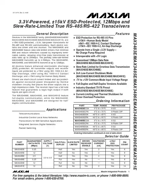
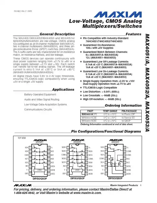
MAX4023EEE+T中文资料
- 格式:pdf
- 大小:474.42 KB
- 文档页数:22
General DescriptionThe MAX4023–MAX4026 family of voltage feedback multiplexer-amplifiers combine low-glitch switching and excellent video specifications with fixed or settable gain. The MAX4024/MAX4026 are triple and quad 2:1multiplexers, respectively, with amplifiers that have a fixed gain of +2. The MAX4023/MAX4025 are triple and quad 2:1 multiplexers, respectively, with adjustable gain amplifiers optimized for unity-gain stability. All devices have 25ns channel switching time and low 10mV P-P switching transients, making them ideal for high-speed video-switching applications. These devices operate from a single +4.5V to +11V supply or from dual supplies of ±2.25V to ±5.5V, and feature an input common-mode voltage range that extends to the negative supply rail. A low-power disable mode places the output in a high-impedance state.The MAX4023/MAX4025 have -3dB bandwidths of 260MH z and up to 330V/µs slew rates with a settable gain to equalize long cable runs. The MAX4024/MAX4026, with 200MHz -3dB bandwidths and 363V/µs slew rates, have a fixed gain of +2 for driving short back-terminated cables. The MAX4023/MAX4025 inter-nal amplifiers maintain an open-loop output impedance of only 18Ωover the full output voltage range, and mini-mize the gain error and bandwidth changes under loads typical of most Rail-to-Rail ®amplifiers. These devices are ideal for broadcast video applications with differential gain and phase errors of 0.07% and 0.07°,respectively.ApplicationsSet-Top BoxesIn-Car Navigation/Entertainment ServersSecurity Systems Video Projectors Notebook Computers Broadcast VideoVideo Crosspoint SwitchingFeatureso Single +5V or Dual ±5V Operationo 260MHz -3dB Bandwidth (MAX4023/MAX4025)o 200MHz -3dB Bandwidth (MAX4024/MAX4026)o 363V/µs Slew Rate (MAX4024/MAX4026)o 25ns Channel Switching Timeo Ultra-Low 20mV P-P Switching Transient o 0.012%/0.05°Differential Gain/Phase Error o Input Common-Mode Range Includes Negative Rail (MAX4023/MAX4025)o Low-Power Disable Modeo Available in Space-Saving 14-Pin TSSOP and 16-Pin QSOP PackagesMAX4023–MAX4026Triple and Quad, 2:1 Video Multiplexer-Amplifiers with Fixed and Settable Gain________________________________________________________________Maxim Integrated Products 1Typical Operating Circuit19-2758; Rev 0; 1/03For pricing, delivery, and ordering information,please contact Maxim/Dallas Direct!at 1-888-629-4642, or visit Maxim’s website at .Ordering InformationSelector Guide and Pin Configurations appear at end of data sheet.Rail-to-Rail is a registered trademark of Nippon Motorola, Ltd.M A X 4023–M A X 4026Triple and Quad, 2:1 Video Multiplexer-Amplifiers with Fixed and Settable Gain 2_______________________________________________________________________________________ABSOLUTE MAXIMUM RATINGSStresses beyond those listed under “Absolute Maximum Ratings” may cause permanent damage to the device. These are stress ratings only, and functional operation of the device at these or any other conditions beyond those indicated in the operational sections of the specifications is not implied. Exposure to absolute maximum rating conditions for extended periods may affect device reliability.Supply Voltage (V CC to V EE )..................................................12V IN_A, IN_B, FB_...............................(V EE - 0.3V) to (V CC + 0.3V)REF, EN, A/B....................................(V EE - 0.3V) to (V CC + 0.3V)Current Into IN_A, IN_B, FB_............................................±20mA Short-Circuit Duration (OUT_ to GND or V EE )............Continuous Short-Circuit Duration (OUT_ to V CC )..............................(Note 1)Continuous Power Dissipation (T A = +70°C)14-Pin TSSOP (derate 9.1mW/°C above +70°C).........727mW 14-Pin Narrow SO (derate 8.3mW/°C above +70°C)...667mW 16-Pin QSOP (derate 8.3mW/°C above +70°C)...........667mW 16-Pin Narrow SO (derate 8.7mW/°C above +70°C)...696mW 20-Pin TSSOP (derate 10.9mW/°C above +70°C).......879mW 20-Pin Wide SO (derate 10mW/°C above +70°C)........800mW Operating Temperature Range ...........................-40°C to +85°C Junction Temperature......................................................+150°C Storage Temperature Range.............................-65°C to +150°C Lead Temperature (soldering, 10s).................................+300°CNote 1:Do not short OUT_ to V CC .DC ELECTRICAL CHARACTERISTICS—Dual SupplyMAX4023–MAX4026Triple and Quad, 2:1 Video Multiplexer-Amplifiers with Fixed and Settable Gain_______________________________________________________________________________________3DC ELECTRICAL CHARACTERISTICS —Dual Supply (continued)M A X 4023–M A X 4026Triple and Quad, 2:1 Video Multiplexer-Amplifiers with Fixed and Settable Gain 4_______________________________________________________________________________________DC ELECTRICAL CHARACTERISTICS —Single Supply(V= +5V, V = 0V, R = ∞, EN = +5V, V = REF = OUT = 0.5V, T = T to T , unless otherwise noted. Typical values are atMAX4023–MAX4026Triple and Quad, 2:1 Video Multiplexer-Amplifiers with Fixed and Settable Gain_______________________________________________________________________________________5DC ELECTRICAL CHARACTERISTICS —Single Supply (continued)(V CC = +5V, V EE = 0V, R L = ∞, EN = +5V, V CM = REF = OUT = 0.5V, T A = T MIN to T MAX , unless otherwise noted. Typical values are at T A = +25°C.) (Note 2)M A X 4023–M A X 4026Triple and Quad, 2:1 Video Multiplexer-Amplifiers with Fixed and Settable Gain 6_______________________________________________________________________________________AC ELECTRICAL CHARACTERISTICS —Dual SupplyMAX4023–MAX4026Triple and Quad, 2:1 Video Multiplexer-Amplifiers with Fixed and Settable Gain_______________________________________________________________________________________7AC ELECTRICAL CHARACTERISTICS —Single SupplyM A X 4023–M A X 4026Triple and Quad, 2:1 Video Multiplexer-Amplifiers with Fixed and Settable Gain 8_______________________________________________________________________________________Typical Operating Characteristics—±5V Dual Supply(V CC = +5V, V EE = -5V, V CM = REF = 0V, EN = +5V, R IN = 75Ωto GND, R L = 150Ωto GND, A VCL = +1V/V (MAX4023/MAX4025),A VCL = +2V/V (MAX4024/MAX4026), T A = +25°C, unless otherwise noted.)MAX4023/MAX4025SMALL-SIGNAL BANDWIDTH vs. FREQUENCYM A X 4023/25 t o c 01FREQUENCY (MHz)G A I N (d B )100101-4-3-2-1012345-50.11000MAX4023/MAX4025SMALL-SIGNAL GAIN FLATNESS vs. FREQUENCYM A X 4023/25 t o c 02FREQUENCY (MHz)G A I N (d B )100101-0.4-0.3-0.2-0.100.10.20.30.40.5-0.50.11000MAX4023/MAX4025LARGE-SIGNAL BANDWIDTH vs. FREQUENCYM A X 4023/25 t o c 03FREQUENCY (MHz)G A I N (d B )100101-4-3-2-1012345-50.11000MAX4023/MAX4025LARGE-SIGNAL GAIN FLATNESSvs. FREQUENCYM A X 4023/25 t o c 04FREQUENCY (MHz)G A I N (d B )100101-0.4-0.3-0.2-0.100.10.20.30.40.5-0.50.11000MAX4024/MAX4026SMALL-SIGNAL BANDWIDTH vs. FREQUENCYM A X 4023/25 t o c 05FREQUENCY (MHz)N O R M A L I Z E D G A I N (d B )100101-4-3-2-1012345-50.11000MAX4024/MAX4026SMALL-SIGNAL GAIN FLATNESSvs. FREQUENCYM A X 4023/25 t o c 06FREQUENCY (MHz)N O R M A L I Z E D G A I N (d B )100101-0.4-0.3-0.2-0.100.10.20.30.40.5-0.50.11000MAX4024/MAX4026LARGE-SIGNAL BANDWIDTH vs. FREQUENCYM A X 4023/25 t o c 07FREQUENCY (MHz)N O R M A L I Z E D G A I N (d B )100101-4-3-2-1012345-50.11000MAX4024/MAX4026LARGE-SIGNAL GAIN FLATNESSvs. FREQUENCYM A X 4023/25 t o c 08FREQUENCY (MHz)N O R M A L I Z E D G A I N (d B )100101-0.4-0.3-0.2-0.100.10.20.30.40.5-0.50.110006th5th4th3rd2nd1stMAX4023/MAX4025DIFFERENTIAL GAIN AND PHASED I F FE R E N T I A L P H A S E (°)D I F FE R E N T I A L G A I N (%)MAX4023–MAX4026Triple and Quad, 2:1 Video Multiplexer-Amplifiers with Fixed and Settable Gain_______________________________________________________________________________________96th5th4th3rd2nd1stMAX4024/MAX4026DIFFERENTIAL GAIN AND PHASED I F FE R E N T I A L P H A S E (°)D I F FE R EN T I A L G A I N (%)POWER-SUPPLY REJECTION RATIOvs. FREQUENCYFREQUENCY (MHz)P S R R (d B )1010.1-100-80-60-40-200-1200.01100-1000.010.11001000MAX4023/MAX4025COMMON-MODE REJECTION RATIOvs. FREQUENCY-80-60-40-20FREQUENCY (MHz)C M R R (d B )1101101001000OFF-ISOLATION vs. FREQUENCYFREQUENCY (MHz)O F F -I S O L A T I O N (d B )0-120-100-80-60-40-20FREQUENCY (MHz)C R O S S T A L K (d B )1001011000ALL-HOSTILE CROSSTALKvs. FREQUENCYM A X 4023/25 t o c 14-80-60-40-200-1001000.111001000OUTPUT IMPEDANCE vs. FREQUENCY110FREQUENCY (MHz)O U T P U T I M P E D A N C E (Ω)101000100.010.11001000INPUT VOLTAGE-NOISE DENSITYvs. FREQUENCY100FREQUENCY (kHz)110V O L T A G E -N O I S E D E N S I T Y (n V /H z )MAX4023/MAX4025LARGE-SIGNAL TRANSIENT RESPONSEM A X 4023/25 t o c 1720ns/divINPUT 1V/div OUTPUT 1V/divMAX4023/MAX4025SMALL-SIGNAL TRANSIENT RESPONSEM A X 4023/25 t o c 1820ns/divINPUT 50mV/divOUTPUT 50mV/divTypical Operating Characteristics—±5V Dual Supply (continued)(V CC = +5V, V EE = -5V, V CM = REF = 0V, EN = +5V, R IN = 75Ωto GND, R L = 150Ωto GND, A VCL = +1V/V (MAX4023/MAX4025),A VCL = +2V/V (MAX4024/MAX4026), T A = +25°C, unless otherwise noted.)M A X 4023–M A X 4026Triple and Quad, 2:1 Video Multiplexer-Amplifiers with Fixed and Settable Gain 10______________________________________________________________________________________MAX4024/MAX4026LARGE-SIGNAL TRANSIENT RESPONSEM A X 4023/25 t o c 1920ns/div INPUT 500mV/div OUTPUT 1V/div MAX4024/MAX4026SMALL-SIGNAL TRANSIENT RESPONSEM A X 4023/25 t o c 2020ns/div INPUT 25mV/divOUTPUT 50mV/div CHANNEL SWITCHING TRANSIENTMA X 4023/25 t o c 2120ns/divV A/B 5V/divV OUT 20mV/divENABLE RESPONSE TIMEM A X 4023/25 t o c 2220ns/divV EN 5V/divV OUT 500mV/divMAX4023/MAX4025SMALL-SIGNAL BANDWIDTH vs. FREQUENCY vs. C LFREQUENCY (MHz)G A I N (d B )100101.0-4-3-2-1012345-51000OPTIMAL ISOLATION RESISTORvs. CAPACITIVE LOADCAPACITIVE LOAD (pF)O P T I M A L I S O L A T I O N R E S I S T O R (Ω)1502001005010203040500250Typical Operating Characteristics—±5V Dual Supply (continued)(V CC = +5V, V EE = -5V, V CM = REF = 0V, EN = +5V, R IN = 75Ωto GND, R L = 150Ωto GND, A VCL = +1V/V (MAX4023/MAX4025),A VCL = +2V/V (MAX4024/MAX4026), T A = +25°C, unless otherwise noted.)MAX4023–MAX4026Triple and Quad, 2:1 Video Multiplexer-Amplifiers with Fixed and Settable GainMAX4023/MAX4025SMALL-SIGNAL BANDWIDTH vs. FREQUENCYM A X 4023/25 t o c 25FREQUENCY (MHz)N O R M A L I Z E D G A I N (d B )100101-4-3-2-1012345-50.11000MAX4023/MAX4025SMALL-SIGNAL GAIN FLATNESSvs. FREQUENCYM A X 4023/25 t o c 26FREQUENCY (MHz)G A I N (d B )100101-0.4-0.3-0.2-0.100.10.20.30.40.5-0.50.11000MAX4023/MAX4025LARGE-SIGNAL BANDWIDTHvs. FREQUENCYM A X 4023/25 t o c 27FREQUENCY (MHz)G A I N (d B )100101-4-3-2-1012345-50.11000MAX4023/MAX4025LARGE-SIGNAL GAIN FLATNESSvs. FREQUENCYM A X 4023/25 t o c 28FREQUENCY (MHz)G A I N (d B )100101-0.4-0.3-0.2-0.100.10.20.30.40.5-0.50.11000MAX4024/MAX4026SMALL-SIGNAL BANDWIDTH vs. FREQUENCYM A X 4023/25 t o c 29FREQUENCY (MHz)N O R M A L I Z E D G A I N (d B )100101-4-3-2-1012345-50.11000MAX4024/MAX4026SMALL-SIGNAL GAIN FLATNESSvs. FREQUENCYM A X 4023/25 t o c 30FREQUENCY (MHz)N O R M A L I Z E D G A I N (d B )100101-0.5-0.6-0.4-0.30.10-0.1-0.20.20.30.40.50.60.7-0.70.11000MAX4024/MAX4026LARGE-SIGNAL BANDWIDTH vs. FREQUENCYM A X 4023/25 t o c 31FREQUENCY (MHz)N O R M A L I Z E D G A I N (d B )100101-4-3-2-1012345-50.11000MAX4024/MAX4026LARGE-SIGNAL GAIN FLATNESSvs. FREQUENCYM A X 4023/25 t o c 32FREQUENCY (MHz)N O R M A L I Z E D G A I N (d B )100101-0.4-0.3-0.2-0.100.10.20.30.40.50.50.11000Typical Operating Characteristics—+5V Single Supply(V CC = +5V, V EE = 0V, V CM = 0.5V, V REF = V CM , EN = +5V, R IN = 75Ωto V CM , R L = 150Ωto GND, A VCL = +1V/V (MAX4023/MAX4025), A VCL = +2V/V (MAX4024/MAX4026), T A = +25°C, unless otherwise noted.)M A X 4023–M A X 4026Triple and Quad, 2:1 Video Multiplexer-Amplifiers with Fixed and Settable Gain Typical Operating Characteristics—+5V Single Supply (continued)(V CC = +5V, V EE = 0V, V CM = 0.5V, V REF = V CM , EN = +5V, R IN = 75Ωto V CM , R L = 150Ωto GND, A VCL = +1V/V (MAX4023/MAX4025), A VCL = +2V/V (MAX4024/MAX4026), T A = +25°C, unless otherwise noted.)6th5th4th3rd2nd1st 6th5th4th3rd2nd1stMAX4023/MAX4025DIFFERENTIAL GAIN AND PHASE-0.2-0.3-0.100.10.20.3-0.2-0.3-0.100.10.20.3D I F F E R E N T I A L P H A S E (°)D I F FE R E N T I A L G A I N (%)M A X 4023/25 t o c 336th5th4th3rd2nd1st6th5th4th3rd2nd1stMAX4024/MAX4026DIFFERENTIAL GAIN AND PHASE-0.2-0.3-0.100.10.20.3-0.2-0.3-0.100.10.20.3D I F F E R E N T I A L P H A S E (°)D I F FE R E N T I A L G A I N (%)M A X 4023/25 t o c 34MAX4023–MAX4026Triple and Quad, 2:1 Video Multiplexer-Amplifiers with Fixed and Settable GainM A X 4023–M A X 4026Triple and Quad, 2:1 Video Multiplexer-Amplifiers with Fixed and Settable Gain Detailed DescriptionThe MAX4024/MAX4026 combine three and four 2:1multiplexers, respectively, with a fixed gain of 2 amplifi-er. The MAX4023/MAX4025 combine three and four 2:1multiplexers, respectively, with an adjustable gain out-put amplifier optimized for a closed-loop gain of +1 or greater. These devices operate from a single-supply voltage of +4.5V to +11V or from dual supplies of ±2.25V to ±5.5V. The outputs may be placed in a high-impedance state and the supply current minimized by forcing the EN pin low. The input multiplexers feature short 25ns channel-switching times and small 10mV P-P switching transients. These devices feature voltage-feedback output amplifiers that achieve up to 363V/µs slew rates and up to 220MH z -3dB bandwidths. They also feature excellent differential gain/phase perfor-mance.The MAX4023–MAX4026 feature an A/B pin, which is an input pin for selecting either channel A or B. Drive A/B high to select channel A or drive A/B low to select channel B. Channel A is automatically selected if A/B is left unconnected.Applications InformationFeedback and Gain Resistor Selection(MAX4023/MAX4025)Select the MAX4023/MAX4025 gain-setting feedback R F and R G resistors to fit your application. Large resis-tor values increase voltage noise and interact with the amplifier ’s input and PC board capacitance. This can generate undesirable poles and zeros, and can decrease bandwidth or cause oscillations.Stray capacitance at the FB pin produces peaking in the frequency-response curve. Keep the capacitance at FB as low as possible by using surface-mount resis-tors and by avoiding the use of a ground plane beneath or beside these resistors and the FB pin. Some capaci-tance is unavoidable. If necessary, its effects can be neutralized by adjusting R F . Use 1% resistors to main-tain gain accuracy.Low-Power Shutdown ModeAll parts feature a low-power shutdown mode that is activated by driving the EN input low. Placing the amplifier in shutdown mode reduces the quiescent sup-ply current to below 4mA and places the output into a high-impedance state, typically 75k Ω(MAX4023/MAX4025). Multiple devices may be paralleled to con-struct larger switch matrices by connecting the outputs of several devices together and disabling all but one of the paralleled amplifiers ’ outputs.For MAX4023/MAX4025 application circuits operating with a closed-loop gain of +1 or greater, consider the external-feedback network impedance of all devices used in the mux application when calculating the total load on the output amplifier of the active device. The MAX4024/MAX4026 have a fixed gain of +2 that is internally set with two 500Ωthin-film resistors. The impedance of the internal feedback resistors must be taken into account when operating multiple MAX4024/MAX4026s in large multiplexer applications.For normal operation, drive EN high. Note that the MAX4023–MAX4026 have internal pullup circuitry on EN, so if left unconnected, it is automatically pulled up to V CC .Layout and Power-Supply BypassingThe MAX4023–MAX4026 have high bandwidths and consequently require careful board layout, including the possible use of constant-impedance microstrip or stripline techniques.To realize the full AC performance of these high-speed amplifiers, pay careful attention to power-supply bypassing and board layout. The PC board should have at least two layers: a signal and power layer on one side, and a large, low-impedance ground plane on the other side. The ground plane should be as free of voids as possible, with one exception: The feedback (FB) should have as low a capacitance to ground as possible. Whether or not a constant-impedance board is used, it is best to observe the following guidelines when designing the board:1)Do not use wire-wrapped boards or breadboards.2)Do not use IC sockets; they increase parasiticcapacitance and inductance.3)Keep signal lines as short and straight as possible.Do not make 90°turns; round all corners.4)Observe high-frequency bypassing techniques tomaintain the amplifier ’s accuracy and stability.5)Use surface-mount components. They generallyhave shorter bodies and lower parasitic reactance,yielding better high-frequency performance than through-hole components.The bypass capacitors should include a 0.1µF ceramic surface-mount capacitor between each supply pin and the ground plane, located as close to the package as possible. Optionally, place a 10µF tantalum capacitor at the power-supply ’s point of entry to the PC board to ensure the integrity of incoming supplies. The power-supply traces should lead directly from the tantalum capacitor to the V CC and V EE pins. To minimize para-sitic inductance, keep PC traces short and use surface-mount components.If input termination resistors and output back-termina-tion resistors are used, they should be surface-mount types, and should be placed as close to the IC pins as possible.Video Line Driver The MAX4024/MAX4026 are well suited to drive short coaxial transmission lines when the cable is terminated at both ends (as shown in Figure 2a) where the fixed gain of +2 compensates for the loss in the resistors. The MAX4023/MAX4025 have settable gain to equalize long cables. The MAX4023/MAX4025 allow adding functions that normally require additional op amps. For example, a cable driver can “boost” the high frequen-cies for long runs, making the part perform multiple functions. Figure 2b shows the “cable booster” using the MAX4023/MAX4025.Driving Capacitive Loads A correctly terminated transmission line is purely resis-tive and presents no capacitive load to the amplifier.Reactive loads decrease phase margin and may pro-duce excessive ringing and oscillation (see Typical Operating Characteristics).Another concern when driving capacitive loads is the amplifier’s output impedance, which appears inductiveat high frequencies. This inductance forms an L-C reso-nant circuit with the capacitive load, which causes peaking in the frequency response and degrades the amplifier’s phase margin.Although the MAX4023–MAX4026 are optimized for AC performance and are not designed to drive highly capacitive loads, they are capable of driving up to33pF without oscillations. However, some peaking mayoccur in the frequency domain (Figure 3). To drive larg-er capacitive loads or to reduce ringing, add an isola-tion resistor between the amplifier’s output and the load (Figure 4). The value of R ISO depends on the circuit’sgain and the capacitive load (Figure 5). Also note thatthe isolation resistor forms a divider that decreases the voltage delivered to the load.MAX4023–MAX4026Triple and Quad, 2:1 Video Multiplexer-Amplifiers with Fixed and Settable Gain Figure 1. MAX4023/MAX4025 Noninverting Gain ConfigurationM A X 4023–M A X 4026Triple and Quad, 2:1 Video Multiplexer-Amplifiers with Fixed and Settable Gain Figure 2b. Cable Booster Using the MAX4023/MAX4025Figure 2a. Video Line DriverMAX4023–MAX4026Triple and Quad, 2:1 Video Multiplexer-Amplifiers with Fixed and Settable GainSelector GuideChip InformationTRANSISTOR COUNT: 655PROCESS: BipolarFigure 3. Small-Signal Bandwidth vs. Frequency with Capacitive Load and No Isolation ResistorFigure 4. Using an Isolation Resistor (R ISO ) for a High-Capacitive LoadFigure 5. Optimal Isolation Resistance vs. Capacitive LoadM A X 4023–M A X 4026Triple and Quad, 2:1 Video Multiplexer-Amplifiers with Fixed and Settable GainPin ConfigurationsMAX4023–MAX4026Triple and Quad, 2:1 Video Multiplexer-Amplifiers with Fixed and Settable GainPackage Information(The package drawing(s) in this data sheet may not reflect the most current specifications. For the latest package outline information,go to /packages .)M A X 4023–M A X 4026Triple and Quad, 2:1 Video Multiplexer-Amplifiers with Fixed and Settable Gain Package Information (continued)(The package drawing(s) in this data sheet may not reflect the most current specifications. For the latest package outline information,go to /packages .)MAX4023–MAX4026Triple and Quad, 2:1 Video Multiplexer-Amplifiers with Fixed and Settable Gain______________________________________________________________________________________21Package Information (continued)(The package drawing(s) in this data sheet may not reflect the most current specifications. For the latest package outline information,go to /packages .)Package Information (continued)(The package drawing(s) in this data sheet may not reflect the most current specifications. For the latest package outline information,go to /packages .)M A X 4023–M A X 4026Triple and Quad, 2:1 Video Multiplexer-Amplifiers with Fixed and Settable Gain Maxim cannot assume responsibility for use of any circuitry other than circuitry entirely embodied in a Maxim product. No circuit patent licenses are implied. Maxim reserves the right to change the circuitry and specifications without notice at any time.22____________________Maxim Integrated Products, 120 San Gabriel Drive, Sunnyvale, CA 94086 408-737-7600©2003 Maxim Integrated ProductsPrinted USAis a registered trademark of Maxim Integrated Products.。