
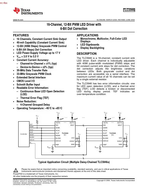
TLC5946RHBR;TLC5946PW;TLC5946PWP;TLC5946PWPR;TLC5946PWR;中文规格书,Datasheet资料
- 格式:pdf
- 大小:1.10 MB
- 文档页数:11
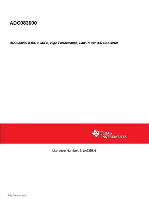
ADC083000ADC083000 8-Bit, 3 GSPS, High Performance, Low Power A/D ConverterLiterature Number: SNAS358NADC0830008-Bit, 3 GSPS, High Performance, Low Power A/D ConverterGeneral DescriptionThe ADC083000 is a single, low power, high performance CMOS analog-to-digital converter that digitizes signals to 8 bits resolution at sampling rates up to 3.4 GSPS. Consuming a typical 1.9 Watts at 3 GSPS from a single 1.9 Volt supply, this device is guaranteed to have no missing codes over the full operating temperature range. The unique folding and in-terpolating architecture, the fully differential comparator de-sign, the innovative design of the internal sample-and-hold amplifier and the self-calibration scheme enable an excellent response of all dynamic parameters up to Nyquist, producing a high 7.0 Effective Number Of Bits, (ENOB) with a 748 MHz input signal and a 3 GHz sample rate while providing a 10-18 Word Error Rate. The ADC083000 achieves a 3 GSPS sam-pling rate by utilizing both the rising and falling edge of a 1.5 GHz input clock. Output formatting is offset binary and the LVDS digital outputs are compatible with IEEE 1596.3-1996, with the exception of an adjustable common mode voltage between 0.8V and 1.15V.The ADC has a 1:4 demultiplexer that feeds four LVDS buses and reduces the output data rate on each bus to a quarter of the sampling rate.The converter typically consumes less than 25 mW in the Power Down Mode and is available in a 128-lead, thermally enhanced exposed pad LQFP and operates over the Indus-trial (-40°C ≤ T A≤ +85°C) temperature range.Features■Single +1.9V ±0.1V Operation■Choice of SDR or DDR output clocking■Serial Interface for Extended Control■Adjustment of Input Full-Scale Range and Offset■Duty Cycle Corrected Sample Clock■Test patternKey Specifications■Resolution8 Bits ■Max Conversion Rate 3 GSPS (min)■Error Rate10-18 (typ)■ENOB @ 748 MHz Input7.0 Bits (typ)■SNR @ 748 MHz44.5 dB (typ)■Full Power Bandwidth 3 GHz (typ)■Power Consumption—Operating 1.9 W (typ)—Power Down Mode25 mW (typ) Applications■Direct RF Down Conversion■Digital Oscilloscopes■Satellite Set-top boxes■Communications Systems■Test InstrumentationOrdering InformationIndustrial Temperature Range(-40°C < TA < +85°C)NS PackageADC083000CIYB128-Pin Exposed Pad LQFPADC083000RB Reference Board© 2009 National Semiconductor C083000 8-Bit, 3 GSPS, High Performance, Low Power A/D ConverterBlock Diagram20 2A D C 020193201Note: The exposed pad on the bottom of the package must be soldered to a ground plane to ensure rated performance. 083000Pin Functions Pin No.SymbolEquivalent CircuitDescription3OutV / SCLKOutput Voltage Amplitude / Serial Interface Clock(Input):LVCMOS Tie this pin high for normal differential DC and data amplitude. Ground this pin for a reduced differentia output amplitude and reduced power consumption. See Sect 1.1.6. When the extended control mode is enabled, this pin functions as the SCLK input which clocks in the serial data. S Section 1.2 for details on the extended control mode. See Section 1.3 for description of the serial interface.4OutEdge / DDR /SDATAEdge Select / Double Data Rate / Serial Data(Input):LVCMOS This input sets the output edge of DCLK+which the output data transitions. (See Section 1.1.5.2). Whe this pin is floating or connected to 1/2 the supply voltage, DD clocking is enabled. When the extended control mode is enabl this pin functions as the SDATA input. See Section 1.2 for det on the extended control mode. See Section 1.3 for description the serial interface.15DCLK_RSTDCLK Reset(Input):LVCMOS A positive pulse on this pin is used to rese and synchronize the DCLK outs of multiple converters. See Section 1.5 for detailed description. When bit 14 in theConfiguration Register (address 1h) is set to 0b, this single-ended DCLK_RST pin is selected. See also pins 22,23description.26PDPower Down(Input):LVCMOS A logic high on the PD pin puts the entire device into the Power Down Mode.30CALCalibration Cycle Initiate(Input):LVCMOS A minimum 80 input clock cycles logic low followed by a minimum of 80 input clock cycles high on this p initiates the calibration sequence. See Section 2.4.2 for an overview of self-calibration and Section 2.4.2.2 for a descript of on-command calibration.14FSR/ECEFull Scale Range Select / Extended Control Enable(Input):LVCMOS In non-extended control mode, a logic low this pin sets the full-scale differential input range to 600 mV P A logic high on this pin sets the full-scale differential input ran to 820 mV P-P . See Section 1.1.4. To enable the extended con mode, whereby the serial interface and control registers are employed, allow this pin to float or connect it to a voltage equ to V A /2. See Section 1.2 for information on the extended con mode. 4A D C 0Pin No.Symbol Equivalent Circuit Description127CalDly / SCSCalibration Delay / Serial Interface Chip Select(Input):LVCMOS With a logic high or low on pin 14, this pin functions as Calibration Delay and sets the number of input clock cycles after power up before calibration begins (See Section 1.1.1). With pin 14 floating, this pin acts as the enable pin for the serial interface input and the CalDly value becomes "0" (short delay with no provision for a long power-up calibration delay).1011CLK+CLK-Sampling Clock Input(Input):LVDS The differential clock signal must be a.c. coupled to these pins. The input signal is sampled on both the rising and falling edge of CLK. See Section 1.1.2 for a description ofacquiring the input and Section 2.3 for an overview of the clock inputs.1819V IN +V IN −Signal Input(Input):Analog The differential full-scale input range is 600mV P-P when the FSR pin is low, or 820 mV P-P when the FSR pin is high. In the Extended Control Mode, FSR is determined by the Full-Scale Voltage Adjust register (address 3h, bits 15:7).2223DCLK_RST+DCLK_RST-Sample Clock Reset(Input):LVDS A positive differerntial pulse on these pins is used to reset and synchronize the DCLK outs of multiple converters.See Section 1.5 for detailed description. When bit 14 in theConfiguration Register (address 1h) is set to 1b, these differential DCLK_RST pins are selected. See also pin 15 description.7V CMOCommon Mode Voltage(Output):Analog - The voltage output at this pin is required to be the common mode input voltage at V IN + and V IN − when d.c.coupling is used. This pin should be grounded when a.c. coupling is used at the analog input. This pin is capable of sourcing or sinking 100μA and can drive a load up to 80 pF. See Section 2.2.083000Pin No.Symbol Equivalent CircuitDescription31V BGBandgap Output Voltage(Output):Analog - Capable of 100 μA source/sink and can dr a load up to 80 pF.126CalRunCalibration Running(Output):LVCMOS - This pin is at a logic high while a calibrat is running.32R EXTExternal Bias Resistor ConnectionAnalog - Nominal value is 3.3k-Ohms (±0.1%) to ground. S Section 1.1.1.3435Tdiode_P Tdiode_NTemperature DiodeAnalog - Positive (Anode) and Negative (Cathode). These p may be used for die temperature measurements, however no specified accuracy is implied or guaranteed. Noise coupling fr adjacent output data signals has been shown to affecttemperature measurements using this feature. See Section 2.6.2. 6A D C 0Pin No.Symbol Equivalent Circuit Description36 / 37 38 / 39 43 / 44 45 / 46 47 / 48 49 / 50 54 / 55 56 / 57 58 / 59 60 / 61 65 / 66 67 / 68 69 / 70 71 / 72 75 / 76 77 / 78Da0+ / Da0-Da1+ / Da1-Da2+ / Da2−Da3+ / Da3-Da4+ / Da4−Da5+ / Da5-Da6+ / Da6−Da7+ / Da7-Dc0+ / Dc0-Dc1+ / Dc1-Dc2+ / Dc2−Dc3+ / Dc3-Dc4+ / Dc4−Dc5+ / Dc5-Dc6+ / Dc6−Dc7+ / Dc7-A and C Data(Output):LVDS Data Outputs from the first internal converter.The data should be extracted in the order ABCD. These outputsshould always be terminated with a 100Ω differential resistor atthe receiver.83 / 84 85 / 86 89 / 90 91 / 92 93 / 94 95 / 96 100 / 101 102 / 103 104 / 105 106 / 107 111 / 112 113 / 114 115 / 116 117 / 118 122 / 123 124 / 125Dd7− / Dd7+Dd6- / Dd6+Dd5− / Dd5+Dd4- / Dd4+Dd3- / Dd3+Dd2- / Dd2+Dd1− / Dd1+Dd0- / Dd0+Db7- / Db7+Db6- / Db6+Db5− / Db5+Db4- / Db4+Db3− / Db3+Db2- / Db2+Db1− / Db1+Db0- / Db0+B and D Data(Output):LVDS Data Outputs from the second internalconverter. The data should be extracted in the order ABCD.These outputs should always be terminated with a 100Ωdifferential resistor at the receiver.79 80OR+OR-Out Of Range(Output):LVDS - A differential high at these pins indicates thatthe differential input is out of range (outside the range ±325 mVor ±435 mV as defined by the FSR pin). These outputs shouldalways be terminated with a 100Ω differential resistor at thereceiver.82 81DCLK+DCLK-Differential Clock(Output):LVDS - The Differential Clock output used to latch theoutput data. Delayed and non-delayed data outputs are suppliedsynchronous to this signal. DCLK is 1/2 the sample clock rate inSDR mode and 1/4 the sample clock rate in the DDR mode.These outputs should always be terminated with a 100Ωdifferential resistor at the receiver. The DCLK outputs may notbe active during the calibration cycle depending upon the settingof Configuration Register (address 1h), bit- 14 (RTD). SeeSection 1.1.1.083000Pin No.Symbol Equivalent Circuit Description2, 5, 8, 13,16, 17, 20,25, 28, 33,128V AAnalog power supply pins(Power) - Bypass these pins to ground.40, 51 ,62,73, 88, 99,110, 121V DROutput Driver power supply pins(Power) - Bypass these pins to DR GND.1, 6, 9, 12,21, 24, 27GND(Gnd) - Ground return for V A .42, 53, 64,74, 87, 97,108, 119DR GND(Gnd) - Ground return for V DR .29,41,52,63, 98, 109,120NC No Connection Make no connection to these pins 8A D C 0(Notes 1, 2)If Military/Aerospace specified devices are required,please contact the National Semiconductor Sales Office/Distributors for availability and specifications.Supply Voltage (V A , V DR ) 2.2VSupply Difference V A - V DR0V to -100mVVoltage on Any Input Pin (Except V IN +, V IN -)−0.15V to (V A + 0.15V)Voltage on V IN +, V IN -(Maintaining Common Mode)-0.15V to 2.5V Ground Difference |GND - DR GND|0V to 100 mVInput Current at Any Pin (Note 3)±25 mA Package Input Current (Note 3)±50 mAPower Dissipation at T A ≤ 85°C 2.3 WESD Susceptibility (Note 4) Human Body Model Machine Model 2500V 250VStorage Temperature−65°C to +150°CSolder i ng process must comply w i th Nat i onal Semiconductor’s Reflow Temperature Profile specifications.Refer to /packaging. (Note 5)Ambient Temperature Range −40°C ≤ T A ≤ +85°C Supply Voltage (V A )+1.8V to +2.0V Driver Supply Voltage (V DR )+1.8V to V A Analog Input Common Mode Voltage V CMO ±50mV V IN +, V IN - Voltage Range (Maintaining Common Mode)0V to 2.15V (100% duty cycle)0V to 2.5V (10% duty cycle)Ground Difference(|GND - DR GND|)0V CLK Pins Voltage Range 0V to V ADifferential CLK Amplitude0.4V P-P to 2.0V P-PPackage Thermal ResistancePackage θJA θJC (Top ofPackage)θJ-PAD(Thermal Pad)128-Lead Exposed PadLQFP26°C / W10°C / W 2.8°C / WConverter Electrical CharacteristicsThe following specifications apply after calibration for V A = V DR = +1.9V DC , OutV = 1.9V, V IN FSR (a.c. coupled) = differential 820mV P-P , C L = 10 pF, Differential a.c. coupled Sinewave Input Clock, f CLK = 1.5GHz at 0.5V P-P with 50% duty cycle, V BG = Floating,Non-Extended Control Mode, SDR Mode, R EXT = 3300Ω ±0.1%, Analog Signal Source Impedance = 100Ω Differential, after cali-bration. Boldface limits apply for T A = T MIN to T MAX . All other limits T A = 25°C, unless otherwise noted. (Notes 6, 7)SymbolParameterConditionsTypical (Note 8)Limits (Note 8)Units (Limits)STATIC CONVERTER CHARACTERISTICS INL Integral Non-Linearity (Best fit)DC Coupled, 1MHz Sine Wave Over Ranged±0.35±0.9LSB (max)DNL Differential Non-Linearity DC Coupled, 1MHz Sine Wave Over Ranged ±0.20±0.6LSB (max)Resolution with No Missing Codes 8Bits V OFF Offset Error-0.20 LSB V OFF _ADJ Input Offset Adjustment Range Extended Control Mode±45 mV PFSE Positive Full-Scale Error (Note 9)−1.6±25mV (max)NFSE Negative Full-Scale Error (Note 9)−1.00±25mV (max)FS_ADJ Full-Scale Adjustment Range Extended Control Mode ±20±15%FS DYNAMIC CONVERTER CHARACTERISTICSFPBW Full Power Bandwidth 3 GHz Word Error Rate10-18 Errors/SampleGain Flatness0.0 to -1.0 dBFS50 to 950 MHz ENOBEffective Number of Bitsf IN = 373 MHz, V IN = FSR − 0.5 dB 7.2 6.8Bits (min)f IN = 748 MHz, V IN = FSR − 0.5 dB 7.0 6.6Bits (min)f IN = 1498 MHz, V IN = FSR − 0.5 dB6.5Bits083000分销商库存信息: NATIONAL-SEMICONDUCTOR ADC083000CIYB/NOPB。

Data SheetADRF50541 GHz to 60 GHz, Reflective, Silicon SP4T Switch FEATURES►Ultrawideband frequency range: 1 GHz to 60 GHz►Low insertion loss►2.2 dB typical up to 40 GHz►2.8 dB typical up to 55 GHz►3.2 dB typical up to 60 GHz►High isolation►33 dB typical up to 40 GHz►28 dB typical up to 55 GHz►28 dB typical up to 60 GHz►High input linearity►P0.1dB: 25 dBm typical►IP3: 47 dBm typical►High RF power handling►Through path: 24 dBm►Hot switching path: 24 dBm►CMOS-/LVTTL-compatible►No low frequency spur►Fast RF switching time: 25 ns►RF settling time (50% V CTRL to 0.1 dB of RF OUT): 35 ns►Single-supply operation capability (VDD = 3.3 V, VSS = 0 V)►24-terminal, 3 mm × 3 mm, RoHS-compliant, LGA package APPLICATIONS►Industrial scanners►Test instrumentation►Cellular infrastructure—mmWave 5G►Military radios, radars, and electronic counter measures (ECMs)►Microwave radios and very small aperture terminals (VSATs)FUNCTIONAL BLOCK DIAGRAMFigure 1. Functional Block Diagram GENERAL DESCRIPTIONThe ADRF5054 is a reflective, SP4T switch manufactured in a silicon process. The ADRF5054 operates from 1 GHz to 60 GHz. The switch has a low insertion loss of 2.2 dB and 3.2 dB with33 dB and 28 dB isolation at 40 GHz and 60 GHz, respectively. The ADRF5054 has an RF input power handling capability of 24 dBm for the through and hot switching paths. The ADRF5054 requires dual-supply voltages of ±3.3 V. The ADRF5054 employs complementary metal-oxide semiconductor (CMOS)- and low volt-age transistor logic (LVTTL)-compatible control.The ADRF5054 can also operate with a single positive supply volt-age (V DD) applied while the negative supply voltage (V SS) is tied to ground. In this operating condition, the small signal performance is maintained while the switching characteristics, linearity, and power handling performance are derated (see Table 2 for more details). The ADRF5054 comes in a 24-terminal, 3 mm × 3 mm, RoHS compliant, land grid array (LGA) package and can operate from −40°C to +105°C.TABLE OF CONTENTSFeatures (1)Applications (1)Functional Block Diagram (1)General Description (1)Specifications (3)Single-Supply Operation (4)Absolute Maximum Ratings (5)Thermal Resistance (5)Power Derating Curve (5)Electrostatic Discharge (ESD) Ratings (5)ESD Caution (5)Pin Configuration and Function Descriptions (6)Interface Schematics (6)Typical Performance Characteristics (7)Insertion Loss, Return Loss, and Isolation (7)Input Power Compression and Third-OrderIntercept (9)Theory of Operation (10)RF Input and Output (10)Power Supply (10)Applications Information (11)Recommendations for PCB Design (11)Outline Dimensions (13)Ordering Guide (13)REVISION HISTORY5/2023—Revision 0: Initial VersionV DD = 3.3 V, V SS = −3.3 V, V1 = 0 V or V DD, V2 = 0 V or V DD, T CASE = 25°C for a 50 Ω system, unless otherwise noted. RFx refers to RF1 to RF4, and V CTRL is voltages of the digital inputs, V1 and V2.Table 1. Electrical CharacteristicsParameter Symbol Test Conditions/Comments Min Typ Max Unit FREQUENCY RANGE f160GHz INSERTION LOSSBetween RFC and RFx (On) 1 GHz to 18 GHz 1.7dB18 GHz to 40 GHz 2.2dB40 GHz to 55 GHz 2.8dB55 GHz to 60 GHz 3.2dB RETURN LOSSRFC 1 GHz to 18 GHz19dB18 GHz to 40 GHz20dB40 GHz to 55 GHz22dB55 GHz to 60 GHz18dB RF1 to RF4 (On) 1 GHz to 18 GHz23dB18 GHz to 40 GHz15dB40 GHz to 55 GHz22dB55 GHz to 60 GHz20dB ISOLATIONBetween RFC and RF1 (Off) or RFC and RF4 (Off) 1 GHz to 18 GHz42dB18 GHz to 40 GHz37dB40 GHz to 55 GHz28dB55 GHz to 60 GHz28dB Between RFC and RF2 (Off) or RFC and RF3 (Off) 1 GHz to 18 GHz41dB18 GHz to 40 GHz33dB40 GHz to 55 GHz31dB55 GHz to 60 GHz32dB Between RF1 and RF4 (Selected) and RF2 and RF3 (Off) 1 GHz to 18 GHz43dB18 GHz to 40 GHz36dB40 GHz to 55 GHz33dB55 GHz to 60 GHz36dB Between RF2 and RF3 (Selected) and RF1 and RF4 (Off) 1 GHz to 18 GHz45dB18 GHz to 40 GHz36dB40 GHz to 55 GHz37dB55 GHz to 60 GHz33dB SWITCHING CHARACTERISTICSRise Time and Fall Time t RISE, t FALL10% to 90% of RF output (RF OUT)5ns On Time and Off Time t ON, t OFF50% V CTRL to 90% of RF OUT25ns RF Settling Time0.1 dB50% V CTRL to 0.1 dB of final RF OUT35ns INPUT LINEARITY1 1 GHz to 60 GHz0.1 dB Power Compression P0.1dB25dBm Third-Order Intercept IP3Two-tone input power = 12 dBm each47dBmtone, Δf = 1 MHzSUPPLY CURRENT VDD and VSS pinsPositive Supply Current I DD145µA Negative Supply Current I SS510µATable 1. Electrical Characteristics (Continued)Parameter Symbol Test Conditions/Comments Min Typ Max Unit DIGITAL CONTROL INPUTS V1 and V2 pinsVoltageLow V INL00.8V High V INH 1.2 3.3V CurrentLow and High I INL, I INH<1µA RECOMMENDED OPERATING CONDITONSSupply VoltagePositive V DD 3.15 3.45V Negative V SS−3.45−3.15V Digital Control Voltage V CTRL0V DD V RF Input Power2, 3P IN f = 3 GHz to 60 GHz, T CASE = 85°C24dBm Through Path RF signal is applied to RFC or throughconnected RFx24dBm Hot Switching RF signal is present at RFC whileswitching between RFxCase Temperature T CASE−40+105°C 1For input linearity performance over frequency, see Figure 20 to Figure 23.2For power derating over frequency, see Figure 2.3For 105°C operation, the power handling degrades from the T CASE = 85°C specification by 3 dB.SINGLE-SUPPLY OPERATIONV DD = 3.3 V, V SS = 0 V, V1 = 0 V or V DD, V2 = 0 V or V DD, and T CASE = 25°C for a 50 Ω system, unless otherwise noted.Table 2. Single-Supply Operation SpecificationsParameter Symbol Test Conditions/Comments Min Typ Max Unit FREQUENCY RANGE f160GHz SWITCHING CHARACTERISTICSRise Time and Fall Time t RISE, t FALL10% to 90% of RF OUT20nsOn Time and Off Time t ON, t OFF50% V CTRL to 90% of RF OUT58ns0.1 dB RF Settling Time50% V CTRL to 0.1 dB of final RF OUT62ns INPUT LINEARITY f = 1 GHz to 60 GHz0.1 dB Power Compression P0.1dB13dBm41dBm Input Third-Order Intercept IIP3Two-tone input power = 0 dBm each tone, Δf = 1MHzRECOMMENDED OPERATING CONDITONSRF Input Power1P IN f = 3 GHz to 60 GHz, T CASE = 85°C13dBm Through Path RF signal is applied to the RFC or throughconnected RFxHot Switching RF signal is applied to the RFC while switching13dBmbetween RFx1For 105°C operation, the power handling degrades from the T CASE = 85°C specification by 1 dB.ABSOLUTE MAXIMUM RATINGSFor the recommended operating conditions, see Table 1.Table 3. Absolute Maximum RatingsParameter RatingV DD−0.3 V to +3.6 VV SS−3.6 V to +0.3 V Digital Control Input Voltage1Voltage−0.3 V to V DD + 0.3 V Current 3 mARF Input Power2 (f = 3 GHz to 60 GHz, T CASE = 85°C3)Through Path25 dBmHot Switching25 dBmRF Input Power, Single Supply (V DD = 3.3 V, V SS = 0 V, f= 3 GHz to 60 GHz, T CASE = 85°C3)Through Path14 dBmHot Switching (RFC)14 dBmRF Input Power, Unbiased (V DD and V SS = 0 V)14 dBm TemperatureJunction, T J135°CStorage Range−65°C to +150°C Reflow260°C1Overvoltages at digital control inputs are clamped by internal diodes. Current must be limited to the maximum rating given.2For power derating over frequency, see Figure 2.3For 105°C operation, the power handling degrades from the T CASE = 85°C specification by 3 dB for the dual supply and 1 dB for the single supply.Stresses at or above those listed under Absolute Maximum Ratings may cause permanent damage to the product. This is a stress rating only; functional operation of the product at these or any other conditions above those indicated in the operational section of this specification is not implied. Operation beyond the maximum operat-ing conditions for extended periods may affect product reliability. Only one absolute maximum rating can be applied at any one time. THERMAL RESISTANCEThermal performance is directly linked to printed circuit board (PCB) design and operating environment. Careful attention to PCB thermal design is required.θJC is the junction to case bottom (channel to package bottom) thermal resistance.Table 4. Thermal ResistancePackage TypeθJC1UnitCC-24-19, Through Path345°C/W1θJC was determined by simulation under the following conditions: the heat transfer is due solely to the thermal conduction from the channel through the ground pad to the PCB, and the ground pad is held constant at the operating temperature of 85°C.POWER DERATING CURVEFigure 2. Power Derating vs. Frequency, Low Frequency Detail, T CASE = 85°C ELECTROSTATIC DISCHARGE (ESD) RATINGS The following ESD information is provided for handling of ESD-sen-sitive devices in an ESD protected area only.Human body model (HBM) per ANSI/ESDA/JEDEC JS-001. Charged device model (CDM) per ANSI/ESDA/JEDEC JS-002. ESD Ratings for the ADRF5054Table 5. ADRF5054, 24-Terminal LGAESD Model Withstand Threshold (V)HBM±1000 for RFx pins±2000 for supply and digital control pinsCDM±500 for all pinsESD CAUTIONPIN CONFIGURATION AND FUNCTION DESCRIPTIONSFigure 3. Pin Configuration (Top View)Table 6. Pin Function Descriptions Pin No.Mnemonic Description1V1Control Input 1. See Figure 6 for the interface schematic.2, 3, 5, 6, 9, 11 to 13, 15 to 17, 19 to 21, 23GND Ground. The GND pins must be connected to the RF and DC ground of the PCB.4RFC RF Common Port. The RFC pin is DC-coupled to 0 V. No DC blocking capacitor is required when the RF line potential is equal to 0 V DC. See Figure 4 for the interface schematic.7VSS Negative Supply Voltage. See Figure 7 for the interface schematic.8VDD Positive Supply Voltage. See Figure 5 for the interface schematic.10RF4RF Throw Port 4. The RF4 pin is DC-coupled to 0 V. No DC blocking capacitor is required when the RF line potential is equal to 0 V DC. See Figure 4 for the interface schematic.14RF3RF Throw Port 3. The RF3 pin is DC-coupled to 0 V. No DC blocking capacitor is required when the RF line potential is equal to 0 V DC. See Figure 4 for the interface schematic.18RF2RF Throw Port 2. The RF2 pin is DC-coupled to 0 V. No DC blocking capacitor is required when the RF line potential is equal to 0 V DC. See Figure 4 for the interface schematic.22RF1RF Throw Port 1. The RF1 pin is DC-coupled to 0 V. No DC blocking capacitor is required when the RF line potential is equal to 0 V DC. See Figure 4 for the interface schematic.24V2Control Input 2. See Figure 6 for the interface schematic.EPADExposed Pad. The exposed pad must be connected to the RF and DC ground of the PCB.INTERFACE SCHEMATICSFigure 4. RFx Pins Interface SchematicFigure 5. VDD Interface SchematicFigure 6. V1, V2 Pin Interface SchematicFigure 7. VSS Interface SchematicINSERTION LOSS, RETURN LOSS, AND ISOLATIONV DD = 3.3 V, V SS = −3.3 V, V1 = 0 V or V DD , V2 = 0 V or V DD , and T CASE = 25°C for a 50 Ω system, unless otherwise noted. RFx refers to RF1to RF4.Figure 8. Insertion Loss vs. Frequency for RFxFigure 9. Return Loss for RFC when RFx Selected vs. FrequencyFigure 10. RFC to RF2, RF3, and RF4 Isolation vs. Frequency, RF1 SelectedFigure 11. Insertion Loss for RF2 Selected vs. Frequency over TemperatureFigure 12. Return Loss for RFx Selected vs. FrequencyFigure 13. RFC to RFx Isolation vs. Frequency, RF1 SelectedFigure 14. RFC to RFx Isolation vs. Frequency, RF2 SelectedFigure 15. RFC to RFx Isolation vs. Frequency, RF3 SelectedFigure 16. RFC to RFx Isolation vs. Frequency, RF4 SelectedFigure 17. RF2 to RFx Isolation vs. Frequency, RF2 SelectedFigure 18. RF3 to RFx Isolation vs. Frequency, RF3 SelectedFigure 19. RF4 to RFx Isolation vs. Frequency, RF4 SelectedINPUT POWER COMPRESSION AND THIRD-ORDER INTERCEPTV DD = 3.3 V, V SS = −3.3 V, V1 = 0 V or V DD , V2 = 0 V or V DD , and T CASE = 25°C for a 50 Ω system, unless otherwise noted. RFx refers to RF1to RF4.Figure 20. Input P0.1dB vs. Frequency over TemperatureFigure 21. Input IP3 vs. Frequency over TemperatureFigure 22. Input P0.1dB vs. Frequency (Low Frequency Detail) overTemperatureFigure 23. Input IP3 vs. Frequency (Low Frequency Detail) over TemperatureTHEORY OF OPERATIONThe ADRF5054 can interface CMOS-/LVTTL-compatible logic di-rectly. The V1 and V2 pins determine which RF port is in the insertion loss state and in the isolation state. See Table 7 for the control voltage truth table.RF INPUT AND OUTPUTThe RF ports (RFC, RF1 to RF4) are DC-coupled to 0 V, and no DC blocking is required at the RF ports when the RF line potential is equal to 0 V. The RF ports are internally matched to 50 Ω.The ADRF5054 is bidirectional with equal power handling capabili-ties. The RF input signal can be applied to the RFC port or the selected RF throw port.The insertion loss path conducts the RF signal between the select-ed RF throw port and the RF common port. The isolation paths provide high loss between the insertion loss path and the unselect-ed RF throw ports. The unselected RF ports of the ADRF5054 are reflective.The power handling of the ADRF5054 derates with frequencies less than 3 GHz. See Figure 2 for the derating of the RF power toward the lower frequencies.POWER SUPPLYThe ADRF5054 requires a positive supply voltage applied to the VDD pin, and a negative supply voltage applied to the VSS pin.Bypassing capacitors are recommended on the supply lines to minimize RF coupling.The ideal power-up sequence is as follows:1.Connect GND.2.Power up VDD and VSS. Power up VSS after VDD to avoidcurrent transients on VDD during ramp-up.3.Apply digital control inputs. The relative order of the controlinputs is not important. However, powering the digital controlinputs before the VDD supply can inadvertently forward biasand damage the internal ESD protection structures. To avoidthis damage, use a series 1 kΩ resistor to limit the currentflowing into the control pin. Use pull-up or pull-down resistors if the controller is in a high impedance state after VDD is powered up and the control pins are not driven to a valid logic state. 4.Apply the RF input signal.The ideal power-down sequence is the reverse order of the power-up sequence.Table 7. Control Voltage Truth TableDigital Control Inputs RFx PathsV1V2RFC to RF1RFC to RF2RFC to RF3RFC to RF4 Low Low Insertion loss (on)Isolation (off)Isolation (off)Isolation (off) High Low Isolation (off)Insertion loss (on)Isolation (off)Isolation (off) Low High Isolation (off)Isolation (off)Insertion loss (on)Isolation (off) High High Isolation (off)Isolation (off)Isolation (off)Insertion loss (on)The ADRF5054 has two power supply pins (VDD and VSS) and two control pins (V1 and V2). Figure 24 shows the external components and connections for the supply pins. The VDD and VSS pins are decoupled with a 100 pF multilayer ceramic capacitor. The device pinout allows the placement of the decoupling capacitors close to the device. No other external components are needed for bias and operation, except DC blocking capacitors on the RF pins when the RF lines are biased at a voltage different than 0 V. See the Pin Configuration and Function Descriptions section for additionalinformation.Figure 24. Recommended SchematicRECOMMENDATIONS FOR PCB DESIGN The RF ports are matched to 50 Ω internally and the pinout isdesigned to mate a coplanar waveguide (CPWG) with 50 Ω charac-teristic impedance on the PCB. Figure 25 shows the referenced CPWG RF trace design for an RF substrate with 8 mil thick Rogers RO4003C dielectric material. The RF trace with a 16 mil width and a 13 mil clearance is recommended for 1.7 mil finished copperthickness.Figure 25. Example PCB StackupFigure 26 shows the routing of the RF traces, supply, and control signals from the device. The ground planes are connected with densely filled through vias for optimal RF and thermal performance.The primary thermal path for the device is the bottom side.Figure 26. PCB LayoutFigure 27 and Figure 28 show the recommended layout from the device RFx pins to the 50 Ω CPWG on the referenced stackup.PCB pads are drawn 1:1 to device pads. The ground pads are drawn solder mask defined, and the signal pads are drawn as pad defined. The paste mask is designed to match the device pads without any aperture reduction. The paste mask is divided intomultiple openings for the paddle.Figure 27. Recommended RFC, RF1 and RF4 Pin TransitionFigure 28. Recommended RF2 and RF3 Pin TransitionFor alternate PCB stackups with different dielectric thickness and RF trace design, contact Analog Devices, Inc., Technical SupportRequest for further recommendations.OUTLINE DIMENSIONSFigure 29. 24-Terminal Land Grid Array [LGA](CC-24-19)Dimensions shown in millimetersORDERING GUIDEModel1Temperature Range Package Description Package Option Marking Code ADRF5054BCCZN−40°C to +105°C24-Terminal Land Grid Array [LGA]CC-24-195054 ADRF5054BCCZN-R7−40°C to +105°C24-Terminal Land Grid Array [LGA]CC-24-1950541Z = RoHS-Compliant Part.。

stop/start carsKey features``Supports`stop/start`cars`by`operating`voltage`range`of:``6`-18`V``Low`V p `mute`level`adjustable`via`I 2C`(6,`8`V)```Optimized`for`low`pop`(switch-on`pop`guaranteed`in`test`program)```Full`(start-up)`diagnostics`with`flexible`read-out ``Programmable`DIAG`pin```Second`clip-detect`pin`for`additional`front/rear`detection`(mid-tone/bass)``Family`approach`with`graduated`output`power`(25,`28`W)``Compatible`with`Best-Efficiency`quad`amplifier`(25,`28`W)Application``Automotive`infotainmentDesigned`for`use`in`stop/start`cars,`these`advanced`Class-AB`amplifiers`support`listening`to`audio`streams`while`the`car’s`internal`power`supply`is`down`for`engine`start.`They`operate`in`the`range`of`6`to`18`V.The`TDF854x`family`reflects`NXP’s`ongoing`commitment`to`improving`functionality`and`performance`in`automotive`infotainment`systems.`Available`in`configurations`with`I 2C-bus`control`or`a`Best`Efficiency`mode,`they`operate`over`a`wide`voltage`range`and`reduce`dissipation.I 2C-bus controlThe`TDF8541,`TDF8542,`and`TDF8544`are`quad``Class-AB`amplifiers`with`I 2C-bus`control.`The`TDF8541`uses`an`asymmetrical`input`configuration,`delivers`an`output`power`of`25`W,`and`is`available`in`a`DBS27`or`HSOP36`package.`The`TDF8542`uses`a`symmetrical`input`configuration,`delivers`an`output`power`of`25`W,`and`is`housed`in`an`HSOP36`package.`The`TDF8544`uses`an`asymmetrical`input`configuration,`delivers`an`output`power`of`28`W,`and`is`available`in`a`DBS27`or`HSOP36`package.`NXP quad Class-AB amplifiers TDF854x for automotive© 2011 NXP Semiconductors N.V.All rights reserved. Reproduction in whole or in part is prohibited without the prior written consent of the copyright owner. The information presented in this document does not form part of any quotation or contract, is believed to be accurate and reliable and may be changed without notice. No liability will be accepted by the publisher for any consequence of its use. Publication thereof does not convey nor imply any license under patent- or other industrial or intellectual property rights.Date of release: February 2011 Document order number: 9397 750 17062 Printed in the NetherlandsAll`three`devices`offer`the`following`features:``Load`dump/over`voltage`protection````A ll`amplifier`outputs`short`circuit`proof`to`ground,`supply` voltage`and`across`the`load,`independent`per`channel` ``All`pins`short`circuit`proof`to`ground````Thermal`protection`to`avoid`thermal`breakdown```Selectable`gain`16/26`dB``No`plops`when`switching:`-`Switch`on/switch`off``-`Standby`and`mute`-`Mute`and`operating```Single`mode`control`pin`(standby,`operating:`mute/on)``Low`standby`current``Low`power`dissipation`in`any`short-circuit`condition``Outputs`short-circuit`proof`to`ground``Low`Vp `mute`for`fast`mute`Vp`drops``Line`driver`mode`(16`dB`gain`in`BTL`mode)```Line`driver`mode`supports`engine`start`down`to`6`V`(16`dB`and`midtap`voltage`0.25`Vp).The`bus-controlled`features`are`as`follows:```D iagnostic`output`gives`clip`information`at`selectable`THD`` levels`(2,`5`and`10%)```I ndication`of`a`short`circuit`at`an`amplifier`output,`short`to` battery`and`ground``DC-load`detection:`open,`short`and`present`(woofer)```AC-load`detection:`for`tweeters`via`series`capacitors``Programmable`clip`detection:`2,`5`and`10%.``Programmable`thermal`pre-warning```Independent`short-circuit`protection`per`channel``Soft`thermal`clipping`to`prevent`audio`holes`Best Efficiency modeThe`TDF8546`and`TDF8548`are`compatible`I²C`bus`controlled` Class-AB`amplifiers`with`the`added`intelligence`of`a`Best` Efficiency`mode.`In`this`mode,`the`devices`will`have`62%`less` dissipation`compared`to`standard`Class-AB`amplifiers`with` correlated`signals`between`front`and`rear`channels.`There`is` a`4`channel`best`efficiency`mode`built`in`which`will`have`17%` less`dissipation`than`the`commonly`used`2*2`channel`high` efficiency`mode`when`there`is`uncorrelated`signals`between` the`front`and`the`rear`speakers.`A`patented`best`efficiency` control`will`have`a`low`distortion`at`higher`signals.The`TDF8546`uses`an`asymmetrical`input`configuration,` delivers`25`W`of`output`power,`and`is`available`in`a`DBS27`or`HSOP36`package.`The`TDF8548`uses`an`asymmetrical` input`configuration,`delivers`an`output`power`of`28`W,`and`is` available`in`a`DBS27`or`HSOP36`package.``。
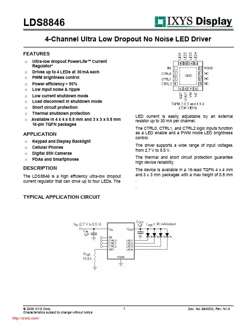
4-Channel Ultra Low Dropout No Noise LED DriverFEATURESo Ultra-low dropout PowerLite ™Current Regulator*o Drives up to 4LEDs at 30mA each o PWM brightness control o Power efficiency >95%o Low input noise &rippleo Low current shutdown modeo Load disconnect in shutdown mode o Short circuit protectiono Thermal shutdown protectionoAvailable in 4x 4x 0.8mm and 3x 3x 0.8mm 16-pin TQFN packagesAPPLICATIONo Keypad and Display Backlight o Cellular Phones o Digital Still Cameras oPDAs and SmartphonesDESCRIPTIONThe LDS8846is a high efficiency ultra-low dropout current regulator that can drive up to four LEDs.TheLED current is easily adjustable by an external resistor up to 30mA per channel.The CTRL0,CTRL1,and CTRL2logic inputs function as a LED enable and a PWM mode LED brightness control.The driver supports a wide range of input voltages from 2.7V to 5.5V.The thermal and short circuit protection guarantee high device reliability.The device is available in a 16-lead TQFN 4x 4mm and 3x 3mm packages with a max height of 0.8mm ..TYPICAL APPLICATION CIRCUITABSOLUTE MAXIMUM RATINGSParameterRating Unit V IN ,LEDx voltage -0.3to 6V V OUT voltage-0.3to 6V EN,CTRL0,CTRL1,CTRL2voltage V IN +0.7V V Storage Temperature Range -65to +150°C Junction Temperature Range -40to +125°C Soldering Temperature (10s)300°C ESD protection HBM2kVNOTE:Stresses listed above may cause permanent damage to thje device.Functional operation of the device at these or any other conditions beyond those indicated in the “Recommended Operating Conditions”is not impiled.Exposure to abslute maximum rating conditions for extended periods may remain possibility to affect device reliability.RECOMMENDED OPERATING CONDITIONSParameterRating Unit V IN2.7to 5.5V Ambient Temperature Range-40to +85°CELECTRICAL OPERATING CHARACTERISTICS(Over recommended operating conditions unless specified otherwise)V IN =3.6V,EN =High,T AMB =25°CNameConditionsMin Typ Max Units Quiescent Current I LED =20mA per channel 1.3 1.5mA Shutdown Current EN =0V 0.11µA R SET =24k20LED CurrentR SET =96k5mALED Current Setting Range 2.7<V IN <5.5V 230mA LED Current Accuracy To set value-83+8%LED Channel Matching (I LED MAX -I LED MIN )/(I LED MAX +I LED MIN )-53+5%Current Sink Dropout Voltage*2030mV Short Circuit Output Current Limit V OUT =0V2225mA High Input Voltage =V IN 1Leakage CurrentLow Input Voltage =0-1µA High 1.3EN,CTRL0,CTRL1,CTRL2pinsLogic Level ThresholdLow0.4V PWM frequency 100100000Hz PWM duty cycle 1100%Thermal Shutdown 150Thermal Hysteresis20°C Under Voltage Lockout (UVLO)Threshold 2.4V*)Voltage drop at led pin,at which LED current falls 10%below set valueCONTROL INPUTS FUNCTIONControl Inputs Output StatesCTRL2CTRL1CTRL0LED4LED3LED2LED1000OFF OFF OFFON001OFF OFF ON OFF010OFF ON OFF OFF011ON OFF OFF OFF100OFF OFF ON ON101OFF ON ON ON110ON ON ON ON111OFF OFF OFF OFFTYPICAL CHARACTERISTICSV IN=3.6V,I OUT=104mA(4LEDs at26mA each),C IN=C OUT=1µF,Vf=3.2V,T AMB=250C Power Efficiency vs.Input Voltage LED Current vs.TemperatureLED Current vs.Input Voltage Power-Up Delay TimeV OUTI LED(4LEDs)50mA/divENPower-Down Delay TimePWM Mode (1kHz,50Duty Cycle)PWM Mode (10kHz,50Duty Cycle)PWM Mode (50kHz,50Duty Cycle)I LED Current vs.DutyCycle I LED Current Error vs.DutyCycleCRL0V OUTI LED(4LEDs)50mA/divCRL0V OUTI LED(4LEDs)50mA/divCRL0V OUTI LED(4LEDs)50mA/divENV OUTI LED(4LEDs)50mA/divPIN DESCRIPTIONPin#Name Function1EN Device Enable.2CTRL0Output Control Bit0(See Table Control Pin Function) 3CTRL1Output Control Bit1(See Table Control Pin Function) 4CTRL2Output Control Bit2(See Table Control Pin Function) 5ISET LED current setting pin6V OUT Output voltage to the LED anodes7V IN Input Voltage8-11NC No internal connect12PGND Power Ground13LED4LED4Cathode Terminal14LED3LED3Cathode Terminal15LED2LED2Cathode Terminal16LED1LED1Cathode TerminalPAD PAD Connect to GND on the PCBPIN FUNCTIONEN is a Device Enable.This pin is high impedance.There should be a pulldown resistor<100k when control signal is floating.CTRL0,CTRL1,CTRL2are Output Control Bits (See Table2)and PWM LED brightness control logic inputs.Guaranteed levels of logic high and logic low are set at1.3V and0.4V respectively.CTRL0and CTRL1pins are high impedance,and they should be pull down by resistor<100k when control signal is floating.CTRL2pin has internal pull-up resitor~100k. ISET is a LED current setting pin.Resistor R SET connected from this pin to ground controls LED current.Connect this pin to ground directly for factory preset LED current value30mA.V IN is the device supply pin.A small1μF ceramic bypass capacitor is required between the V IN pin and ground at the device.The operating input voltage range is from2.7V to5.5V.Whenever the input supply falls below the under-voltage threshold(2.2 V),all the LED channels are disabled,and the device enters shutdown mode.V OUT is the charge pump output.Connect it to the LED anodes.A small1μF ceramic bypass capacitor is required between the V OUT pin and ground near the device.GND is the current regulators ground current source. Connect this pin to the ground plane on the PCB as close to the package as possible.LED1–LED4provide the internal regulated current sink for each of the LED cathodes.These pins enter a high-impedance zero current state when the device is in shutdown mode.PAD is the exposed pad underneath the package. For best thermal performance,the tab should be soldered to the PCB and connected to the ground planeBLOCKDIAGRAMFigure 2.LDS8846Functional Block DiagramBASIC OPERATIONThe device starts operating if the EN pin is set logic HIGH and input voltage is higher that under voltage protection lockout threshold.The low dropout PowerLite ™Current regulator performs well at input voltages up to 50mV greater than the LED forward voltage significantly increasing the driver’s efficiency.Input pins EN,CTRL0,CTRL1,and CTRL2may be either logic LOW or HIGH during power-up.However,logic voltage should never exceed input voltage V IN ,and these pins should not be left float.LED Current SettingThe desired current value in each of the four LED is set by external resitor R SET connevted between I SET pin and ground..The LED current is 400times greater than the current through R SET and can be estimated (in mA)by following equation:SETSETLEDR V xI400 ,where V SET =1.2V,and R SET is its resistance in kohms.R SET value for typical I LED current is shown at the table below.ILED,mA R SET ,k ΩNearest standard 1%value 59695.3104847.5153231.6or 32.4202423.7or 24.32519.219.1301615.8or 16.2The average current value may be decreased using PWM signal applied to either CTRL0,CTRL1or CTRL2pin.The LDS8846allows modulation frequiencies in the range from 100Hz to 5kHz with duty cycles from 100%to 1%and from 5kHz to 30kHz with duty cycles from 100%to 10%.Modulation frequiencies lower than 100Hz are not recommended especialy at short duty cycles because LED flicker may be visible.If CTRL1and CTRL2pins are logic HIGH and PWM signal applies to CTRL0pin,then all four LEDS are dimming synchronously.If CTRL0and CTRL2pins are logic HIGH and PWM signal applies to CTL1pin,then LEDs from LED1to LED3are dimming,while LED4is always off.Unused LED ChannelsFor applications with only two or three LEDs,unused LED can be disabled via the appropriate CTRL pins logic states.For applications requiring 1LED only,the unused LED pins should be tied to V OUT .However,we recommend use of all channels connecting them in parallel with accordingly decreased current per channel.If one LED is used only,current per channel should be decreased four times,or this device may drive one LED with maximum current up to 120mA with all channels connected in prallel and 30mA current perchennel.Figure 3.Application circuit with threeLEDsFigure 4.Application circuit with twoLEDsFigure 5.Application circuit with twoLEDsFigure 5.Application circuit with one LED Protection ModeThe LDS8846limits output current if V OUT pin is shorted to ground either before or after device start.This is to prevent the device from overload in case of short circuit at the output.Device resumes normal operation after short removed.If the die temperature exceeds +150°C,the driver will enter thermal protection shutdown mode.When the device temperature drops by about 20°C,the device resumes normal operation.If the input voltage is below under-voltage protection threshold,device turns into shutdown mode with high impedance state at V OUT and all LED pins.LED SelectionLEDs with forward voltages (V F )ranging from 1.3V to 4.5V may be used.The device exhibits the highest efficiency when V F voltage is close to V IN .If the voltage source is a Li-ion battery,we recommend selecting LEDs with V F at least 50mV below minimum expected battery discharging voltage to extend the battery life and achieve highest efficiency.If the minimum battery discharging voltage is limited at 3V,recommended V F voltage is V F =3.0–0.05=2.95VExternal ComponentsThe driver requires only one external component –current setting resistor R SET .However,if device is connected to the voltage source (battery)through long traces,or voltage source has high electrical noise due bad performance of other components connected to this source,we recommend 1uF decoupling capacitors at the V IN and V OUT pins located as close to he device as possible.Power dissipates on R SET resistor is less then 100µW that allows use of very small surface mount component.Recommended LayoutIt is recommended to minimize trace length todecoupling capacitors.A ground plane should coverthe area under the driver IC as well as the bypasscapacitors.Short connection to ground on capacitorsC IN and C OUT can be implemented with the use ofmultiple vias.A copper area matching the TQFNexposed pad(PAD)must be connected to the groundplane underneath.The use of multiple via improvesthe package heat dissipation.Figure6.LDS8846Recommended layoutPACKAGE DRAWING AND DIMENSIONS 16-PIN TQFN,3mm x3mm,0.5mm PITCHSYMBOL MIN NOM MAX A0.700.750.80A10.000.020.05A20.1780.2030.228b0.200.250.30D 2.95 3.00 3.05D1 1.65 1.70 1.75E 2.95 3.00 3.05E1 1.65 1.70 1.75e0.50typL0.3250.3750.425m0.150typn0.225typNote:1.All dimensions are in millimetersplies with JEDEC Standard MO-22016-PIN TQFN,4mm x4mm,0.65mm PITCHSYMBOL MIN NOM MAXA0.700.750.80A10.000.020.05A20.1780.2030.228b0.280.330.38D 3.90 4.00 4.10D1 2.35 2.40 2.45E 3.90 4.00 4.10E1 2.35 2.40 2.45e0.65typL0.550.600.65Note:3.All dimensions are in millimetersplies with JEDEC Standard MO-220分销商库存信息: IXYSLDS8846-002-T2。