产品信息_PT4207_PT4207
- 格式:pdf
- 大小:1.10 MB
- 文档页数:22
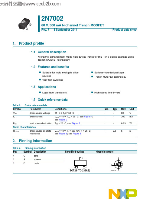
1.Product profile1.1General descriptionN-channel enhancement mode Field-Effect Transistor (FET) in a plastic package using Trench MOSFET technology.1.2Features and benefits⏹Suitable for logic level gate drive sources ⏹Very fast switching⏹Surface-mounted package ⏹Trench MOSFET technology1.3Applications⏹Logic level translators⏹High-speed line drivers1.4Quick reference data2.Pinning information2N700260 V, 300 mA N-channel Trench MOSFETRev. 7 — 8 September 2011Product data sheetTable 1.Quick reference dataSymbol ParameterConditions Min Typ Max Unit V DS drain-source voltage 25°C ≤T j ≤150°C--60V I D drain currentV GS =10V; T sp =25°C;see Figure 1; see Figure 3--300mA P tot total power dissipation T sp =25°C;see Figure 2--0.83W Static characteristicsR DSondrain-source on-state resistanceV GS =10V; I D =500mA; T j =25°C; see Figure 6; see Figure 8- 2.85ΩTable 2.Pinning information Pin Symbol Description Simplified outlineGraphic symbol1G gate SOT23 (TO-236AB)2S source 3Ddrain1233.Ordering information4.Marking[1]% = placeholder for manufacturing site code5.Limiting valuesTable 3.Ordering informationType numberPackage NameDescriptionVersion 2N7002TO-236ABplastic surface-mounted package; 3 leadsSOT23Table 4.Marking codesType numberMarking code [1]2N700212%Table 5.Limiting valuesIn accordance with the Absolute Maximum Rating System (IEC 60134).Symbol ParameterConditions Min Max Unit V DS drain-source voltage 25°C ≤T j ≤150°C-60V V DGR drain-gate voltage 25°C ≤T j ≤150°C; R GS =20k Ω-60V V GS gate-source voltage -3030V V GSM peak gate-source voltage pulsed; t p ≤50µs; δ=0.25-4040V I Ddrain currentV GS =10V; T sp =25°C;see Figure 1; see Figure 3-300mA V GS =10V; T sp =100°C; see Figure 1-190mA I DM peak drain current pulsed; t p ≤10µs; T sp =25°C;see Figure 3- 1.2A P tot total power dissipation T sp =25°C;see Figure 2-0.83W T j junction temperature -65150°C T stg storage temperature -65150°C Source-drain diodeI S source current T sp =25°C-300mA I SMpeak source currentpulsed; t p ≤10µs; T sp =25°C - 1.2A6.Thermal characteristicsTable 6.Thermal characteristicsSymbol Parameter ConditionsMin Typ Max Unit R th(j-a)thermal resistance from junction to ambientMounted on a printed-circuit board; minimum footprint ; vertical in still air--350K/WR th(j-sp)thermal resistance from junction to solder pointsee Figure 4--150K/W7.CharacteristicsTable 7.CharacteristicsSymbol Parameter Conditions Min Typ Max Unit Static characteristicsV(BR)DSS drain-sourcebreakdown voltage I D=10µA; V GS=0V; T j=25°C60--V I D=10µA; V GS=0V; T j=-55°C55--VV GSth gate-source thresholdvoltage I D=0.25mA;V DS=V GS; T j=25°C;see Figure 9; see Figure 1012 2.5VI D=0.25mA;V DS=V GS; T j=150°C;see Figure 9; see Figure 100.6--VI D=0.25mA;V DS=V GS; T j=-55°C;see Figure 9; see Figure 10-- 2.75VI DSS drain leakage current V DS=48V;V GS=0V; T j=25°C-0.011µAV DS=48V;V GS=0V; T j=150°C--10µA I GSS gate leakage current V GS=15V; V DS=0V; T j=25°C-10100nAV GS=-15V;V DS=0V; T j=25°C-10100nAR DSon drain-source on-stateresistance V GS=10V; I D=500mA; T j=25°C;see Figure 6; see Figure 8- 2.85ΩV GS=10V; I D=500mA; T j=150°C;see Figure 6; see Figure 8--9.25ΩV GS=4.5V;I D=75mA;T j=25°C;seeFigure 6; see Figure 8- 3.8 5.3ΩDynamic characteristicsC iss input capacitance V DS=10V;f=1MHz;V GS=0V;T j=25°C -3150pFC oss output capacitance- 6.830pF C rss reverse transfercapacitance- 3.510pFt on turn-on time V GS=10V; V DS=50V;R L=250Ω;R G(ext)=50Ω; R GS=50Ω- 2.510nst off turn-off time-1115ns Source-drain diodeV SD source-drain voltage I S=300mA;V GS=0V;T j=25°C;seeFigure 11-0.85 1.5VQ r recovered charge V GS=0V;I S=300mA;dI S/dt=-100A/µs -30-nCt rr reverse recovery time-30-ns8.Package outlinePlastic surface-mounted package; 3 leads SOT23Fig 13.Package outline SOT23 (TO-236AB)9.Soldering10.Revision historyTable 8.Revision historyDocument ID Release date Data sheet status Change notice Supersedes2N7002 v.720110908Product data sheet-2N7002 v.6 Modifications:•The format of this data sheet has been redesigned to comply with the new identity guidelinesof NXP Semiconductors.•Legal texts have been adapted to the new company name where appropriate.2N7002 v.620060428Product data sheet2N7002 v.52N7002 v.520051115Product data sheet2N7002 v.42N7002 v.420050426Product data sheet2N7002 v.32N7002 v.320000727Product specification HZG3362N7002 v.22N7002 v.219970617Product specification2N7002 v.12N7002 v.119901031Product specification--11.Legal information11.1Data sheet status[1]Please consult the most recently issued document before initiating or completing a design.[2]The term 'short data sheet' is explained in section "Definitions".[3]The product status of device(s) described in this document may have changed since this document was published and may differ in case of multiple devices. The latest productstatus information is available on the Internet at URL .11.2DefinitionsPreview — The document is a preview version only. The document is still subject to formal approval, which may result in modifications or additions. NXP Semiconductors does not give any representations or warranties as to the accuracy or completeness of information included herein and shall have no liability for the consequences of use of such information.Draft — The document is a draft version only. The content is still under internal review and subject to formal approval, which may result in modifications or additions. NXP Semiconductors does not give any representations or warranties as to the accuracy or completeness of information included herein and shall have no liability for the consequences of use of such information.Short data sheet — A short data sheet is an extract from a full data sheet with the same product type number(s) and title. A short data sheet is intended for quick reference only and should not be relied upon to contain detailed and full information. For detailed and full information see the relevant full data sheet, which is available on request via the local NXP Semiconductors sales office. In case of any inconsistency or conflict with the short data sheet, the full data sheet shall prevail.Product specification — The information and data provided in a Product data sheet shall define the specification of the product as agreed between NXP Semiconductors and its customer, unless NXP Semiconductors and customer have explicitly agreed otherwise in writing. In no event however, shall an agreement be valid in which the NXP Semiconductors product is deemed to offer functions and qualities beyond those described in the Product data sheet.11.3DisclaimersLimited warranty and liability — Information in this document is believed to be accurate and reliable. However, NXP Semiconductors does not give any representations or warranties, expressed or implied, as to the accuracy or completeness of such information and shall have no liability for the consequences of use of such information.In no event shall NXP Semiconductors be liable for any indirect, incidental, punitive, special or consequential damages (including - without limitation - lost profits, lost savings, business interruption, costs related to the removal or replacement of any products or rework charges) whether or not such damages are based on tort (including negligence), warranty, breach of contract or any other legal theory.Notwithstanding any damages that customer might incur for any reason whatsoever, NXP Semiconductors’ aggregate and cumulative liability towards customer for the products described herein shall be limited in accordance with the Terms and conditions of commercial sale of NXP Semiconductors.Right to make changes — NXP Semiconductors reserves the right to make changes to information published in this document, including without limitation specifications and product descriptions, at any time and without notice. This document supersedes and replaces all information supplied prior to the publication hereof.Suitability for use — NXP Semiconductors products are not designed, authorized or warranted to be suitable for use in life support, life-critical or safety-critical systems or equipment, nor in applications where failure or malfunction of an NXP Semiconductors product can reasonably be expected to result in personal injury, death or severe property or environmental damage. NXP Semiconductors accepts no liability for inclusion and/or use of NXP Semiconductors products in such equipment or applications and therefore such inclusion and/or use is at the customer’s own risk.Quick reference data — The Quick reference data is an extract of the product data given in the Limiting values and Characteristics sections of this document, and as such is not complete, exhaustive or legally binding.Applications — Applications that are described herein for any of these products are for illustrative purposes only. NXP Semiconductors makes no representation or warranty that such applications will be suitable for the specified use without further testing or modification.Customers are responsible for the design and operation of their applications and products using NXP Semiconductors products, and NXP Semiconductors accepts no liability for any assistance with applications or customer product design. It is customer’s sole responsibility to determine whether the NXP Semiconductors product is suitable and fit for the customer’s applications and products planned, as well as for the planned application and use of customer’s third party customer(s). Customers should provide appropriate design and operating safeguards to minimize the risks associated with their applications and products.NXP Semiconductors does not accept any liability related to any default, damage, costs or problem which is based on any weakness or default in the customer’s applications or products, or the application or use by customer’s third party customer(s). Customer is responsible for doing all necessary testing for the customer’s applications and products using NXP Semiconductors products in order to avoid a default of the applications and the products or of the application or use by customer’s third partycustomer(s). NXP does not accept any liability in this respect.Limiting values — Stress above one or more limiting values (as defined in the Absolute Maximum Ratings System of IEC 60134) will cause permanent damage to the device. Limiting values are stress ratings only and (proper) operation of the device at these or any other conditions above those given in the Recommended operating conditions section (if present) or the Characteristics sections of this document is not warranted. Constant or repeated exposure to limiting values will permanently and irreversibly affect the quality and reliability of the device.Document status [1][2] Product status [3] DefinitionObjective [short] data sheet Development This document contains data from the objective specification for product development. Preliminary [short] data sheet Qualification This document contains data from the preliminary specification.Product [short] data sheet Production This document contains the product specification.Terms and conditions of commercial sale — NXP Semiconductors products are sold subject to the general terms and conditions of commercial sale, as published at /profile/terms, unless otherwise agreed in a valid written individual agreement. In case an individual agreement is concluded only the terms and conditions of the respective agreement shall apply. NXP Semiconductors hereby expressly objects to applying the customer’s general terms and conditions with regard to the purchase of NXP Semiconductors products by customer.No offer to sell or license — Nothing in this document may be interpreted or construed as an offer to sell products that is open for acceptance or the grant, conveyance or implication of any license under any copyrights, patents or other industrial or intellectual property rights.Export control — This document as well as the item(s) described herein may be subject to export control regulations. Export might require a prior authorization from national authorities.Non-automotive qualified products — Unless this data sheet expressly states that this specific NXP Semiconductors product is automotive qualified, the product is not suitable for automotive use. It is neither qualified nor tested in accordance with automotive testing or application requirements. NXP Semiconductors accepts no liability for inclusion and/or use ofnon-automotive qualified products in automotive equipment or applications.In the event that customer uses the product for design-in and use in automotive applications to automotive specifications and standards, customer (a) shall use the product without NXP Semiconductors’ warranty of the product for such automotive applications, use and specifications, and (b) whenever customer uses the product for automotive applications beyond NXP Semiconductors’ specifications such use shall be solely at customer’s own risk, and (c) customer fully indemnifies NXP Semiconductors for any liability, damages or failed product claims resulting from customer design and use of the product for automotive applications beyond NXP Semiconductors’ standard warranty and NXP Semiconductors’ product specifications. 11.4TrademarksNotice: All referenced brands, product names, service names and trademarks are the property of their respective owners.Adelante, Bitport, Bitsound, CoolFlux, CoReUse, DESFire, EZ-HV, FabKey, GreenChip, HiPerSmart, HITAG, I²C-bus logo, ICODE, I-CODE, ITEC, Labelution, MIFARE, MIFARE Plus, MIFARE Ultralight, MoReUse, QLPAK, Silicon Tuner, SiliconMAX, SmartXA, STARplug, TOPFET, TrenchMOS, TriMedia and UCODE — are trademarks of NXP B.V.HD Radio and HD Radio logo — are trademarks of iBiquity Digital Corporation.12.Contact informationFor more information, please visit: For sales office addresses, please send an email to: salesaddresses@13.Contents1Product profile. . . . . . . . . . . . . . . . . . . . . . . . . . .11.1General description . . . . . . . . . . . . . . . . . . . . . .11.2Features and benefits. . . . . . . . . . . . . . . . . . . . .11.3Applications . . . . . . . . . . . . . . . . . . . . . . . . . . . .11.4Quick reference data . . . . . . . . . . . . . . . . . . . . .12Pinning information. . . . . . . . . . . . . . . . . . . . . . .13Ordering information. . . . . . . . . . . . . . . . . . . . . .24Marking. . . . . . . . . . . . . . . . . . . . . . . . . . . . . . . . .25Limiting values. . . . . . . . . . . . . . . . . . . . . . . . . . .26Thermal characteristics . . . . . . . . . . . . . . . . . . .47Characteristics. . . . . . . . . . . . . . . . . . . . . . . . . . .58Package outline. . . . . . . . . . . . . . . . . . . . . . . . . .89Soldering . . . . . . . . . . . . . . . . . . . . . . . . . . . . . . .910Revision history. . . . . . . . . . . . . . . . . . . . . . . . .1011Legal information. . . . . . . . . . . . . . . . . . . . . . . .1111.1Data sheet status . . . . . . . . . . . . . . . . . . . . . . .1111.2Definitions. . . . . . . . . . . . . . . . . . . . . . . . . . . . .1111.3Disclaimers. . . . . . . . . . . . . . . . . . . . . . . . . . . .1111.4Trademarks. . . . . . . . . . . . . . . . . . . . . . . . . . . .1212Contact information. . . . . . . . . . . . . . . . . . . . . .12Please be aware that important notices concerning this document and the product(s)described herein, have been included in section ‘Legal information’.© NXP B.V.2011.All rights reserved.For more information, please visit: For sales office addresses, please send an email to: salesaddresses@。


TNC 620 HSCIGen 3驱动器镗铣类机床的紧凑型数控系统面向机床制造商07/2021TNC数控系统带驱动系统一般信息TNC 620•铣、钻和镗机床的紧凑型数控系统•轴数:8个控制环,其中2个可配置为主轴•用海德汉变频器系统并优选使用海德汉电机•全数字化HSCI接口和EnDat接口•尺寸紧凑•CF闪存卡•海德汉Klartext对话式和G代码(ISO)编程•标准铣、钻和镗加工循环•测头探测循环•程序段处理速度快(1.5 ms)19英寸显示屏(纵向)版•一体化的显示屏、键盘和主机(MC8410)•显示器下端为键盘•多点触摸式操作15英寸显示屏(横向)版•一体化的显示屏和主机(MC8420)•独立的键盘单元•多点触控操作系统测试海德汉数控系统、功率模块、电机和编码器通常是完整系统的组成部件。
因此,需要综合测试整个系统,而不能仅仅测试各单独设备的技术性能。
损耗件海德汉数控系统中含易损件,例如、后备电池和风扇。
标准本产品遵循的标准(ISO,EN等),请见样本中的标注。
注意Intel、Intel Xeon、Core和Celeron是Intel Corporation的注册商标。
有效性本文所述功能和技术参数适用于以下数控系统和NC数控软件版本:TNC 620,NC数控软件版本817600-08(需出口许可证)817601-08(无需出口许可证)本样本是以前样本的替代版,所有以前版本均不再有效。
如有变更,恕不另行通知。
要求有些技术参数对机床的配置有特别要求。
请注意,有些功能还需机床制造商开发专用PLC程序。
功能安全特性(FS)如果未明确区分标准部件与FS部件(FS = 功能安全特性),所介绍的信息适用于这两类部件(例如, TE 735,TE 735 FS)。
对于带功能安全特性的部件,在其产品标识的最后带标识符“(FS)”,例如,UEC 3xx (FS)2目录TNC数控系统带驱动系统2一览表4HSCI控制部件16附件23电缆概要37技术说明44数据传输和通信73安装信息77主要尺寸79一般信息101其它海德汉数控系统103主题索引104请注意技术参数表内的页码。
23···分段存储器DSO/MSO 离线分析电源管理 硬件加速的串行解码I 2C 、SPI CAN/LIN ··矢量信号分析内核辅助FPGA 调试安全环境RS-232/UARTFlexRay ·····4您的设计中有模拟、数字和串行信号…示波器是否也应该能够处理这些信号呢?MegaZoom III 技术。
MegaZoom III 深存储器可捕获长时间内不重复的信号,并保持高采样率,可快速放大您关注的区域。
采样率和存储器深度联系紧密。
示波器的深存储器可在长时间内保持高采样率。
快速发现偶发错误。
硬件加速解码增加了捕获到疑难事件的概率。
在间歇性故障遭到客户抱怨或关系到产品质量之前,安捷伦示波器可帮助您捕获到这些问题。
混合信号触发器。
可同时触发任意组合的模拟和数字信号。
一台仪器中包含精确的模拟测量和准确的数字内容,且它们之间有时间关联。
数字通道的应用。
使用Altera 或XilinxFPGA 进行设计?使用FPGA 动态探头进行快速的内部FPGA 测量。
使用I2C 、SPI 或RS-232?使用4通道型号的模拟或数字信号来采集和解码这些串行总线。
InfiniiVision 7000系列示波器通道可更快地确定疑难问题。
创新的高分辨率显示。
InfiniiVision 7000系列示波器具有XGA显示和256级的亮度,可精确表述您正在测试的信号的模拟特征。
配备有业内最快速的更新速率,可达100000波形/秒,您可捕获关键的信号细节,察看偶发事件,而这些在传统的示波器上可能被漏掉。
模拟信号:高达1 GHz 带宽和4 GSa/s采样率数字信号:具有混合信号触发的16位定时通道捕获模拟或数字的混合信号。
比较数字信号的多个周期和较慢的模拟信号。
具有高达2 GSa/s 深存储器的16位高速定时通道。
使用定时通道来评测控制信号关系。