Ch3-6开关电容积分器
- 格式:doc
- 大小:315.38 KB
- 文档页数:9
3.10 开关电容(SC )滤波器用开关和电容来仿真电阻,构成的有源滤波器。
适于集成制造,具有精度高、价格低、使用方便灵活的特点。
此外还有:输入阻抗高、输出阻抗低、工作频率低(可达0.1Hz )、电路简单、易调节参数等优点。
缺点是:有高频噪声产生、动态范围限制在80dB 左右、高频工作频率限制大约为200kHz 。
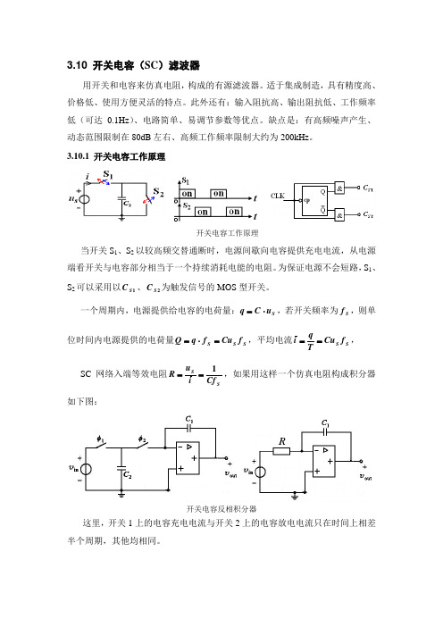
3.10.1 开关电容工作原理开关电容工作原理当开关S 1、S 2以较高频交替通断时,电源间歇向电容提供充电电流,从电源端看开关与电容部分相当于一个持续消耗电能的电阻。
为保证电源不会短路,S 1、S 2可以采用以1S C 、2S C 为触发信号的MOS 型开关。
一个周期内,电源提供给电容的电荷量:S u C q ⋅=,若开关频率为S f ,则单位时间内电源提供的电荷量S S S f Cu f q Q =⋅=,平均电流S S f Cu Tqi ==, SC 网络入端等效电阻SS Cf i u R 1==,如果用这样一个仿真电阻构成积分器如下图:开关电容反相积分器这里,开关1上的电容充电电流与开关2上的电容放电电流只在时间上相差半个周期,其他均相同。
s f C C C Cf s sRC s H S S1111)(111⋅-=⋅⋅-=-=,积分常数S f C C 11=τ,由于开关频率S f 可以调节,所以积分常数是可调的,并且积分常数由容量比决定,而不再与具体电容值有关。
在制造集成SC 滤波器时,所用到的器件(电容、电阻、开关等)均采用MOS 技术实现,简化了制造工艺,有利于提高集成度。
但是依赖于集成MOS 技术制造的电容,容量很难精确控制,误差会达到30%以上,不过依赖于同种制造工艺的电容,容量比却可以十分精确,精度可以达到0.1%以上。
因此,借助于SC 来实现电阻的集成滤波器,集成度高而且很精确。
当一个集成的通用滤波器器件内部需要用到多个SC 仿真电阻时, 每个仿真电阻都有一个S f 控制端,这样就衍生出了可编程SC 滤波器,不改变器件结构,通过编程指令改变滤波器的性能和参数。

3.10 开关电容(SC )滤波器用开关和电容来仿真电阻,构成的有源滤波器。
适于集成制造,具有精度高、价格低、使用方便灵活的特点。
此外还有:输入阻抗高、输出阻抗低、工作频率低(可达0.1Hz )、电路简单、易调节参数等优点。
缺点是:有高频噪声产生、动态范围限制在80dB 左右、高频工作频率限制大约为200kHz 。
3.10.1 开关电容工作原理开关电容工作原理当开关S 1、S 2以较高频交替通断时,电源间歇向电容提供充电电流,从电源端看开关与电容部分相当于一个持续消耗电能的电阻。
为保证电源不会短路,S 1、S 2可以采用以1S C 、2S C 为触发信号的MOS 型开关。
一个周期内,电源提供给电容的电荷量:S u C q ⋅=,若开关频率为S f ,则单位时间内电源提供的电荷量S S S f Cu f q Q =⋅=,平均电流S S f Cu Tqi ==, SC 网络入端等效电阻SS Cf i u R 1==,如果用这样一个仿真电阻构成积分器如下图:开关电容反相积分器这里,开关1上的电容充电电流与开关2上的电容放电电流只在时间上相差半个周期,其他均相同。
s f CC C Cf s sRC s H S S1111)(111⋅-=⋅⋅-=-=,积分常数S f C C 11=τ,由于开关频率S f 可以调节,所以积分常数是可调的,并且积分常数由容量比决定,而不再与具体电容值有关。
在制造集成SC 滤波器时,所用到的器件(电容、电阻、开关等)均采用MOS 技术实现,简化了制造工艺,有利于提高集成度。
但是依赖于集成MOS 技术制造的电容,容量很难精确控制,误差会达到30%以上,不过依赖于同种制造工艺的电容,容量比却可以十分精确,精度可以达到0.1%以上。
因此,借助于SC 来实现电阻的集成滤波器,集成度高而且很精确。
当一个集成的通用滤波器器件内部需要用到多个SC 仿真电阻时, 每个仿真电阻都有一个S f 控制端,这样就衍生出了可编程SC 滤波器,不改变器件结构,通过编程指令改变滤波器的性能和参数。

RDCO-01/02/03/04DDCS Communicationoption modulesOverviewThe RDCO-0x DDCS Communication options are add-on modules for the•RMIO Motor Control and I/O board (also part of RDCU control units)•BCU control units.RDCO modules are available factory-installed as well as retrofit kits.The RDCO module includes the connectors for fiber optic DDCS channels CH0, CH1, CH2 and CH3. The usage of these channels is determined by the application program; see the Firmware Manual of the drive. However, the channels are normally assigned as follows:CH0 – overriding system (eg. fieldbus adapter)CH1 – I/O options and supply unitCH2 – Master/Follower linkCH3 – PC tool (ACS800 only).There are several types of the RDCO. The difference between the types is the optical components. In addition, each type is available with a coated circuit board, this being indicated by a “C” suffix, eg. RDCO-03C.The optical components at both ends of a fiber optic link must be of the same type for the light intensity and receiver sensitivity levels to match. Plastic optical fiber (POF) cables can be used with both 5 MBd and 10 MBd optical components.10 MBd components also enable the use of Hard Clad Silica (HCS) cables, which allow longer connection distances thanks to their lower attenuation.Note: The optical component type does not reflect the actual communication speed.Delivery checkThe option package contains:•RDCO-0x module•Two screws (M3×8)•This document.Module layoutInstallationWARNING! All electrical installation andmaintenance work on the drive should be carriedout by qualified electricians only.The drive and adjoining equipment must be properly earthed.Do not work on a powered drive. Before installation, switch off the mains and other dangerous voltages (eg. from external control circuits) to the drive. After switching off the mains, always allow the intermediate circuit capacitors 5 minutes to discharge before starting work on the frequency converter. It is a good practice to check (with a voltage indicating instrument) that the drive is in fact discharged before beginning work. There may be dangerous voltages inside the drive from external control circuits even when the drive mains power is shut off. Exercise appropriate care when working on the unit. Neglecting these instructions may cause physical injury or death.WARNING! The component boards of the drivecontain integrated circuits that are extremelysensitive to electrostatic discharge (ESD). Wearan earthing wrist band when handling componentboards. Do not touch the boards unnecessarily. Do not remove any board from its antistatic packaging until required.WARNING! Handle the fiber optic cables withcare. The maximum long term tensile load is 1 N;the minimum short term bend radius is 35 mm.Do not touch the ends of the fibers with barehands as the fiber is extremely sensitive to dirt. Use rubber grommets at cable entries to protect the cables. The RDCO-0x module is to be inserted into the position marked “DDCS” on the drive. On installation, the signal and power connection to the drive is automatically made through a 20-pin connector.The module is held in place with plastic retaining clips and two screws. The screws also provide the earthing of module, and interconnect the GND signals of the module and the control board.Module TypeOptical Component TypeCH0CH1CH2CH3RDCO-01(C)10 MBd 5 MBd10 MBd10 MBd RDCO-02(C) 5 MBd 5 MBd10 MBd10 MBd RDCO-03(C) 5 MBd 5 MBd 5 MBd 5 MBd RDCO-04(C)10 MBd10 MBd10 MBd10 MBdFixingscrewsGNDFiber optic channelsCHGNDCH 0CH 1CH 2CH 3(continued overleaf)I nstallation Procedure1.Access the optional module slots on the drive. Whenevernecessary, refer to the Hardware Manual of the drive for instructions on removing any covers.2.Insert the module carefully into the slot marked with“DDCS” (BCU control unit slot 4) on the control boarduntil the retaining clips lock the module into position.3.Fasten the screws included in the package. Note thatcorrect installation of the screws is essential for fulfillingthe EMC requirements and for proper operation of themodule.4.Lead the fiber optic cables from the external device to theappropriate channel(s) of the RDCO. Inside the drive,route the cables as shown in its Hardware Manual. Make sure the cables are not kinked or laid against sharpedges. Observe colour coding so that transmitters areconnected to receivers and vice versa. In case multipledevices are to be connected to one channel, they mustbe connected in a ring.Technical dataModule types: RDCO-01(C), RDCO-02(C), RDCO-03(C), RDCO-04(C)Degree of protection: IP 20Ambient conditions: The applicable ambient conditions specified for the drive in its Hardware Manual are in effect.Connectors:•20-pin pinheader• 4 transmitter/receiver connector pairs for fiber optic cable.Type: Agilent Technologies Versatile Link. Communication speed: 1, 2 or 4 Mbit/sOperating voltage: +5 V DC ±10%, supplied by the control unit of the drive.Current consumption: 200 mA max.Electromagnetic immunity: IEC 1000-4-2 (limits: industrial, second environment); IEC 1000-4-3; IEC 1000-4-4;IEC 1000-4-6Electromagnetic emissions: EN 50081-2; CISPR 11 Dimensions (mm):349520303AFE6449229RevBEN213-4-29/drives /drivespartners。
一种推挽正激电路在低压大电流场合中,推挽电路以其结构简单、磁心利用率高的优点而得到了广泛应用。
但是,传统的推挽电路存在如下几个缺点:(1)由于原边漏感的存在,功率管关断时,漏源极产生较大的电压尖峰;(2)输入电流纹波的安秒积分大,因而输入滤波器的体积较大。
本文在传统推挽电路的基础上增加了一个箝位电容C,得到如图1所示的新型推挽正激电路拓扑。
该电路可以解决上文所述的传统电路存在的两个缺点。
图1:新型推挽正激电路拓扑2. 推挽正激电路工作原理如图1所示为推挽正激变换器。
该变换器的两个主功率开关管V1、V2和两个匝数均为Wp的初级绕组Tp1、 Tp2交替连接成一个回路,在回路的两个中点之间连接一个箝位电容C。
Cin为输入电容, Dv1 、Dv2为V1 、V2寄生的反并二极管。
D1、D2组成双半波整流电路。
电源正→原边绕组Tp2→箝位电容C→原边绕组Tp1→电源负构成一个回路。
忽略变压器漏感则加在变压器原边两个绕组的电压之和为零,箝位电容上的电压为Uin ,下正上负。
另外一个回路:电源正→V1→箝位电容C→V2→电源负。
根据基尔霍夫电路定律可得:Uds1+Uds2=Uin+Uc=2Uin因此,当某一开关管导通时,另一开关管的电压被箝位在2Uin ;当两个开关管均关断时,开关管电压各为Uin。
在分析推挽正激电路工作模态前,我们做如下设定:(1)开关管V1、V2均为理想器件,整流二极管D1、D2为理想器件,导通压降忽略不计;(2)箝位电容C较大,在工作过程中两端电压保持Uin基本不变;(3)滤波电感Lf较大,在较短的时间内可以视为恒流源,电流维持不变;稳态时输出电流Io=Uo/R; (4)原边绕组匝数同为Wp,励磁电感和漏感均相同为Lm、L ,副边匝数同为Ws,匝比n=Ws/Wp;(5)开关周期Ts, V1、V2每个周期开通时间均为Ton ,V1、V2工作的占空比均为:D=Ton/Ts;图2为推挽正激电路工作原理波形图,一共分为8个工作模态。
3.10 开关电容(SC )滤波器
用开关和电容来仿真电阻,构成的有源滤波器。
适于集成制造,具有精度高、
价格低、使用方便灵活的特点。
此外还有:输入阻抗高、输出阻抗低、工作频率低(可达0.1Hz )、电路简单、易调节参数等优点。
缺点是:有高频噪声产生、动态范围限制在80dB 左右、高频工作频率限制大约为200kHz 。
3.10.1 开关电容工作原理
开关电容工作原理
当开关S 1、S 2以较高频交替通断时,电源间歇向电容提供充电电流,从电源端看开关与电容部分相当于一个持续消耗电能的电阻。
为保证电源不会短路,S 1、S 2可以采用以1S C 、2S C 为触发信号的MOS 型开关。
一个周期内,电源提供给电容的电荷量:S u C q ⋅=,若开关频率为S f ,则单位时间内电源提供的电荷量S S S f Cu f q Q =⋅=,平均电流S S f Cu T
q
i ==
, SC 网络入端等效电阻S
S Cf i u R 1
=
=,如果用这样一个仿真电阻构成积分器如下图:
开关电容反相积分器
这里,开关1上的电容充电电流与开关2上的电容放电电流只在时间上相差
半个周期,其他均相同。
s f C C C Cf s sRC s H S S
1111
)(11
1
⋅-=⋅⋅-=-
=,积分常数S f C C
11=τ,
由于开关频率S f 可以调节,所以积分常数是可调的,并且积分常数由容量比决定,而不再与具体电容值有关。
在制造集成SC 滤波器时,所用到的器件(电容、电阻、开关等)均采用MOS 技术实现,简化了制造工艺,有利于提高集成度。
但是依赖于集成MOS 技术制造的电容,容量很难精确控制,误差会达到30%以上,不过依赖于同种制造工艺的电容,容量比却可以十分精确,精度可以达到0.1%以上。
因此,借助于SC 来实现电阻的集成滤波器,集成度高而且很精确。
当一个集成的通用滤波器器件内部需要用到多个SC 仿真电阻时, 每个仿真电阻都有一个S f 控制端,这样就衍生出了可编程SC 滤波器,不改变器件结构,通过编程指令改变滤波器的性能和参数。
3.10.2 寄生电容问题
在SC 集成滤波器中,MOS 开关和电容的每个端子到地都有寄生电容存在,寄生电容的容量无法准确估计,有时寄生电容容量可以达到电容本身的10%,设计器件时应当尽量避免寄生电容对滤波器的性能及参数造成影响。
SC 反相积分器的寄生电容分布
1p C —开关S 1对地的寄生电容;
2p C —开关S 1、开关S 2、电容C 2的上极板对地寄生电容; 3p C —电容C 2下极板对地的寄生电容;
4p C —S 2和C 1上极板对地的寄生电容;5p C —C 1下极板对地寄生电容。
其中1p C 、3p C 、5p C 分别与输入电压源、短路线、输出端并联,对转移函
数无影响。
4p C 连接在“虚地”之间,在不考虑运放的非理想因素时,也无影响。
而2p C 与C 2并联,将影响积分常数。
1. 对寄生电容不敏感的反相积分器
对寄生电容不灵敏的反相积分器
与前例电路相似的由制造S 1、C 1、C 2带来的寄生电容因为不影响积分常数,
所以未画出,图中只画出了由开关改造带来的新寄生电容21p p C C ''、,可见寄生电容21p p C C ''、对电容C 2的充电路径(S 1闭合时)和放电路径(S 2闭合时)均不产生影响,所以也不影响转移函数。
2. 对寄生电容不敏感的同相积分器——开关位置与反相积分器不同。
对寄生电容不灵敏的同相积分器
对积分环节而言,SC 构成的仿真电阻
R f C R S -=-=21等效,S f sC C C R s s H 1
2
1)(1)(=--=
3. 差分积分器
可以使用叠加定理分析。
V 1单独作用时,V 2=0,积分器为反相积分;当V 2
单独作用时,V 1 =0,积分器是同相积分。
所以,
)()(121
2112212V V f sC C
V f sC C V f sC C s H S S S -=⋅-⋅=
4. 开关电容二阶通用滤波器
等效电路
其中1111111C K f C K R S '==
,1414411C K f C K R S '==,25
2551
1C K f C K R S '-=-=- ②节点:0)1()1(
31164
121=++++V sC C sK R V C sK R V o in ④节点:
02235
3
=++-o in V sC V C sK R V
2
54562
2
515223545
62
515
2234
65
21
253
2
1)(S S S S in o f K K f K K s s f K K f K K s s K K K K K s s K K K K s s K K K s K s K K s K K s V V s H +⋅++⋅+-=''+'⋅+''+'⋅+-='+⋅+''+⋅+'-==
式中K 参数均为电容比值,滤波器特征参数只与电容比有关。
540K K f S =ω,
4
565456560
1,
K K K K K K K Q K K f Q
S ===ω,通过适当设计1K 、2K 、3K 可以实现不同种类的滤波器。
3.10.3 通用SC 滤波器
基本组成:运放级、求和级、两个SC 积分器(积分常数K 可以由时钟频率控制),内置开关S (可以由外部控制)。
有2个输入端子,3个输出端子。
通用集成SC 滤波器通过适当的外部连接可以实现各种不同的滤波特性。
使用非常灵活。
以外接反馈环路的不同分三种工作模式来讨论。
1. 工作模式一:从V 3、V 5引入到运放输入端的反馈,同时从V 6接负反馈到求和级。
2. 工作模式二:在模式一的基础上,再增加从V
到运放输入端的反馈。
6
3. 工作模式三:在工作模式二基础上去掉求和级反馈。
4. 工作模式四:改变输入信号接法
例:分析工作模式4—(1)的转移函数。
5
64
56345
32123V s
K V V s K
V V V V V V R R
V R R V in in ==--=--=→
BPF
)1(
)(LPF
)1(
)(2
3
221
2
552
3
222
1
2
66⇒⇒+⋅++⋅-==⇒⇒+⋅++-==K K R R s s K
R R s V V s H K K R R s s K R R V V s H in
in
⎥⎥
⎥⎥
⎥⎦
⎤⎢⎢⎢⎢⎢⎣⎡+⋅++⎥⎦⎤⎢⎣⎡+-+-=+⋅++⋅-⋅--==2
3222
12313221
2
2
3
2212321233)1()1()(K K R R s s K Ks R R R R R R s R R
K K R R s s K
R R
s R R R R V V s H in 当32123132)1(R R R R R R R R -=⎥⎦
⎤⎢⎣⎡+-时,即:122
12--=R R 时,可以实现APF 。