四川永星厚膜片式电阻器选型手册
- 格式:pdf
- 大小:419.68 KB
- 文档页数:2
贴片电阻详细信息:类型参考国际的分类常规系列厚膜贴片电阻General purpose General purpose, 0201 - 0805General purpose, 1206 - 2512高精度高稳定性贴片电阻High precision - high stability High precision - high stability, 0201 - 0603 High precision - high stability, 0805 - 1210High precision - high stability, 2010 - 2512高精密贴片电阻- AR 系列的特性与用途-超精密性±0.01% ~ ±1%-TaN 和NiCr 真空溅镀-温度系数只有±5PPM/°C ~ ±50PPM/°C-Wide R-Value range-Products with Pb-free Terminations Meet RoHS Requirments常应用于-医疗设备-精密量测仪器-电子通讯,转换器,印表机-Automatic Equipment Controller-Communication Device, Cell phone, GPS, PDA-一般消费性产品常规系列薄膜贴片电阻General purpose thin film General purpose thin film, 0201-2512低阻值贴片电阻Low ohmic Low ohmic, 0402 - 1206Low ohmic, 2010 - 2512贴片电阻阵列Arrays Arrays, convex and concave贴片电流传感器SMD current sensors Current Sensors - Low TCR贴片网络电阻器Network Network, T-type and L-type另有贴片厚膜排阻,贴片打线电阻,贴片高压电阻,贴片功率电阻等!片式固定电阻器,从Chip Fixed Resistor直接翻译过来的,俗称贴片电阻(SMD Resistor),是金属玻璃铀电阻器中的一种。
No.: RPCH-K-HTS-0001 /2Date: 2017.4.21Data sheetTitle: FIXED THICK FILM CHIP RESISTORS; RECTANGULAR TYPE AND HIGH POWER ⋅ ANTI SURGEStyle: RPCH16,20,32,35AEC-Q200 qualifiedRoHS COMPLIANCE ITEMHalogen and Antimony FreeNote: ・Stock conditionsTemperature: +5°C ∼+35°CRelative humidity: 25% ∼ 75%The period of guarantee: Within 2 year from shipmen t by the company.Solderability shall be satisfied.・Product specification contained in this data sheetare subject to change at any time without notice・If you have any questions or a Purchasing Specification for any quality Agreement is necessary, please contact our sales staff. ArrayHokkaido Research CenterApproval by: T. SannomiyaDrawing by: M. Shibuya1. Scope1.1 This data sheet covers the detail requirements for fixed thick film chip resistors; rectangular type & high power ⋅ anti surge,style of RPCH16,20,32,35.1.2 Applicable documentsJIS C 5201−1: 2011, JIS C 5201−8: 2014, JIS C 5201−8−1: 2014 IEC60115−1: 2008, IEC60115−8: 2009, IEC60115−8−1: 2014 EIAJ RC −2134C −20102. ClassificationType designation shall be the following form.(Example) RPCH 32 K 123 J TP 1 2 3 4 5 6 Style1 Fixed thick film chip resistors; rectangular type & & high power ⋅ anti surge2 Rated dissipation and / or dimension3 T emperature coefficient of resistance4 Rated resistance123 E24 Series, 3 digit, Ex. 123--> 12k Ω, 1000 E96 Series, 4 digit, Ex. 1000-->100Ω1022--> 10.2k Ω5 T olerance on rated resistanceD ±0.5% F ±1% J ±5%6 Packaging formB Bulk (loose package) TP Paper taping TE Embossed tapingK ±100×10−6/ °C−(Dash ) Standard Style3. Rating3.1 The ratings shall be in accordance with T able −1.T able −1StyleRated dissipation (W) T emperature coefficient of resistance (10-6 / °C) Rated resistance range (Ω)Preferred number series for resistors T olerance on rated resistance RPCH160.33K ±100 10∼1M E24, 96 D(±0.5%), F(±1%) Standard ±200 1.0∼9.76 K ±100 10∼1M E24 J(±5%) Standard ±200 1.0∼9.1 RPCH20 0.5K ±100 10∼1M E24, 96 D(±0.5%), F(±1%) Standard ±200 1.0∼9.76 K ±100 10∼1M E24 J(±5%) Standard ±200 1.0∼9.1 RPCH32 0.66K ±100 10∼1M E24, 96 D(±0.5%), F(±1%) Standard ±200 1.0∼9.76 K ±100 10∼1M E24 J(±5%) Standard ±200 1.0∼9.1 RPCH35 0.75K ±100 10∼1M E24, 96 D(±0.5%), F(±1%) Standard ±200 1.0∼9.76 K ±100 10∼1M E24J(±5%)Standard±200 1.0∼9.1Style Limiting element voltage(V) Isolation voltage(V) Category temperaturerange(°C)RPCH16 150150 −55~+155RPCH20200500RPCH32 RPCH353.2 Climatic category55/155/56 Lower category temperature − 55 °C Upper category temperature +155 °C Duration of the damp heat, steady state test 56days 3.3 Stability class5% Limits for change of resistance:−for long −term tests ±(5%+0.1Ω) −for short −term tests ±(1%+0.05Ω)3.4 DeratingFigure–1 Derating curveAmbient temperature (°C)3.5 Rated voltaged.c.or a.c.r.m.s.voltage calculated from the square root of the product of the rated resistance and the rated dissipation. E: Rated voltage (V)E =P ·RP: Rated dissipation (W) R: Rated resistance (Ω)Limiting element voltage can only be applied to resistors when the resistance value is equal to or higher than the criticalresistance value.At high value of resistance, the rated voltage may not be applicable.4. Packaging formThe standard packaging form shall be in accordance with T able −2.T able −2Symbol Packaging form Standard packagingquantity / unitsApplicationB Bulk (loose package) 1,000 pcs .RPCH16,20,32,35 TP Paper taping 8mm width, 4mm pitches 5,000 pcs. RPCH16,20,32TE Embossed taping8mm width, 4mm pitches 4,000 pcs. RPCH355. Dimensions5.1 The resistor shall be of the design and physical dimensions in accordance with Figure −2 and T able −3.Figure −2T able −3 Unit: mmStyle L W H c d RPCH16 1.6±0.1 +0.15 0.8 -0.05 0.45±0.10 0.3±0.2 0.3±0.1 RPCH20 2.0±0.1 1.25±0.10 0.55±0.10 0.3±0.2 0.4±0.2 RPCH32 3.1±0.1 1.6±0.15 0.55±0.10 0.4±0.25 0.5±0.25 RPCH35 3.1±0.15 2.5±0.15 0.55±0.15 0.4±0.25 0.5±0.255.2 Net weight (Reference)Style Net weight(mg) RPCH16 2 RPCH20 5 RPCH32 9 RPCH35 166. MarkingResistorThe Rated resistance shall be marked in 3 digits (E24) or 4 digits (E96) and marked on over coat side.• E24 series: 3 digits, E96 series: 4 digitsIn case of the resistance value that E96 overlaps with E24, It is marked by either.The Rated resistance of RPCH16 should not be marked in 4 digits(E96)Marking example Contents Application123 12×10 3 [Ω]→ 12 [kΩ]E24(RPCH16,20,32,35)2R2 2. 2[Ω]E24(RPCH 16,20,32,35)5623 562 ×103 [Ω] → 562 [kΩ] E96(RPCH 20,32,35)12R7 12.7 [Ω] E96(RPCH 20,32,35)7. Performance7.1 The standard condition for tests shall be in accordance with Sub−clause 4.2, JIS C 5201−1: 2011.7.2 The performance shall be satisfied in T able−4.T able−4(1)No. T est items Condition of test (JIS C 5201−1) Performance requirements1 Visual examination Sub−clause 4.4.1Checked by visual examination. As in 4.4.1The marking shall be legible, as checked by visual examination.2 DimensionResistance Sub−clause 4.4.2Sub−clause 4.5As specified in T able−3 of thisspecification.As in 4.5.2The resistance value shallcorrespond with the rated resistancetaking into account the specifiedtolerance.3 Voltage proof Sub−clause 4.7Method: 4.6.1.4T est voltage: Alternating voltage with a peakvalue of 1.42 times the insulationvoltage.Duration: 60 s ± 5 sInsulation resistanceT est voltage: Insulation voltageDuration: 1 min. No breakdown or flash over R ≥ 1 G Ω4 Solderability Sub−clause 4.17Without ageingFlux: The resistors shall be immersed in anon−activated soldering flux for 2s.Bath temperature: 235 °C ± 5 °CImmersion time: 2 s ± 0.5 s As in 4.17.4.5The terminations shall be covered with a smooth and bright solder coating.T able −4(2)No T est items Condition of test (JIS C 5201−1)Performance requirements 5Mounting Overload (in the mounted state) Solvent resistance of the marking Sub −clause 4.31 Substrate material: Epoxide woven glass Sub −clause 4.13 The applied voltage shall be 2.5 times the rated voltage or twice the limiting element voltage, whichever is the less severe. Duration: 2 s Visual examination ResistanceSub −clause 4.30 Solvent: 2−propanolSolvent temperature: 23 °C ± 5 °C Method 1Rubbing material: cotton wool Without recoveryNo visible damage ∆R ≤ ± (1%+0.05Ω) Legible marking6Mounting Bound strength of the end face plating Final measurements Sub −clause 4.31 Substrate material: Epoxide woven glass Sub −clause 4.33 Bent value: 3 mm Resistance Sub −clause 4.33.6 Visual examination∆R ≤ ± (1%+0.05Ω) No visible damage7Resistance to soldering heat Component solvent resistance Sub −clause 4.18 Solder temperature: 260 °C ± 5 °C Immersion time: 10 s ± 0.5 s Visual examination Resistance Sub −clause 4.29 Solvent: 2−propanolSolvent temperature: 23 °C ± 5 °C Method 2Recovery: 48 h Visual examination ResistanceAs in 4.18.3.4No sign of damage such as cracks. ∆R ≤ ± (1%+0.05Ω)No visible damage ∆R ≤ ± (1%+0.05Ω)T able −4(3)No T est itemsCondition of test (JIS C 5201−1)Performance requirements 8MountingAdhesionRapid change temperatureSub −clause 4.31Substrate material: Epoxide woven glass Sub −clause 4.32 Force: 5 NDuration: 10 s ± 1 s Visual examination Sub −clause 4.19Lower category temperature:−55 °C Upper category temperature:+155 °CDuration of exposure at each temperature: 30 min.Number of cycles: 5 cycles. Visual examination ResistanceNo visible damageNo visible damage ∆R ≤ ±(1%+0.05Ω) 9Climatic sequence −Dry heat−Damp heat, cycle (12+12hour cycle) First cycle−Cold−Damp heat, cycle (12+12hour cycle) Remaining cycle−D.C. loadSub −clause 4.23 Sub −clause 4.23.2T est temperature: +155 °C Duration: 16 h Sub −clause 4.23.3 T est method: 2T est temperature: 55 °C [Severity(2)]Sub −clause 4.23.4T est temperature −55 °C Duration: 2hSub −clause 4.23.6 T est method: 2T est temperature: 55 °C [Severity (2)]Number of cycles: 5 cycles Sub −clause 4.23.7The applied voltage shall be the rated voltage or the limiting element voltage whichever is the smaller.Duration: 1 min. Visual examination ResistanceNo visible damage ∆R ≤ ± (5%+0.1Ω) 10MountingEndurance at 70 °C Sub −clause 4.31Substrate material: Epoxide woven glass Sub −clause 4.25.1Ambient temperature: 70 °C ± 2 °C Duration: 1000 hThe voltage shall be applied in cycles of 1.5 h on and 0.5 h.The applied voltage shall be the rated voltage or the limiting element voltage whichever is the smaller.Examination at 48 h , 500 h and 1000 h:Visual examination ResistanceNo visible damage ∆R ≤ ± (5%+0.1Ω)T able −4(4)No T est items Condition of test (JIS C 5201−1)Performance requirements 11Mounting V ariation of resistance with temperature Sub −clause 4.31 Substrate material: Epoxide woven glass Sub −clause 4.8 −55 °C / +20 °C+20 °C / +155°CAs in T able −112Mounting Damp heat, steady state Sub −clause 4.31 Substrate material: Epoxide woven glass Sub −clause 4.24Ambient temperature: 40 °C ± 2 °C +2 Relative humidity : 93 % −3 a) 1st group: without voltage applied.b) 2nd group: The d. c. voltage shall be appliedcontinuously .The voltage shall be accordance with Sub −clause 4.24.2.1 b). without polarizing voltage [4.24.2.1, c)] Visual examinationResistanceNo visible damage Legible marking ∆R ≤ ± (5%+0.1Ω) 13Dimensions (detail) Mounting Endurance at upper category temperature Sub −clause 4.4.3 Sub −clause 4.31 Substrate material: Epoxide woven glass Sub −clause 4.25.3 Ambient temperature:155 °C ± 2 °CDuration: 1000 hExamination at 48 h, 500 h and 1000 h:Visual examination Resistance As in T able −3No visible damage ∆R ≤ ± (5%+0.1Ω)8. T aping8.1 Applicable documents JIS C 0806−3: 2014, EIAJ ET −7200C: 2010 8.2 T aping dimensions8.2.1 T aping dimensions shall be in accordance with Figure −3 and T able −5.Unit: mmFigure −3T able −5 Unit: mmStyle A B t 1 t 2 RPCH16 1.15±0.15 1.9±0.2 0.6±0.1 0.8max. RPCH20 1.65±0.15 2.5±0.2 0.8±0.1 1.0max. RPCH32 2.00±0.15 3.6±0.2 0.8±0.1 1.0max.8.2.2 Embossed taping dimensions shall be in accordance with Figure −4 and T able −6.Unit: mmFigure −4T able −6 Unit: mmStyle A B W E t 1 RPCH35 2.85±0.20 3.5±0.2 8.0±0.3 3.5±0.05 1.0±0.21). The cover tapes shall not cover the sprocket holes.2). T apes in adjacent layers shall not stick together in the packing. 3). Components shall not stick to the carrier tape or to the cover tape. 4). Pitch tolerance over any 10 pitches ±0.2mm.5). The peel strength of the top cover tape shall be with in 0.1N to 0.5N on the test method as shown in the followingRPCH16,20,32:Figure −4,RPCH35:Figure-5.6). When the tape is bent with the minimum radius for 25 mm, the tape shall not be damaged and the components shallmaintain their position and orientation in the tape.7). In no case shall there be two or more consecutive components missing.The maximum number of missing components shall be one or 0.1%, whichever is greater. 8). The resistors shall be faced to upward at the over coating side in the carrier cavity .Figure −5Figure −6/min )165°to180°Carrier tape T op cover tapeP eel −off(About 300mm /min )Direction of unreelingNo: RPCH −K −HTS −0001 /2Title:FIXED THICK FILM CHIP RESISTORS; RECTANGULAR TYPE ANDHIGH POWER ⋅ ANTI SURGE RPCH16,20,32,35Page: 10/10Product specification contained in this data sheet are subject to change at any time without notice.If you have any questions or a Purchasing Specification for any quality agreement is necessary, please contact our sales staff.Issue: KAMAYA ELECTRIC CO., LTD. Research & Development Department HOKKAIDO Research center Last update: 2017.4.218.3 Reel dimensionReel dimensions shall be in accordance with the following Figure −7 and T able −7.T able −7 Unit: mmStyleA B Note RPCH16,20,32,35 +1.0 9 011.4±1.0 Injection molding13±1.0 V acuum formingNote : Marking label shall be marked on a place of Marking A or two place of marking A and B.Figure −89. Marking on packageThe label of a minimum package shall be legibly marked with follows. 9.1 Marking A(1) Classification(Style, T emperature coefficient of resistance, Rated resistance, T olerance on rated resistance, Packaging form)(2) Quantity (3) Lot number (4) Manufacturer’s name or trade mark (5) Others9.2 Marking B (KAMA Y A control label)。

Application Note 应用指南Product Name:Chip Resistor产品名称:晶片电阻器Uniroyal Electronics Global Co., Ltd. 厚声国际贸易(昆山) 有限公司Building # 3, No. 88 Longteng Road, Economic & Technical Development Zone, Kunshan City, Jiangsu Province, China 215333 中国江苏省昆山市经济技术开发区龙腾路88号3号房TEL: +86 512 3687 3924Email: **************/CONTENT目录1SAFETY CONSIDERATION安全注意事项 (1)2USAGE CONSIDERATIONS使用注意事项 (2)3MOUNTING CONSIDERATION安装注意事项 (3)4STORAGE CONSIDERATION存储的注意事项 (7)5EXPORTATION CONSIDERATION出口注意事项 (7)6INDUSTRIAL PROPERTY PROHIBITIONS工业产权禁令 (7)7TECHNICAL GUIDANCE技术指导 (8)8OTHER MATTERS其他事项 (16)NOTES说明 (18)1Safety consideration安全注意事项1.1The products are designed and produced for application in ordinary electronic equipment (AV equipment, telecommunication equipment, home appliances amusement, etc.).If the products are to be used in devices requiring extremely high reliability (medical equipment, transport equipment, aircraft/spacecraft, nuclear power controllers, car equipment including car accessories, safety devices, etc.) and whose failure or operational error may endanger human life, please consult with the company,s Sale’s Dept. to advance.产品被设计和生产用于普通电子设备(AV设备、电信设备、家电娱乐等)。
o nl i ne c o mp*RoHS Directive 2002/95/EC Jan 27 2003 including Annex.Specifi cations are subject to change without notice.Load Life ...................................±1.00 %Moisture Resistance .................±0.50 %Resistance to Soldering Heat ...±0.25 %Thermal Shock .........................±0.25 %Physical CharacteristicsFlammability ........Conforms to UL94V-0Lead Frame Material........................Copper, solder coated Body Material ..................ThermoplasticHow To Order48 16 P - 1 - 103 __ __Model(48 = SOM Pkg.)Number of Pins Electrical Confi guration • 1 or 4 = Isolated* • 2 = Bussed*• 3 = Dual Terminator*Resistance Code• First 2 digits are signifi cant • Third digit represents the number of zeros to follow.Resistance Tolerance• Blank = ±2 % (see “Resistance Tolerance” on next page for resistance range) • F = ±1 % (100 ohms - 1 megohm) • D = ±0.5 % (100 ohms - 1 megohm)Terminations• All electrical confi gurations EXCEPT T03: LF = RoHS compliant • ONLY electrical confi guration T03: L = RoHS compliant • Blank = Tin/Lead-plated*For tube packaging, use T01, T02, T03 or T04. Consult factory for other available options.vary.For Standard Values Used inCapacitors, Inductors, and Resistors, click here .Recommended Land PatternTRADEMARKNOTE: Land pattern dimensions are based on design rules established by the Institute for Inter-connecting and Packaging Electronic Circuits in IPC-SM-782.1.27(.050).63(.025)Lead coplanarity .102mm (.004 inch) max. at mounting erning dimensions are in metric. Dimensions in parentheses are inches and are approximate.*Terminal centerline to centerline measurements made at point of emergence of the lead from the body..305 + .000/ - .101*R o H S C O M P L I A N T V E R S I O N S A V A I L A B L EMKS P/No nl i n e c o mp o ne n t s 11621531441351261171089R1R2R3R4R5R6R7R81615R81413R71211R6109R5R112R234R356R478 Specifi cations are subject to change without notice.REV . 07/10For information on specifi c applications, download Bourns’ application notes:■ DRAM Applications■ Dual Terminator Resistor Networks ■ R/2R Ladder Networks ■ SCSI ApplicationsIsolated Resistors (1 and 4 Circuits)Model 4814P-1Model 4816P-1 (Shown)Model 4818P-1 Model 4820P-1Bussed Resistors (2 Circuit)Model 4814P-2Model 4816P-2 (Shown)Model 4818P-2 Model 4820P-2Dual Terminator (3 Circuit)Model 4814P-3Model 4816P-3 (Shown)Model 4818P-3 Model 4820P-3Resistance Tolerance10 ohms to 49 ohms ..................±1 ohm 50 ohms to 2.2 megohms ............±2 %*Power Rating per Resistor1 Circuit at 70 °C ..................0.160 watt 4 Circuit at 70 °C ..................0.160 wattPopular Resistance Values (1, 4 and 2 Circuits)**OhmsCode Ohms Code Ohms Code Ohms Code Ohms Code 101001801811,80018215,000153120,000124222202202212,00020218,000183150,000154272702702712,20022220,000203180,000184333303303312,70027222,000223220,000224393903903913,30033227,000273270,000274474704704713,90039233,000333330,000334565605605614,70047239,000393390,000394686806806815,60056247,000473470,000474828208208216,80068256,000563560,0005641001011,0001028,20082268,000683680,0006841201211,20012210,00010382,000823820,0008241501511,50015212,000123100,0001041,000,000105* Add “F” after resistance code for ±1 % tolerance available from 100 Ω through 1M Ω, or add “D” after resistance code for ±0.5 % tolerance available from 100 Ω through 1M Ω.Part number suffi x examples: -103 = 10K Ω, ±2 %; -103F = 10K Ω, ±1 %; -103D = 10K Ω, ±0.5 %** Non-standard values available, within resistance range.Popular Resistance Values (3 Circuit)**ResistanceOhms CodeR 1R 2R 1R 21602401612411803901813912202702212712203302213313303903313913304703314713,0006,200302622Model 4816P-4 (Shown)Model 4820P-4Resistor Power Temp. Derating CurveResistance Tolerance10 ohms to 49 ohms ..................±1 ohm 50 ohms to 2.2 megohms ............±2 %*Power Rating per Resistor2 Circuit at 70 °C ..................0.080 wattResistor Power Temp. Derating CurveResistance Tolerance Below 100 ohms ......................±2 ohms 100 ohms to 2.2 megohms ..........±2 %*Power Rating per Resistor3 Circuit at 70 °C ..................0.080 wattResistor Power Temp. Derating CurveW A T T S 070125.225.200.175.150.125.100.075.050.02525AMBIENT TEMPERATURE (°C)W A T T SAMBIENT TEMPERATURE ( C )°070125.225.200.175.150.125.100.075.050.02525W A T T SAMBIENT TEMPERATURE ( C )°070125.225.200.175.150.125.100.075.050.02525o nl i ne c o mSpecifi cations are subject to change without notice.Electrical Confi guration *Circuit CodesExamples Tape & ReelTubes Isolated 1T014816P-1-101Bussed 2T02Isolated Circuit in Tape & Reel Package Dual Terminated 3T034816P-T01-101Adj. Isolated4T04Isolated Circuit in Slide Tube Package*4816P-X-RC: To specify package type, replace “X” with appropriate “Circuit Code”.NOTE: DIMENSIONS NOT SPECIFIED ARE PER EIA RS-481-2.DIMENSIONS:MM (IN)Model Standard Quantityper ReelCarrier Tape Width (W)Cover Tape Width(W)Reel Width(T)Pocket Center(F)4814P 2,00024.0 ± .30 (.945 ± .012) 21.0(.827) NOM. 30.4(1.197) MAX.11.5 ± .10 (.453 ± .004)4816P 4818P 4820PLeader Length = 500 min. }Empty Component Pockets Trailer Length = 500 mm min.Sealed with Cover Tape。
我们常说的贴片电阻(SMD Resistor)学名叫:片式固定电阻器,是从Chip Fixed Resistor直接翻译过来的。
特点是耐潮湿,耐高温,可靠度高,外观尺寸均匀,精确且温度系数与阻值公差小。
按生产工艺分厚膜(Thick Film Chip Resistors)、薄膜(Thin Film Chip Resistors)两种。
厚膜是采用丝网印刷将电阻性材料淀积在绝缘基体(例如玻璃或氧化铝陶瓷)上,然后烧结形成的。
我们通常所见的多为厚膜片式电阻,精度范围±0.5% ~ 10%,温度系数:±50PPM/℃~ ±400PPM/℃。
薄膜是在真空中采用蒸发和溅射等工艺将电阻性材料淀积在绝缘基体工艺(真空镀膜技术)制成,特点是低温度系数(±5PPM/℃),高精度(±0.01%~±1%)。
封装有:0201,0402,0603,0805,1206,1210,1812,2010,2512。
其常规系列的精度为5%,1%。
阻值范围从0.1欧姆到20M欧姆。
标准阻值有E24,E96系列。
功率有1/20W、1/16W、1/8W、1/10W、1/4W、1/2W、1W。
特性:体积小,重量轻适合波峰焊和回流焊机械强度高,高频特性优越常用规格价格比传统的引线电阻还便宜生产成本低,配合自动贴片机,适合现代电子产品规模化生产使用状况:由于价格便宜,生产方便,能大面积减少PCB面积,减少产品外观尺寸,现在已取代绝大部分传统引线电阻。
除一些小厂或不得不使用引线电阻的设计,各种电器上几乎都在使用。
目前绝大部分电子产品,以0603、0805器件为主;以手机,PDA为代表的高密度电子产品多使用0201、0402的器件;一些要求稳定和安全的电子产品,如医疗器械、汽车行驶记录仪、税控机则多采用1206、1210等尺寸偏大的电阻。
市场状况:目前,在全球的市场份额中,排名依次是台湾、日本、中国、韩国,欧美几乎不再生产。
Internal construction of RP Series (non-inductive serpentine film)U U U U UU U U U UIndustry’s widest range of high value/ high voltage resistors- 1/8 ~ 20W, 1K Ω~ 1013Ω, 300V~ 90KV , TC’s to ±15ppm, ±0.05%~ 10% Available on T ape & Reel (sizes <2.5” long)RCD’s high voltage thick-film resistors represent the most advanced technology in the industry. Series RG is designed for semi-precision applications, offering a low cost solution up to 15KV . Series RH features a special composition and processing to achieve improved tolerance, TC, & voltage (60KV). Series RP utilize highest grade materials enabling tightest tolerances, lowest VC’s, TC’s to 15ppm, and superior power/temp/voltage levels (90KV). RP utilize serpentine film pattern for lowest inductance. Units are printed or banded with resistance value and tolerance as minimum.The ruggedness of these models enables superior long term reliability, especially in demanding applications such as military, space, and medical equipment, as well as electron microscopes, high impedance amplifiers, electrometer, radiation testers, etc.* Maximum working voltage is DC or AC RMS (50-60Hz sinusoidal) and is determined by E= (PR)1/2, E not to exceed value listed in column above. **Consult factory for res. values outside the standard rangeOPTIONSOptions include formed leads, matched sets, custom marking, burn-in,vacuum/space operation, custom sizes, etc. Opt. P = high pulse design,Opt.H= increased voltage, Opt.B=increased power, Opt.58=hermetic seal.* Extended temperature range available ** Tinned copper leads avail. on Series RP (specify Opt.25)DERA TING100 75 50 25 025 50 75 100 125 150 175 200 225AMBIENT TEMPERATURE (°C)% R A T E D P O W E RRPRG,RHIncreased Ratings - increased power and voltage ratings are available with special processing. By specifying Opt.H on RG series, voltage ratings are increased by 100% (by 50% on sizes 2W-4W).Matched Sets and Networks - cost savings up to 50% can often be achieved by specifying tight matching requirements instead of tight tol. and TC reqts.Resistance matching to 0.02% and TC tracking to 5ppm is available.Threaded Terminations - resistors are available with tapped end caps for series combination into virtually any voltage or resis. value.Hermetic-Sealed Construction (Opt. 58) - Available on RH1, RH2, & RH3for use in harshest environments. Add .08” to dia. & .18” to length.CUSTOM DESIGNS SPECIFICATIONS (Typ.)1RH2 is available in 400ppm TCR from 100G to 300G, 300G-600G is 1000ppm, 600G-3T is 1500ppm 2 RH3 is available in 400ppm TCR from 100G-600g, 600G-1T is 1000ppm, 1T-10T is 1500ppmG R W e g a t t a e g a tl o V c i r t c e l e i D ]m m [h c n I s n o i s n e m i D 01=K (**e g n a R e c n a ts i s e R d r a d n a t S 301=M ,601=G ,9)s e i r e S C °52@*g n i t a R h t g n e r t S L Dd m pp 52m p p 05mp p 001m p p 002m p p 0538/1G R W 8/1V 003V 005]0.1±4.3[40.±431.]46.0±7.1[520.±760.]5.[020.A /N M 01-M 1M 003-M 1M 003-M 1M 003-M 14/1G R W 4/1V 005V 005]0.1±5.6[40.±652.]46.0±5.2[520.±890.]6.[420.A /N M 05-K 001G 3-K 001G 3-K 001G 3-K 0012/1G R W 2/1V K 1V 005]0.1±4.9[40.±863.]18.0±4.3[230.±431.]46.[520.A /N M 05-K 001G 3-K 001G 3-K 001G 3-K 001S 1G R W 1V K 5.1V 005]3.1±0.21[50.±274.]18.0±0.4[230.±851.]7.[820.A /N M 05-k 002M 001-K 002M 003-K 002M 003-K 0021G R W 1V K 2V K 1]3.1±8.41[50.±185.]18.0±5.5[230.±612.}8.[130.A /N M 05-k 002M 001-K 002M 005-K 002M 005-K 0022G R W 2V K 5V K 1]6.1±9.62[260.±60.1]18.0±0.7[230.±572.}8.[130.A /N A /N ****G 5.1-M 13G R W 3V K 01V K 1]6.1±4.24[260.±76.1]18.0±0.7[230.±572.}8.[130.A /N A /N ****G 5.1-M 14G R W4VK 51VK 1]6.1±1.25[260.±50.2]20.1±5.8[230.±533.]1[040.A /N A /N ****G5.1-M 1P R W e g a t t a e g a t l o V c i r t c e l e i D ]m m [h c n I s n o i s n e m i D 01=K (**e g n a R e c n a t s i s e R d r a d n a t S 301=M ,601=G ,9)s e i r e S C °04@*g n i t a R h t g n e r t S L D d m p p 51m p p 52m p p 05m p p 001m p p 0024P R W 8.3V K 51V K 1]0.1±0.72[40.±360.1]46.±0.8[520.±513.]97.[130.G 1-K 1G 01-K 1G 01-K 1G 01-K 1G 01-K 15P R W 5V K 12V K 1]0.1±0.73[40.±754.1]46.±0.8[520.±513.]97.[130.G 1-K 1G 51-K 1G 51-K 1G 51-K 1G 51-K 18P R W 5.7V K 03V K 1]3.1±0.25[50.±740.2]46.±0.8[520.±513.]97.[130.G 1-K 1G 02-K 1G 02-K 1G 02-K 1G 02-K 101P R W 01V K 54V K 1]5.1±0.87[60.±170.3]46.±0.8[520.±513.]97.[130.G 1-K 1G 03-K 1G 03-K 1G 03-K 1G 03-K 11P R 4W 5.31V K 06V K 1]5.1±6.101[60.±000.4]46.±0.8[520.±513.]97.[130.G 1-K 1G 04-K 1G 04-K 1G 04-K 1G 04-K 161P R W 61V K 27V K 1]5.1±9.121[60.±008.4]46.±0.8[520.±513.]97.[130.G 1-K 1G 05-K 1G 05-K 1G 05-K 1G 05-K 102P R W 02V K 09V K 1]5.1±0.251[60.±489.5]46.±0.8[520.±513.]97.[130.G 1-K 1G 06-K 1G 06-K 1G 06-K 1G06-K 1s e i r e S G R s e i r e S H R s e i r e S P R e g n a R .p m e T g n i t a r e p O *C °551+o t 55-*C °551+o t 55-*C °522+o t 55-s e c n a r e l o T li a v a %1.0,%01-%1%5-%1.0%5-%50.0g n i t a o C y x o p E y x o p E e n o c i l i S ec n a t c ud n I w o L w o Le v i t c u d n I -n o N )V x 5.1e t n ,S 5,W x 5.1(d a o l r e v O %1±∆R %5.0±∆R %52.0±∆R )s r u o h 0001(ef i L d a o L %2±∆R %5.0±∆R %4.0±∆R e c n a t s i s e R e r u t s i o M %2±∆R %5.0±∆R %52.0±∆R tn e i c i f f e o C e g a t l o V G 1<ΩV /m p p 01-V /m p p 5-V /m p p 3.0-)V /m p p =C V (G 1ΩG 01-ΩV/m p p 03-V /m p p 02-V /m p p 5.1-T 7-G 01ΩA/N V/m p p 001-V/m p p 2-HR W e g a t t a e g a t l o V c i r t c e l e i D ]m m [h c n I s n o i s n e m i D 01=K (**e g n a R e c n a t s i s e R d r a d n a t S 301=M ,601=G ,901=T ,21)s e i r e S C °52@*g n i t a R h t g n e r t S L Ddm p p 52m p p 05m p p 001m p p 002≥m p p 0048/1H R W 8/1V 005V 005]0.1±1.6[40.±042.]6.0±61.2[520.±580.]6.[420.0M 05-K 001M 001-K 05M 001-K 01M 005-K 01G 4-M 0054/1H R W 4/1V 057V 005]0.1±0.9[40.±453.]0.1±00.3[40.±811.]6.[420.0M 001-K 001M 001-K 001M 003-K 01G 1-K 01G 5-G 12/1H R W 2/1V 0051V 005]0.1±7.21[40.±005.]0.1±75.4[40.±081.]8.[130.0M 001-K 001M 001-K 001G 1-K 001G 5-K 001G 5-G 11H R W 1V 0002V K 1]0.1±5.41[40.±175.]0.1±75.4[40.±081.]8.[130.0M 001-K 001M 005-K 001G 2-K 001G 51-K 001G 05-G 512H R W 2V 0005V K 1]0.2±4.52[80.±00.1]3.1±37.6[50.±562.]1/8.[40./130.M 001-K 001M 005-K 001G 2-K 001G 001-K 001T 3-G 00113H R W 3V K 01V K 1]0.2±9.14[80.±56.1]3.1±37.6[50.±562.]1/8.[40./130.M 001-K 001M 005-K 001G 2-K 001G 001-K 001T 01-G 00124H R W 4V K 51V K 1]0.2±1.25[80.±50.2]3.1±31.8[50.±023.]1/8.[40./130.-M 005-K 001G 2-K 001G 01-K 001-6H R W 6V K 02V K 1]0.2±77[80.±30.3]3.1±31.8[50.±023.]1/8.[40./130.-M 005-K 005G 2-K 005G 01-K 001-01H R W 01V K 53V K 1]1.3±4.911[21.±07.4]3.1±31.8[50.±023.]1/8.[40./130.-M 005-M 1G 2-M 1G 01-K 001-61H R W 61V K 06V K 1]1.3±091[21.±84.7]3.1±31.8[50.±023.]0.1[40.0-M 005-M 1G 2-M 1G 01-K 001-FA036C Sale of this product is in accordance with GF-061. Specifications subject to change without notice.RCD Components Inc, 520 E.Industrial Park Dr, Manchester, NH, USA 03109 Tel: 603-669-0054 Fax: 603-669-5455 Email:***********************RESISTORS CAPACITOR S C OILS DELAY LINESHIGH VALUE & HIGH VOLT AGE CYLINDRICAL RESISTORSRG SERIES - General Purpose RH SERIES - High PrecisionRP SERIES - Professional Grade69TC RCD Type1004=1M , Packaging Tolerance Options : P , Term.W is RoHS compliant & 260°C compatible。
RCL12180000Z0EKRCL e3Vishay DraloricLong Side Termination Thick Film Chip ResistorsLINKS TO ADDITIONAL RESOURCESRCL e3 resistors series are the perfect choice for most fields of power measurement electronics where reliability, stability, power dissipation, and robust design is of major concern.Typical applications include power electronics in automotive and industrial appliances.FEATURES•Enhanced power rating •Long side terminations•Enhanced thermal cycling performance •AEC-Q200 qualified•Material categorization: for definitions of compliance please see /doc?99912APPLICATIONS•Automotive •Industrial •CommercialNotes(1)Please refer to APPLICATION INFORMATION below(2)Specified power rating requires dedicated mounting conditions to achieve the required thermal resistanceAPPLICATION INFORMATIONWhen the resistor dissipates power, a temperature rise above the ambient temperature occurs, dependent on the thermal resistance of the assembled resistor together with the printed circuit board. The rated dissipation applies only if the permitted film temperature is not exceeded.These resistors do not feature a limited lifetime when operated within the permissible limits. However, resistance value drift increasing over operating time may result in exceeding a limit acceptable to the specific application, thereby establishing afunctional lifetime.3D 3D3D ModelsTECHNICAL SPECIFICATIONSDESCRIPTION RCL0406 e3RCL0612 e3RCL1020 e3RCL1218 e3RCL1225 e3Imperial size 040606120612102012181225Metric size code RR1016MRR1632MRR1632MRR2550M RR3246M RR3263M Resistance range 1 Ω to 1 M Ω;jumper (0 Ω) 1 Ω to 39.2 k Ω;jumper (0 Ω)40.2 k Ω to 1 M Ω1 Ω to 1 M Ω;jumper (0 Ω)1 Ω to 2.2 M Ω;jumper (0 Ω)1 Ω to 1 M Ω;jumper (0 Ω)Resistance tolerance ± 5 %; ± 1 %Temperature coefficient ± 200 ppm/K; ± 100 ppm/K Rated dissipation, P 70 (1)0.25 W 1.0 W (2) 1.0 W (2) 1.0 W 1.0 W 2.0 W (2)Operating voltage, U max. AC RMS /DC 50 V200 V75 V200 V200 V200 VPermissible film temperature, ϑF max. (1)155 °C Operating temperature range -55 °C to +155 °CMax. resistance change at P 70 for resistance range, |ΔR /R | after:1000 h ≤ 1.0 %8000 h≤ 2.0 %Permissible voltage against ambient (insulation):1 min, U ins100 V100 V100 V300 V300 V300 VFailure rate: FIT observed≤ 0.1 x 10⁻⁹/hRCL e3Vishay DraloricNote•The temperature coefficient of resistance (TCR) is not specified for 0 Ω jumpersTEMPERATURE COEFFICIENT AND RESISTANCE RANGETYPE / SIZE TCR TOLERANCERESISTANCE E-SERIES RCL0406 e3± 200 ppm/K ± 5 % 1 Ω to 1 M ΩE24± 100 ppm/K ± 1 % 1 Ω to 1 M ΩE24; E96Jumper, I max. = 4 A ≤ 10 m Ω0 Ω-RCL0612 e3± 200 ppm/K ± 5 % 1 Ω to 1 M ΩE24± 100 ppm/K ± 1 % 1 Ω to 1 M ΩE24; E96Jumper, I max. = 6 A ≤ 10 m Ω0 Ω-RCL1020 e3± 200 ppm/K ± 5 % 1 Ω to 1 M ΩE24± 100 ppm/K ± 1 % 1 Ω to 1 M ΩE24; E96Jumper, I max. = 10 A≤ 10 m Ω0 Ω-RCL1218 e3± 200 ppm/K ± 5 % 1 Ω to 2.2 M ΩE24± 100 ppm/K ± 1 % 1 Ω to 2.2 M ΩE24; E96Jumper, I max. = 7 A ≤ 20 m Ω0 Ω-RCL1225 e3± 200 ppm/K ± 5 % 1 Ω to 1 M ΩE24± 100 ppm/K ± 1 % 1 Ω to 1 M ΩE24; E96Jumper, I max. = 12 A≤ 10 m Ω0 Ω-PACKAGINGTYPE / SIZE CODE QUANTITY PACKAGING STYLEWIDTHPITCH PACKAGING DIMENSIONS RCL0406 e3EA = ET15000Paper tape acc. to IEC 60286-3, Type 1a8 mm4 mmØ 180 mm/7"EB = ET510 000Ø 285 mm/11.25"EC = ET620 000Ø 330 mm/13"RCL0612 e3EA = ET15000 4 mm Ø 180 mm/7"EB = ET510 000Ø 285 mm/11.25"EC = ET620 000Ø 330 mm/13"RCL1020 e3EF = E024000Blister tape acc. to IEC 60286-3, Type 2a12 mm4 mmØ 180 mm/7"RCL1218 e3EK = ET94000RCL1225 e3EG = E6720008 mm EH = E8240004 mmPART NUMBER AND PRODUCT DESCRIPTIONPart Number: RCL061210K0FKEA Part Number: RCL06120000Z0EAMODEL RESISTANCE TOLERANCE TCR PACKAGINGRCL0406RCL0612RCL1020RCL1218RCL1225R = decimal K = thousand M = million 0000 = jumperF = ± 1 %J = ± 5 %Z = jumperK = ± 100 ppm/K N = ± 200 ppm/K 0 = jumperEA EB EC EF EG EH EKProduct Description: RCL0612 100 10K 1 % ET1 e3 Product Description: RCL0612 0R0 ET1 e3RCL061210010K1 %ET1e3MODEL TCR RESISTANCE TOLERANCE PACKAGING LEAD (Pb)-F REE RCL0406RCL0612RCL1020RCL1218RCL1225± 100 ppm/K ± 200 ppm/K10R = 10 Ω1K = 1 k Ω10K = 10 k Ω1M0 = 1 M Ω0R0 = jumper± 1 %± 5 %ET1ET5ET6ET9E02E67E82e3 = pure tin termination finishR C L 061210K 0F E AKRCL e3 Vishay DraloricDESCRIPTIONProduction is strictly controlled and follows an extensive set of instructions established for reproducibility. A cermet film layer and a glass-over are deposited on a high grade (Al2O3) ceramic substrate with its prepared inner contacts on both sides. A special laser is used to achieve the target value by smoothly fine trimming the resistive layer without damaging the ceramics. The resistor elements are covered by a protective coating designed for electrical, mechanical and climatic protection. The terminations receive a final pure tin on nickel plating.The result of the determined production is verified by an extensive testing procedure on 100 % of the individual chip resistors. Only accepted products are laid directly into the tape in accordance with IEC 60286-3 Type 1a and Type 2a (1).ASSEMBLYThe resistors are suitable for processing on automatic SMD assembly systems. They are suitable for automatic soldering using wave, reflow or vapor phase as shown in IEC 61760-1 (1). The encapsulation is resistant to all cleaning solvents commonly used in the electronics industry, including alcohols, esters and aqueous solutions. The suitability of conformal coatings, potting compounds and their processes, if applied, shall be qualified by appropriate means to ensure the long-term stability of the whole system.The resistors are RoHS-compliant, the pure tin plating provides compatibility with lead (Pb)-free and lead-containing soldering processes. Solderability is specified for 2 years after production or requalification. The permitted storage time is 20 years. The immunity of the plating against tin whisker growth has been proven under extensive testing.MATERIALSVishay acknowledges the following systems for the regulation of hazardous substances:•IEC 62474, Material Declaration for Products of and for the Electrotechnical Industry, with the list of declarable substances given therein (2)•The Global Automotive Declarable Substance List (GADSL) (3)•The REACH regulation (1907/2006/EC) and the related list of substances with very high concern (SVHC) (4) for its supply chain The products do not contain any of the banned substances as per IEC 62474, GADSL, or the SVHC list, see /how/leadfree.Hence the products fully comply with the following directives:•2000/53/EC End-of-Life Vehicle Directive (ELV) and Annex II (ELV II)•2011/65/EU Restriction of the Use of Hazardous Substances Directive (RoHS) with amendment 2015/863/EU•2012/19/EU Waste Electrical and Electronic Equipment Directive (WEEE)Vishay pursues the elimination of conflict minerals from its supply chain, see the Conflict Minerals Policy at /doc?49037.APPROVALSThe resistors are qualified according to AEC-Q200.Where applicable, the resistors are tested in accordance with EN 140401-802 which refers to EN 60115-1, EN 60115-8 and the variety of environmental test procedures of the IEC 60068 (1) series.RELATED PRODUCTSThe RCA-LS e3, Sulfur Resistant, Long Side Termination Thick F ilm Chip Resistors series is designed for harsh environment applications. For ordering RCA-LS e3 products please refer to latest edition of datasheet,/doc?20060.Notes(1)The quoted IEC standards are also released as EN standards with the same number and identical contents(2)The IEC 62474 list of declarable substances is maintained in a dedicated database, which is available at http://std.iec.ch/iec62474(3)The Global Automotive Declarable Substance List (GADSL) is maintained by the American Chemistry Council and available at (4)The SVHC list is maintained by the European Chemical Agency (ECHA) and available at http://echa.europa.eu/candidate-list-tableRCL e3Vishay DraloricFUNCTIONAL PERFORMANCESingle Pulse (1)Maximum pulse load, single pulse; applicable if and n < 1000 and ≤ max.;for permissible resistance change equivalent to 8000 h operationContinuous Pulse (1)Maximum pulse load, continuous pulses; applicable if ≤ P (ϑamb ) and ≤ max.;for permissible resistance change equivalent to 8000 h operationPulse Voltage (1)Maximum pulse voltage, single and continuous pulses; applicable if ≤ max.;for permissible resistance change equivalent to 8000 h operationNote(1)Pulse diagram under review to match upgraded rated dissipation and operating voltage0.010.111010010000.0000010.000010.00010.0010.010.1110100^P m a x .-P u l s e L o a d (W )t i -Pulse Duration (s)P 0→UˆU ˆ0.010.111010010000.0000010.000010.00010.0010.010.1110100^P m a x .-C o n t i n u o u s P u l s e L o a d (W )t i -Pulse Duration (s)P UˆU ˆ01002003004005006007008000.0000010.000010.00010.0010.010.1110^U m a x .-P u l s e V o l t a g e (V )t i -Pulse Duration (s)PˆP ˆRCL e3Vishay DraloricDerating0.51.01.52.02.5P -P o w e r D i s s i p a t i o n (W )ϑamb -Ambient Temperature (°C)RCL e3Vishay DraloricTESTS AND REQUIREMENTSAll executed tests are carried out in accordance with the following specifications:EN 60115-1, generic specification EN 60115-8 (successor of EN 140400), sectional specificationEN 140401-802, detail specification IEC 60068-2-xx, test methodsThe parameters stated in the Test Procedures and Requirements table are based on the required tests and permitted limits of EN 140401-802. The table presents only the most important tests, for the full test schedule refer to the documents listed above. However, some additional tests and a number of improvements against those minimum requirements have been included.The testing also covers most of the requirements specified by EIA/IS-703 and JIS-C-5201-1.The tests are carried out under standard atmospheric conditions in accordance with IEC 60068-1, 4.3, whereupon the following values are applied:Temperature: 15 °C to 35 °C Relative humidity: 25 % to 75 %Air pressure: 86 kPa to 106 kPa (860 mbar to 1060 mbar).TEST PROCEDURES AND REQUIREMENTSEN 60115-1 CLAUSE IEC60068-2 (1)TESTMETHODTESTPROCEDUREREQUIREMENTSPERMISSIBLE CHANGE (ΔR )Stability for product types:STABILITY CLASS 1OR BETTERSTABILITY CLASS 2OR BETTERRCL e31 Ω to 2.2 M Ω4.5-Resistance -± 1 %± 5 %4.8-Temperaturecoefficient(20 / -55 / 20) °C and (20 / 155 / 20) °C ± 100 ppm/K± 200 ppm/K4.25.1-Endurance at 70 °CU = or U = U max.;whichever is the less severe;1.5 h on; 0.5 h off70 °C; 1000 h ± (1 % R + 0.05 Ω)± (2 % R + 0.1 Ω)70 °C; 8000 h± (2 % R + 0.1 Ω)± (4 % R + 0.1 Ω)4.25.3-Endurance at upper category temperature 155 °C, 1000 h ± (1 % R + 0.05 Ω)± (2 % R + 0.1 Ω)4.2478 (Cab)Damp heat,steady state (40 ± 2) °C; 56 days;(93 ± 3) % RH;± (1 % R + 0.05 Ω)4.3767 (Cy)Damp heat,steady state,accelerated (85 ± 2) °C; (85 ± 5) % RH;U = ≤ 100 V;1000 h± (1 % R + 0.05 Ω)± (2 % R + 0.1 Ω)4.23-Climatic sequence:-± (1 % R + 0.05 Ω)± (2 % R + 0.1 Ω)4.23.2 2 (Bb)dry heat 125 °C; 16 h 4.23.330 (Db)damp heat, cyclic55 °C; 24 h; ≥ 90 % RH;1 cycle4.23.4 1 (Ab)cold -55 °C; 2 h4.23.513 (M)low air pressure 8.5 kPa; 2 h; (25 ± 10) °C4.23.630 (Db)damp heat, cyclic55 °C; 24 h;≥ 90 % RH; 5 cycles4.23.7-DC load U = ≤ U max.; 1 min- 1 (Aa)Cold -55 °C; 2 h ± (0.25 % R + 0.05 Ω)± (0.5 % R + 0.05 Ω)4.1914 (Na)Rapid change of temperature30 min at -55 °C and 30 min at 125 °C;1000 cycles± (1 % R + 0.05 Ω)P 70 x R 0.1 x P 85 x R P 70 x RRCL e3Vishay DraloricNote(1)The quoted IEC standards are also released as EN standards with the same number and identical contents4.13-Short time overloadU = 2.5 x ≤ 2 x U max.;whichever is the less severe;5 s ± (2 % R + 0.05 Ω)4.27-Single pulse high voltage overload Severity no. 4:U = 10 x orU = 2 x U max.;whichever is the less severe;10 pulses 10 μs/700 μs ± (1 % R + 0.05 Ω)no visible damage4.39-Periodic electricoverload U = orU = 2 x U max.;whichever is the less severe;0.1 s on; 2.5 s off;1000 cycles ± (1 % R + 0.05 Ω)no visible damage4.38-Electrostatic discharge(human body model)IEC 61340-3-1 (1);3 pos. + 3 neg. discharges;ESD voltage acc. to the size ± (1 % R + 0.05 Ω)4.22 6 (Fc)VibrationEndurance by sweeping;10 Hz to 2000 Hz;no resonance;amplitude ≤ 1.5 mm or≤ 200 m/s 2;7.5 h ± (0.25 % R + 0.05 Ω)no visible damage ± (0.5 % R + 0.05 Ω)no visible damage4.1758 (Td)SolderabilitySolder bath method;Sn60Pb40non-activated flux;(235 ± 5) °C;(2 ± 0.2) s Good tinning (≥ 95 % covered)no visible damageSolder bath method;Sn96.5Ag3Cu0.5non-activated flux;(245 ± 5) °C;(3 ± 0.3) s 4.1858 (Td)Resistance to soldering heat Solder bath method(260 ± 5) °C;(10 ± 1) s ± (0.25 % R + 0.05 Ω)± (0.5 % R + 0.05 Ω)4.2945 (XA)Component solventresistanceIsopropyl alcohol;+50 °C; method 2No visible damage 4.3221 (Uu 3)Shear (adhesion)17.7 N No visible damage4.3321 (Uu 1)Substrate bending Depth 2 mm;3 times ± (0.25 % R + 0.05 Ω)no visible damage, no open circuit in bent position4.7-Voltage proof U = 1.4 x U ins ; 60 s No flashover or breakdown 4.35-Flammability,needle flame testIEC 60695-11-5 (1);10 sNo burning after 30 sTEST PROCEDURES AND REQUIREMENTSEN 60115-1 CLAUSE IEC60068-2 (1)TESTMETHODTESTPROCEDUREREQUIREMENTSPERMISSIBLE CHANGE (ΔR )Stability for product types:STABILITY CLASS 1OR BETTERSTABILITY CLASS 2OR BETTERRCL e31 Ω to 2.2 M ΩP 70 x R P 70 x R 15 x P 70 x RRCL e3Vishay DraloricDIMENSIONSSOLDER PAD DIMENSIONSNotes•The given solder pad dimensions reflect the considerations for board design and assembly as outlined e.g in standards IEC 61188-5-x (1) orin publication IPC-7351.Still, the given solder pad dimensions will be found adequate for most general applications(1)The quoted IEC standards are also released as EN standards with the same number and identical contentsDIMENSIONS AND MASSTYPE / SIZE L (mm)W (mm)H (mm)T1(mm)T2(mm)MASS (mg)RCL0406 e3 1.0 ± 0.10 1.6 ± 0.100.35 ± 0.100.2 +0.10 / -0.150.2 ± 0.102RCL0612 e3 1.6 ± 0.20 3.2 ± 0.200.55 ± 0.100.35 ± 0.150.25 ± 0.1511RCL1020 e3 2.5 ± 0.20 5.0 ± 0.200.55 ± 0.100.38 ± 0.150.25 ± 0.1525.5RCL1218 e3 3.2 +0.10 / -0.20 4.6 ± 0.150.55 ± 0.050.45 ± 0.200.4 ± 0.2029.5RCL1225 e33.2 ± 0.206.3 ± 0.200.70 ± 0.100.8 ± 0.200.4 ± 0.2055RECOMMENDED SOLDER PAD DIMENSIONSTYPE / SIZE WAVE SOLDERINGREFLOW SOLDERING G (mm)Y (mm)X (mm)Z (mm)G (mm)Y (mm)X (mm)Z (mm)RCL0406 e30.300.80 1.95 1.900.350.60 1.75 1.55RCL0612 e30.50 1.20 3.70 2.900.60 1.00 3.50 2.60RCL1020 e3 1.30 1.25 5.50 3.80 1.30 1.10 5.25 3.50RCL1218 e3 1.80 1.30 5.10 4.40 1.90 1.10 4.90 4.10RCL1225 e31.101.806.804.701.201.606.604.40Legal Disclaimer Notice VishayDisclaimerALL PRODU CT, PRODU CT SPECIFICATIONS AND DATA ARE SU BJECT TO CHANGE WITHOU T NOTICE TO IMPROVE RELIABILITY, FUNCTION OR DESIGN OR OTHERWISE.Vishay Intertechnology, Inc., its affiliates, agents, and employees, and all persons acting on its or their behalf (collectively,“Vishay”), disclaim any and all liability for any errors, inaccuracies or incompleteness contained in any datasheet or in any other disclosure relating to any product.Vishay makes no warranty, representation or guarantee regarding the suitability of the products for any particular purpose or the continuing production of any product. To the maximum extent permitted by applicable law, Vishay disclaims (i) any and all liability arising out of the application or use of any product, (ii) any and all liability, including without limitation special, consequential or incidental damages, and (iii) any and all implied warranties, including warranties of fitness for particular purpose, non-infringement and merchantability.Statements regarding the suitability of products for certain types of applications are based on Vishay's knowledge of typical requirements that are often placed on Vishay products in generic applications. Such statements are not binding statements about the suitability of products for a particular application. It is the customer's responsibility to validate that a particular product with the properties described in the product specification is suitable for use in a particular application. Parameters provided in datasheets and / or specifications may vary in different applications and performance may vary over time. All operating parameters, including typical parameters, must be validated for each customer application by the customer's technical experts. Product specifications do not expand or otherwise modify Vishay's terms and conditions of purchase, including but not limited to the warranty expressed therein.Hyperlinks included in this datasheet may direct users to third-party websites. These links are provided as a convenience and for informational purposes only. Inclusion of these hyperlinks does not constitute an endorsement or an approval by Vishay of any of the products, services or opinions of the corporation, organization or individual associated with the third-party website. Vishay disclaims any and all liability and bears no responsibility for the accuracy, legality or content of the third-party website or for that of subsequent links.Except as expressly indicated in writing, Vishay products are not designed for use in medical, life-saving, or life-sustaining applications or for any other application in which the failure of the Vishay product could result in personal injury or death. Customers using or selling Vishay products not expressly indicated for use in such applications do so at their own risk. Please contact authorized Vishay personnel to obtain written terms and conditions regarding products designed for such applications. No license, express or implied, by estoppel or otherwise, to any intellectual property rights is granted by this document or by any conduct of Vishay. Product names and markings noted herein may be trademarks of their respective owners.© 2023 VISHAY INTERTECHNOLOGY, INC. ALL RIGHTS RESERVEDRCL12180000Z0EK。
电阻器选型指导书前言固定电阻器选型规范用于方便开发人员对固定电阻器的选型和使用,能通过查阅此选型规范得到通用固定电阻器的基本选型原则,同时能使公司应用的电阻器向优选型号集中,减少项目数量,形成批量采购优势,既能保证质量又能降低成本和风险。
现公司用电阻器在MRP II 中有11个分类(0701~0711):0701 金膜电阻器(插装,有金属膜和金属氧化膜两类)0702碳膜电阻器(话机专用分类)0703 熔断电阻器(插装,涂覆型)0704 压敏电阻器(敏感电阻,本规范不讨论)0705 热敏电阻器(敏感电阻,本规范不讨论)0706 绕线电阻器(有水泥绝缘型、不燃性涂装和铝外壳封装三种)0707 电位器(可变电阻器,本规范不讨论)0708 集成电阻器(有插装、表面贴两类)0709 片状厚膜电阻器(SMD)0710 光敏电阻器(此分类暂无项目,尚未实际应用,本规范不讨论)0711 片状薄膜电阻器(SMD)在MRP II 中,优选等级用M标记的项目限制在公司电气使用,用T标记的项目限制在话机中使用。
不在公司技术的产品中使用。
电阻器的归一化方向为:(1)0701类金膜电阻器:1W以下功率优选金属膜电阻,1W及1W以上功率优选金属氧化膜电阻。
(2)0702类碳膜电阻器:为话机专用类别,公司技术不使用。
优选等级信息用“T”标记。
(3)0703类熔断电阻器:不推荐使用。
反应速度慢,不可恢复。
建议使用反应快速、可恢复的器件以达到保护的效果,并减少维修成本。
(4)0706类绕线电阻器:大功率电阻器。
(5)0708类集成电阻器:贴片化。
插装项目只保留并联式,插装的独立式项目将逐步淘汰,用同一分类(0708)的片状集成电阻器替代。
(6)0709类片状厚膜电阻器:在逐步向小型化、大功率方向发展,优选库会随着适应发展方向的变化而动态调整。
这类电阻器是小功率电阻的优选对象。
(7)0711类片状薄膜电阻器:建议使用较高精度类别。
不论那种电阻器,都不能采用边缘极限规格。

精密电阻电容电感选型手册,Resistor 电阻Automotive GradeNew Resistance TCR Product Type Series SPEC Tolerance Size Product Range (ppm/?)Automotive Grade ThinFilm Precision Chip 0402/0603/0805Resistor AR..A 10Ω~1MΩ ?0.05%~?1% 25/50 1206/1210 汽车等级高精密薄膜芯片2010/2512电阻Automotive Grade Chip 0402/0603/0805/1206 Resistor CR..A1Ω~100MΩ ?0.1%~?5%, 100/200/400 1210/2010/2512 汽车等级厚膜芯片电阻Automotive GradeAnti-Sulfurated Chip 0402/0603/0805/1206 AS..A1Ω~10MΩ ?0.5%,?1%,?5% 100/200 Resistor 1210/2010/2512汽车等级抗硫化芯片电阻Automotive Grade Current 0402/0603/0805Sensing Chip Resistor 100/150/200 1206/1210/2010 CS..A3mΩ~8000mΩ ?1%,?2%,?5% 汽车等级电流感应芯片电300/400/6002512/1225/3720阻 7520 Thin filmNew Resistance TCR Product Type Series SPEC Tolerance Size Product Range (ppm/?)0201/0402/0603 Thin Film Precision Chip Resistor 5/10/15 AR1Ω~3MΩ ?0.01%~?1% 0805/1206/1210 高精密薄膜芯片电阻 25/50 2010/2512Anti-Corrosive Thin Film 0402/0603/0805 Precision Chip Resistor PR 10Ω~1.5MΩ ?0.1%~?0.5% 15/25/50 1206/2010/2512 抗蚀高精密薄膜芯片电阻Thin Film Current Sensing Chip 0402/0603/0805 Resistor TCS50mΩ~1000mΩ ?0.5%,?1% 50/100/200 1206/2010/2512 电流感应芯片电阻Wire Bondable Chip Resistor WB 10Ω~332KΩ ?0.1%~?10% 25/50/100 0201/0402/0603 打线式芯片电阻Thin Film Anti-Sulfurated Chip TAS 24.9Ω~499KΩ ?0.05%~?1%10/15/25/50 0603/0805 Resistor曹小姐提供 010 - 5 6 0 3 4 1 9 5 viking台湾光颉提供高精密薄膜抗硫化芯片电阻Thin Film Array Chip Resistor TFAN 100Ω~33KΩ ?0.1%~?1% 10/15/25/50 0603x4 高精密薄膜芯片排阻Resistor ArrayNew TCR Product Type Series SPEC Resistance Range Tolerance Size Product (ppm/?)Thin Film Array Chip Resistor ?0.1%,?0.25% TFAN 100Ω~33KΩ10/15/25/50 0603x4 高精密薄膜芯片排阻 ?0.5%Thick Film Array Chip Resistor CN 1Ω~1MΩ ?1%,?5% 200 0402x4 厚膜芯片排阻 CNAThick Film Flat Array Chip Resistor CN-21 0201x2 10Ω~1MΩ ?5% 200 厚膜芯片平板排阻 CN-41 0201x4MELF/CarbonNew TCR Product Type Series SPEC Resistance Range Tolerance Size Product (ppm/?)Metal Film Precision Resistor 10/15/25 CSR 0.1Ω~10MΩ ?0.1%~?5% 0102/0204/0207tr> 金属精密薄膜电阻 50/100Metal Film Precision Resistor 10/15/25 CSRV 0.1Ω~1MΩ ?0.1%~?5% 0204/0207 金属精密薄膜电阻 50/100Carbon Film Resistor CFS 1Ω~1MΩ ?2%,?5% - 0204/0207/0309 碳膜无脚电阻Thick filmNew Resistance TCR Product Type Series SPEC Tolerance Size Product Range (ppm/?)01005/0201/0402 Thick Film Chip Resistor CR 1Ω~100MΩ ?0.1%~?5%50/100/200/400 /0603/0805/1206/ 厚膜芯片电阻 1210/2010/2512High Ohmic Chip Resistor HMR 110MΩ~1GΩ ?5% 500/1000 0805/1206 高阻值厚膜芯片电阻曹小姐提供 010 - 5 6 0 3 4 1 9 5 viking台湾光颉提供Pulse Withstanding Chip 0603/0805/1206 Resistor PWR1Ω~20MΩ ?0.5%~?5% 100/200 1210/2010/2512 耐突波贴片电阻Surge Withstanding Chip 0603/0805/1206 Resistor SWR1Ω~20MΩ ?5%~?20% 100/200 1210/2010/2512 抗浪涌芯片电阻High Voltage Thick Film 0402/0603/0805 Chip Resistor HVR10Ω~100MΩ ?1%,?5% 100/200/400 1206/2010/2512 耐高压厚膜芯片电阻Anti-Sulfurated Thick Film 0201/0402/0603Chip Resistor AS 1Ω~10MΩ ?0.5%,?1%,?5% 100/200 0805/1206/1210 抗硫化芯片电阻 2010/2512Trimmable Thick Film 0402/0603/0805Chip Resistor RT 1Ω~10MΩ -10%~-30% 100/200 1206/1210/2010 可雷切芯片电阻 2512 LeadedNew Resistance TCR Product Type Series SPEC Tolerance Size Product Range (ppm/?)Metal Film Leaded Precision 5/10/15/25 0318/0623/0932 Resistor MFR 0.1Ω~10MΩ ?0.05%~?1% 50/100 1145/1550 插件式金属精密电阻Me tal Film Leaded Resistor ?0.02%,?0.05%, MFD 10Ω~1MΩ 5/10/15/25 0727/1040 高精密金属膜固定电阻器 ?0.1%Carbon Film Leaded Resistor 0318/0623/0932 CFR 0.1Ω~22MΩ ?2%,?5% - 插件式碳膜电阻 1145/1550Metal Oxide Leaded Film 0623/0932/1145 Resistor MOF0.1Ω~22MΩ ?1%,?2%,?5% 200 1550/1765/2485 插件式金属氧化皮膜电阻Current sensingNew Resistance TCR Product Type Series SPEC Tolerance Size Product Range (ppm/?)0201/0402/0603 Current Sensing Chip 100/150/200/300 0805/1206/1210 Resistor CS 3mΩ~8000mΩ ?1%,?2%,?5% 400/600/1000 2010/2512/1225 电流感应芯片电阻 3720/7520 曹小姐提供 010 - 5 6 0 3 4 1 9 5 viking台湾光颉提供Thin Film Current 0402/0603/0805 Sensing Chip Resistor TCS50mΩ~1000mΩ ?0.5%,?1% 50/100/200 1206/2010/2512 薄膜电流感应芯片电阻Current Sensing Thick 0402/0603/0805 200/500/800 Film Chip Resistor RS 10mΩ~976mΩ ?1%, ?5% 1206/1210/2010 1200/1500 电流感应芯片电阻 2512Ultra Low Ohm (MetalStrip) Chip Resistor LR 0.5mΩ~15mΩ ?1%,?3%,?5% 50/75/100/1501206/2010/2512 1W~3W合金超低阻芯片电阻Chip Shunt Resistor 50/60/75 LRS 0.5mΩ~4mΩ ?1%,?2%,?5% 1050/1575分流芯片电阻 100/120Current Sensing Metal 0805/1206 Chip Resistor CSM10mΩ~100mΩ ?1%,?2%,?5% 50/100 2010/2512 电流感应金属芯片电阻Low Ohm (Metal Strip)Chip Resistor LRM 5mΩ~100mΩ ?1%,?2%,?5% 75/100 1206/2010/2512 合金低阻芯片电阻Power resistorPower ResistorNew TCR Product Type Series SPEC Resistance Range Tolerance power Product (ppm/?)TO-220 Power Resistor ?0.5%,1%, 5%, TR20 0.05Ω~10KΩ 50/100/200/300 20W 插件式功率电阻 10%TO-220 Power Resistor ?0.5%,1%, 5%, TR30 0.05Ω~10KΩ 50/100/200/300 30W 插件式功率电阻 10%TO-220 Power Resistor ?0.5%,1%, 5%, TR35 0.05Ω~10KΩ 50/100/200/300 35W 插件式功率电阻 10%TO-220 Power Resistor ?0.5%,1%, 5%, TR50 0.1Ω~10KΩ 50/100/200/300 50W 插件式功率电阻 10%TO-247 Power Resistor ?0.5%,1%, 5%, TR100 0.05Ω~10KΩ50/100/200/300 100W 插件式功率电阻 10%曹小姐提供 010 - 5 6 0 3 4 1 9 5 viking台湾光颉提供TO-220 Power Resistor ?0.5%,1%, 5%, TR50-H 0.1Ω~10KΩ50/100/200/300 50W 插件式功率电阻 10%,Inductor 电感高频电感(RF Inductor)New Inductance Product Product Description Series SPEC Curve Tolerance SRF(MHZ) DCR(Ω) IDC(mA) Size Product RangeThin Film Chip 0201 Inductor ?0.1,0.2,0.3nH AL 0.1nH~100nH1000~14000 0.1~7.5 75~800 0402 高频薄膜精密芯片电?1%,2%,3%,5% 0603 感Multilayer Chip ?0.3nH 0402 Inductor CL 1nH~220nH 600~10000 0.1~2.7 100~500 ?5%,10% 0603 高频陶瓷积层电感Wire Wound Chip 0402Inductor 0603(Low Profile, High Q, WL 1nH~15000nH ?2%, 5%,10% 15~12700 0.02~11.5 80~2400 0805 Current, High SRF) 1008高频陶瓷绕线电感 1206功率电感(Power Inductor)New Product Inductance Product Series SPEC Tolerance DCR(Ω) I DC(A) Size Product Description RangeNon-shielded,High Power, WireWound Power ?20% 1608/1813/3316 PDH 0.47u~100uH 0.003~1.6 0.4~30 Inductor +40%-20% 4920/5022 开磁路绕线功率电感Non-shielded,Wire Wound Power 1608/3308/3316 Inductor PD 0.18u~1000uH ?20%,30% 0.007~13.8 0.1~40 3340/5022 开磁路绕线功率电感曹小姐提供 010 - 5 6 0 3 4 1 9 5 viking台湾光颉提供Non-shielded,Low Profile Wire 0301/0302/0402/0403 Wound Power PCD1.0u~1000uH ?10%,20% 0.01~10.19 0.09~9.5 0502/0503/0504/0703 Inductor 0705/1004/1005/1006 开磁路绕线功率电感Low Profile , Mini Wire Wound Power Inductor MPI 1.2u~1000uH ?20%, 0.04~22.6 0.08~2.5 0610/0612/0620 小型绕线功率电感Low Profile , Mini Wire Wound Power Inductor MPE 1u~68uH ?20%,30% 0.08~4.2 0.17~1.4 0312 小型绕线功率电感Shielded, Wire Wound Power Inductor PS 1u-10000uH ?10%,20%0.021~32.8 0.02~5 1608/3316/5022 闭磁路绕线功率电感Shielded, Wire Wound Power ?20% 62B/64B/73/74 Inductor PCS 1.2u-1000uH 0.007~9.44 0.14~9.8 +40%-20% 124/125/127 闭磁路绕线功率电感Shielded, Wire Wound Power 0628/0728/0730Inductor PCDR 1.2u~1500uH ?20%,30% 0.0069~4.78 0.13~130732/0745/1045 闭磁路绕线功率1255/1265/1275电感Shielded, Low Cost, Wire Wound Power Inductor PCDS10u~820uH ?20%,30% 0.03~2 0.33~3.15 63B/74B/105B/125B 闭磁路绕线功率电感Shielded, Low Profile Wire Wound Power 5D28 PSDB 1.3u~1000uH ?30% 0.006~1.989 0.4~10.5 Inductor 1003/1004/1005 闭磁路绕线功率电感曹小姐提供 010 - 5 6 0 3 4 1 9 5 viking台湾光颉提供Shielded, Low Profile Wire Wound Power 2D12/2D15 SCDB1.2u~47uH ?20%,30% 1.2~47 0.22~1.1 Inductor 2D18 闭磁路绕线功率电感Shielded, Low Profile Wire 3D18Wound Power 4D18/4D22/4D28 SCDS 1u~470uH ?30% 0.012~6.56 0.13~6.15 Inductor 5D18/5D28 闭磁路绕线功率6D28/6D38电感Shielded Wire 4010/4020/4030 Wound Power 5010/ 5020/5030 Inductor PCF 0.36u~10000uH ?20%,30% 0.005~201.16 0.026~12.6 6915/6919/7040 闭磁路绕线功率1015/1040/1062 电感Shielded, Low Profile Wire Wound Power 0.47u~ 0302/0303/0418PDRH ?20%,30% 0.009~175.4 17~4820 Inductor 27000uH 0501/0502/0503 闭磁路绕线功率电感Shielded, Wire Wound Power Inductor SDRH 1.0u~100uH ?30% 0.0095~0.43 0.75~9 0830/0840/0845 闭磁路绕线功率电感Shielded, Wire Wound Power Inductor SDB 0.10u~47uH ?20% 0.0015~0.210 1.2~32.5 0630/1040 闭磁路绕线功率电感Miniature Wire Wound Power 0312/0412/0612 Inductor SDIA1u~100uH ?20% 0.016~60 0.05~8.16 0820/0825/0840 小型绕线功率电感Shielded, 201609E/201514 Non-shielded, ?5%,10% 321618C/322515 Miniature Wire VLH 0.1u~10000uH 0.0098~140 0.023~50 ?20%,30%322520C/453226C Wound Power 575047C Inductor曹小姐提供 010 - 5 6 0 3 4 1 9 5 viking台湾光颉提供小型绕线功率电感Shielded, LowProfile Wire 2D10/2D15/2D18 SCDA 0.47uH~100uH ?20%,?30% 0.035~3.840.18~3.9 Wound Power 3D12/3D15/3D18 Inductor磁芯电感(Ferrite Inductor)New Product Inductance Product Series SPEC Tolerance SRF(MHZ) DCR(Ω) IDC(mA) Size Product Description RangeMultilayerFerrite ChipInductor ML 0.01~33uH ?10%,20% 13~320 0.15~2.55 5~300 0603/0805/1206 积层芯片式黑电感Multilayer 0402/0603/0805/1204 Chip Bead CB 5~2700Ω ?25% - 0.01~250~6000 1206/1210/1808/1812 贴片磁珠Wound ChipInductors(Ferrite) ?5%,10% 0805/1008/1210 NL 0.12uH~1000uH 0.5~800 0.03~150 30~1800 铁芯绕线电感?20% 1812/2220 (开放,铸膜及背胶)Chip CommonMode Choke CM 67~2200Ω ?20% - 0.25~1.2 200~400 0805/1206 共模滤波器插件式电感(DIP Power Inductor)New Product Inductance Product Series SPEC Tolerance DCR(Ω) IDC(A) Size Product Description RangeDIP PowerInductor DRGH 10u~47000uH ?10%,20% 0.022~96.4 0.038~5.3664/855/875/895/106/108/110 插件式开磁路功率电感曹小姐提供 010 - 5 6 0 3 4 1 9 5 viking台湾光颉提供DIP PowerInductor DRGR 10u~10000uH ?10%,20% 0.023~35 0.074~3.51664/875/108/110 插件式闭磁路功率电感DIP Power 0708/0808/1210 DM 0.22u~33uH ?20% 0.0006~0.025 6~56 Inductor 1310/1818,Capacitor 电容积层电容(SMD Capacitor)New Product Capacitance Picture Series SPEC Tolerance Voltage Material Size Product Description Range Multilayer ?0.1,0.25,0.5pF Ceramic 6.3V,10V,16V NPO/X7R 0402/0603/0805 MC-1 0.5pF~100uF ?5%,10%,20% Capacitor 25V,50V,100V X5R/Y5V 1206/1210/1812 -20/+80% 迭层贴片电容MultilayerCeramicCapacitor ?0.25,0.5pF (Middle & 200V,250V,500V NPO/X7R0603/0805/1206 MC-2 0.5pF~0.68uF ?5%,10%,20% High 630V,1KV,2KV,3KV Y5V 1210/1808/1812 -20/+80% Voltage)中高壓迭层贴片电容MultilayerCeramicCapacitor ?0.25,0.5pF 6.3V,10V,16V NPO/X7R (Ultra-Small MC-30.3pF~0.1uF 0201 ?5%,10%,20% 25V,50V X5R Capacitor)小型迭层贴片电容MultilayerCeramicCapacitor ?0.1,0.25,0.5pF MCHL 0.5pF~3300pF 16V,25V,50V,100V NPO0402/0603/0805 (High Q, Low ?5%ESR)迭层贴片电容Multilayer ?0.05,0.1,0.25,0.5pF 6.3V,10V,25V 0201/0402/0603 Ceramic MCRF 0.1pF~100pF NPO ?1%,2%,5% 50V,100V,250V 0805 Capacitor曹小姐提供 010 - 5 6 0 3 4 1 9 5 viking台湾光颉提供(Ultra HighQ, Low ESR)高频迭层贴片电容MultilayerCeramicCapacitor(Low MCLI 10nF~150nF ?10%,20% 50V X7R 0612 Inductance)低感迭层贴片电容------------------------------ 咨询及样品申请,请联系光颉viking代理: 曹小姐提供**************************曹小姐提供 010 - 5 6 0 3 4 1 9 5 viking台湾光颉提供。
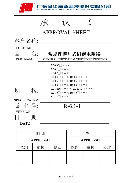
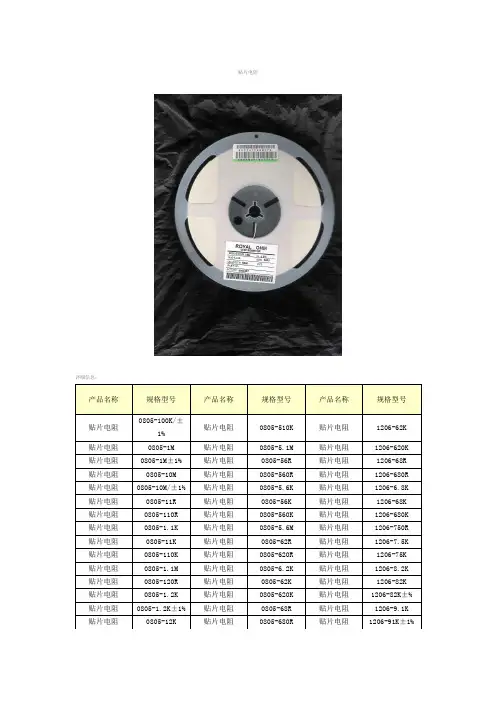
承认书APPROV AL SHEET客户名称:CUSTOMER品名:常规厚膜片式固定电阻器PARTNAME规格版本号VERSION日期DATE制造客户APPROV AL APPROV AL 拟制审核确认检验审核批准序号No目录TABLE OF CONTENTS1.0 概述Summary2.0 结构及尺寸Structure And Dimensions3.0 型号规格表示办法How To Order4.0 电气性能Performance Specification5.0 可靠性Reliability Data6.0 包装Package7.0 环保情况说明Environmental Protection Statement8.0 推荐使用的焊接曲线Recommended soldering profile9.0 使用注意事项Precautions For UseRC/RS□□□□1.0概述Summary片式电阻器主要生产的型号包括01005、0201、0402、0603、0805、1206、1210、2010、2512。
其特点是:The dimension type for chip resistor including01005、 0201、0402、0603、0805、1206、1210、2010、2512, and the features are as below:*体积小、重量轻miniature and light weight*电性能稳定,可靠性高 stable electrical capability and high reliability *机械强度高、高频特性优越superior mechanical and frequency*装配成本低,并与自动贴装设备匹配low assembly cost, suit for automatic SMT *适应再流焊与波峰焊suit for re-flow and wave flow soldering .*符合ROHS指令要求Compliant with ROHS Directive*符合无卤素要求Compliant with halogen free requirement*禁止使用SS-00259中规定的1级环境管理物质*SONY指定原材料只能从绿色伙伴认定供应商处采购产品广泛应用于计算机、通讯、工业自动化、航天航空、军事、数字电视、数字音响及消费类电子等领域。
电子器件选型指导书目录1101电阻器 (2)1102电容器 (4)1103电感器 (10)1104晶体晶振 (14)1105二极管 (17)1106三极管 (22)可编程器件 (25)1101电阻器金属膜电阻器1.推荐厂家2.选型原则(1)不论那种电阻器,都不能选用边缘极限规格;(2)对于金膜电阻器,1W以下功率优选金属膜电阻,1W及1W以上功率优选金属氧化膜电阻;(3)金属膜电阻器就是在陶瓷骨架表面,经真空高温或烧渗工艺蒸发沉积一层金属膜或合金膜。
由于其电阻体是金属或合金材料,又是在高真空条件下制备的,因而电阻器性能优良。
(4)金属膜电阻器的优点是:精度高、稳定性好、噪声低、电压系数小、体积小、高频特性好,且允许工作环境温度范围大(-55~+125℃)、温度系数低、耐热性好。
常常用作精密和高稳定性的电阻器。
(5)对于金属膜电阻器,优先选择1/4W及1/2W 功率的金属膜电阻器,当对功率、安装空间等无要求时,优选1/4W。
(6)对于金属膜电阻器,1W以下功率的优选±1%精度。
(7)对于金属膜电阻器,±1%精度的电阻器优选E96系列。
(8)对于金属膜电阻器,±5%精度的电阻器优选E24系列。
(9)对于金属膜电阻器,±0.1%精度的高精度电阻器优选E192系列。
(10)对于金属膜电阻器,电阻工作的平均功率必须小于其额定功率值的60%。
金属氧化膜电阻器1.推荐厂家2.选型原则(1)金属氧化膜电阻器的电阻体是沉积在绝缘基体表面上的一层金属氧化物薄膜(在玻璃、瓷器等材料上,通过高温以化学反应形式生成以二氧化锡为主体的金属氧化层)。
由于氧化膜膜层比较厚,因而金属氧化膜电阻器的优点是:耐磨、耐腐蚀、化学性能稳定、寄生电感量小。
(2)对于金属氧化膜电阻器,实际功率等级有1/6W、1/4W、1/2W、1W、2W、3W、5W 等。
(3)对于金属氧化膜电阻器,1W及1W 功率以上的为优选金属氧化膜电阻器。
1本文档为高品质电阻参数资料,选型手册,请需要的工程师及感兴趣的朋友参阅! 强烈推荐: A 贴片高精密电阻 B 插件高精密电阻 C 低温漂电阻 D 无感电阻 E 电流采样电阻 F 超低阻值电阻 G 合金取样电阻 H 超大电流采样电阻 I 压敏电阻 J 耐冲击电阻 K 耐高压电阻 L 特殊功能电阻,非标电阻等 M 功率电感 N 高频电感 更多资料及样品要求,请随时联系捷比信!Thick Film Chip Resistor-CR Series■ConstructionLD1WT3 4 5 6 9 87 1D221 Alumina Substrate 2 Bottom Electrode (Ag) 3 Top Electrode (Ag-Pd)4 Edge Electrode (NiCr) 5 Barrier Layer (Ni) 6 External Electrode (Sn)7 Resistor Layer (RuO2/Ag) 8 Primary Overcoat (Glass) 9 Secondary Overcoat (Epoxy) Unit: mm■Features-Small size and light weight -Highly reliable multilayer electrode construction -Compatible with all soldering process■DimensionsType Size (Inch) L W T D1 D2Weight (g) (1000pcs) 0.150 0.620 2.042 4.368 8.947 15.959 24.241 39.448CR-01 0201 0.60±0.03 0.30±0.03 0.23±0.03 0.15±0.05 0.15±0.05■Applications-Telecommunication Equipments -Radio and Tape Recorders, TV Tuners -Video Cameras, Watches, Pocket Calculators -Automotive Industry -Computers, Instruments -Medical and Military EquipmentCR-02 0402 1.00±0.05 0.50±0.05 0.35±0.05 0.20±0.10 0.20±0.10 CR-03 0603 1.60±0.10 0.80±0.10 0.45±0.10 0.30±0.20 0.30±0.20 CR-05 0805 2.00±0.10 1.25±0.10 0.50±0.10 0.35±0.20 0.40±0.20 CR-06 1206 3.10±0.10 1.55±0.10 0.55±0.10 0.50±0.25 0.50±0.20 CR-10 1210 3.20±0.20 2.60±0.15 0.55±0.10 0.50±0.25 0.50±0.20 CR-0A 2010 5.00±0.20 2.50±0.15 0.55±0.10 0.60±0.25 0.50±0.20 CR-12 2512 6.35±0.20 3.20±0.15 0.55±0.10 0.60±0.25 0.50±0.20■Part NumberingCRProduct Type 03 Dimensions F Resistance Tolerance 01: 0201 02: 0402 03: 0603 05: 0805 06: 1206 10: 1210 0A: 2010 12: 2512 B: ±0.1% C: ±0.25% D: ±0.5% F: ±1% J: ±5% L Function Code L: Standard & High Precision E: TC50 P: High Power H: Ultra High Power 7 Packaging Code 0: 7” Reel 15Kpcs 4: 7” Reel 4Kpcs 6: 7” Reel 10Kpcs 7: 7” Reel 5Kpcs 9: 10” Reel 8Kpcs A: 10” Reel 10Kpcs B: 10” Reel 20Kpcs C: 13” Reel 40Kpcs D: 13” Reel 20Kpcs F: Bulk - - - 1R2: 1.2Ω - - - 3K3: 3.3KΩ - - - 10K: 10KΩ - - 100K: 100KΩ“-“ to fill up 6 spaces- - -10R Resistance■Derating Curve100Power ratio (% )80 60 40 20 0 0 20 40 60 80 100CR-01CR-02 CR-03 CR-05 CR-06 CR-10 CR-0A CR-12120140160Ambient Temperature ( ℃ )■Standard Electrical SpecificationsItem Type CR-01 (0201) Jumper Power Rating at 70°C Jumper Rated Current 1/20W 1A Operating Temp. Range Max. Operating Voltage 25V Max. Overload Voltage 50V Resistance Range ±1% 1Ω - 10MΩ 0Ω (<50mΩ) 1Ω - 9.76Ω 10Ω - 1MΩ 1.02MΩ - 20MΩ 20.5MΩ - 100MΩ 0Ω (<50mΩ) 1Ω - 9.76Ω 10Ω - 1MΩ 1.02MΩ - 20MΩ 20.5MΩ - 100MΩ 0Ω (<50mΩ) 1Ω - 9.76Ω 10Ω - 1MΩ 1.02MΩ - 20MΩ 20.5MΩ - 100MΩ 0Ω (<50mΩ) 1Ω - 9.76Ω 10Ω - 1MΩ 1.02MΩ - 20MΩ 20.5MΩ - 39MΩ 0Ω (<50mΩ) 1Ω - 9.76Ω 10Ω - 1MΩ 1.02MΩ - 20MΩ 20.5MΩ - 100MΩ 0Ω (<50mΩ) 1Ω - 9.76Ω 10Ω - 1MΩ 1.02MΩ - 20MΩ 20.5MΩ - 100MΩ 0Ω (<50mΩ) ±5% ±200 ±200 ±100 ±200 ±400 ±200 ±100 ±200 ±400 ±200 ±100 ±200 ±400 ±200 ±100 ±200 ±400 ±200 ±100 ±200 ±400 ±200 ±100 ±200 ±400 TCR (PPM/°C)-55 ~ +125°CCR-02 (0402)1/16W-55 ~ +155°C50V100VJumper CR-03 (0603) Jumper CR-05 (0805) CR-06 (1206) Jumper CR-10 (1210) Jumper CR-0A (2010) Jumper CR-12 (2512) Jumper1A 1/10W 1A 1/8W 1/4W 2A 1/3W 2.5A 3/4W 3.5A 1W 4A -55 ~ +155°C 200V 400V 150V 300V-55 ~ +155°C75V150V-55 ~ +155°C200V400V-55 ~ +155°C200V400V-55 ~ +155°C250V500V■High Precision Electrical SpecificationsItem Type CR-02 (0402) CR-03 (0603) CR-05 (0805) CR-06 (1206) CR-10 (1210) CR-0A (2010) CR-12 (2512) Power Rating at 70°C 1/16W 1/10W 1/8W 1/4W 1/3W 3/4W 1W -55 ~ +155°C Operating Temp. Range Max. Operating Voltage 50V 75V 150V 200V 200V 200V 250V Max. Overload Voltage 100V 150V 300V 400V 400V 400V 500V Resistance Range ±0.1% ±0.25% ±0.5% TCR (PPM/°C) ±100 ±200 ±100 ±200 ±100 ±200 ±100 ±200 ±100 ±200 ±100 ±200 ±100 ±20010Ω - 1MΩ 1.02M - 10MΩ 10Ω - 1MΩ 1.02M - 10MΩ 10Ω - 1MΩ 1.02M - 10MΩ 10Ω - 1MΩ 1.02M - 10MΩ 10Ω - 1MΩ 1.02M - 10MΩ 10Ω - 1MΩ 1.02M - 10MΩ 10Ω - 1MΩ 1.02M - 10MΩ■TC50 Electrical SpecificationsItem Type CR-02 (0402) CR-03 (0603) CR-05 (0805) CR-06 (1206) CR-10 (1210) CR-0A (2010) CR-12 (2512) Power Rating at 70°C 1/16W 1/10W 1/8W 1/4W 1/3W 3/4W 1W -55 ~ +155°C Operating Temp. Range Max. Operating Voltage 50V 75V 150V 200V 200V 200V 250V Max. Overload Voltage 100V 150V 300V 400V 400V 400V 500V 10Ω 1MΩ 10Ω - 10MΩ ±50 Resistance Range ±0.1% ±0.25% ±0.5% ±1% TCR (PPM/°C)100Ω - 1MΩ■High Power & Ultra High Power Rating Electrical SpecificationsItem Type CR-02 (0402) CR-03 (0603) CR-05 (0805) CR-06 (1206) CR-10 (1210) CR-0A (2010) CR-12 (2512) *: Ultra High Power Operating Voltage=√(P*R) or Max. operating voltage listed above, whichever is lower. Overload Voltage=2.5*√(P*R) or Max. overload voltage listed above, whichever is lower. 1/3 1/2 Power Rating at 70°C 1/10W 1/8W 1/4W *1/2W *3/4W 1W 2W -55 ~ +155°C Operating Temp. Range Max. Operating Voltage 50V 50V 150V 200V 200V 200V 250V Max. Overload Voltage 100V 100V 300V 400V 400V 400V 500V 1Ω - 9.76Ω 10Ω - 1MΩ 1.02MΩ - 10MΩ ±200 ±100 ±200 Resistance Range ±1% ±5% TCR (PPM/°C)■Environmental CharacteristicsRequirement Item Temperature Coefficient of Resistance (T.C.R.) Short Time Overload ±1% and Below As Spec. ±5% Test Method Jumper -55°C~+125°C, 25°C is the reference temperature ±(2.0%+0.05Ω) <50mΩ RCWV*2.5 or Max. overload voltage for 5 seconds, 2 seconds for high power series Max. overload voltage for 1 minute 70±2°C, Max. working voltage for 1000 hrs with 1.5 hrs “ON” and 0.5 hrs “OFF” 40±2°C, 90~95% R.H. Max. working voltage for 1000 hrs with 1.5 hrs “ON” and 0.5 hrs “OFF” at +125/+155°C for 1000 hrs Bending once for 5 seconds 2010, 2512 sizes: 2mm 245±5°C for 3 seconds Other sizes: 3mm±(1.0%+0.05Ω)Insulation Resistance≥10GEndurance±(2.0%+0.10Ω)±(3.0%+0.10Ω)<100mΩDamp Heat with Load±(2.0%+0.10Ω)±(3.0%+0.10Ω)<100mΩDry Heat±(1.0%+0.05Ω)±(1.5%+0.10Ω)<50mΩBending Strength±(1.0%+0.05Ω)±(1.0%+0.05Ω)<50mΩSolderability95% min. coverageResistance to Soldering Heat±(0.5%+0.05Ω)±(1.0%+0.05Ω)<50mΩ260±5°C for 10 secondsVoltage ProofNo breakdown or flashover Individual leaching area ≦5% Total leaching area ≦ 10% ±(0.5%+0.05Ω) ±(1.0%+0.05Ω) <50mΩ1.42 times RCWV (RMS) for 1 minuteLeaching260±5°C for 30 secondsRapid Change of Temperature-55°C to +125/+155°C, 5 cyclesReference Standards: IEC 60115-1, 60068-2-58; JIS-C 5201-1 Storage Temperature: 25±3°C; Humidity < 80%RH■PackagingReel Specifications & Packaging Quantity Type CR-01 CR-01 CR-02 CR-03 CR-05 CR-06 CR-10 Packaging Quantity Paper 15K 10K Paper 20K 40K 5K Paper 10K 20K 12mm 10 inch 250±1.0 62±0.5 13.0±0.5 12.5±0.5 16.5±0.5 13 inch 7 inch 330±1.0 178.5±1.5 100±0.5 13.0±0.2 60+1/-0Unit: mm ΦA 178.5±1.5 178.5±1.5 ΦB 60 60+1/-0Tape Width 8mmReel Diameter 7 inch 7 inchΦC 13.0±0.2 13.0±0.2W 9.0±0.5 9.0±0.5T 12.5±0.5 12.5±0.5+1/-08mm10 inch254±1.0100±0.5 13.0±0.29.5±0.513.5±0.59.5±0.513.5±0.54K CR-0A Embossed CR-12 8K Paper Tape Specifications13.0±0.5 13.0±0.5 15.5±0.5Bottom TapeTop Tape Aψ D0 E F B WPaper TapeTResistorP1P2P0Direction of unreelingUnit: mm Type CR-01 CR-02 CR-03 CR-05 CR-06 CR-10 A 0.38±0.05 0.65±0.10 1.10±0.10 1.60±0.10 1.90±0.10 2.80±0.10 B 0.68±0.05 1.15±0.10 1.90±0.10 2.40±0.20 3.50±0.20 3.50±0.20 W 8.0±0.20 8.0±0.20 8.0±0.20 8.0±0.20 8.0±0.20 8.0±0.20 E 1.75±0.10 1.75±0.10 1.75±0.10 1.75±0.10 1.75±0.10 1.75±0.10 F 3.50±0.05 3.50±0.05 3.50±0.05 3.50±0.05 3.50±0.05 3.50±0.05 P0 4.00±0.10 4.00±0.10 4.00±0.10 4.00±0.10 4.00±0.10 4.00±0.10 P1 2.00±0.05 2.00±0.05 4.00±0.05 4.00±0.05 4.00±0.05 4.00±0.05 P2 ΦD0 T 0.42±0.20 0.45±0.10 0.70±0.10 0.85±0.10 0.85±0.10 0.85±0.10 2.00±0.05 1.50+0.1,-0 2.00±0.05 1.50+0.1,-0 2.00±0.05 1.50+0.1,-0 2.00±0.05 1.50+0.1,-0 2.00±0.05 1.50+0.1,-0 2.00±0.05 1.50+0.1,-0Embossed Plastic Tape Specifications Top Tape ψ D0 A B E F WTEmbossed TapeψD11.5+0.25,-0Resistor P1 P2 P0 Direction of unreeling Unit: mm T 1.2 1.2+0 +0Type CR-0A CR-12A 2.8±0.20 3.5±0.20B 5.5±0.20 6.7±0.20W 12.0±0.30 12.0±0.30E 1.75±0.10 1.75±0.10F 5.5±0.05 5.5±0.05P0 4.00±0.10 4.00±0.10P1 4.00±0.10 4.00±0.10P2 2.00±0.05 2.00±0.05ΦD0 1.50+0.1, -0 1.50+0.1, -0■Recommend Land PatternType CR-01 CR-02 CR-03 CR-05 CR-06 CR-10 CR-0A CR-12 A 0.30 0.50 0.90 1.20 2.00 2.00 3.80 3.80 B 0.25 0.45 0.60 0.70 0.90 0.90 0.90 1.60Unit: mm C 0.30 0.60 0.90 1.30 1.60 2.80 2.80 3.50CBA。