《集成电路工艺原理》试题第4章
- 格式:doc
- 大小:36.00 KB
- 文档页数:3

《集成电路工艺原理》课程考试试题- 学年第学期班级时量: 100分钟,总分 100 分,考试形式:开卷一、填空题(共12分,共6题,每题2分)1、集成度是指每个上的。
2、摩尔定律:IC 的集成度将翻一番。
年发明硅基集成电路。
3、在硅的热氧化中,有种氧化方式,氧化温度通常在以上。
4、不同晶向的硅片,它的化学、电学和机械性质,这会影响。
5、RIE的意思是,BPSG的意思是。
6、LOCOS的意思是,LDD的意思是。
二、简答题(共56分)1、影响二氧化硅热生长的因素有哪些?(8分)2、为什么要进行离子注入的退火?(8分)3、请简要回答光刻的8个基本步骤。
(8分)4、请回答刻蚀的概念及刻蚀的工艺目的。
(8分)5、请简要描述化学气相沉积CVD的概念,并写出LPCVD Si3N4的化学反应式及沉积温度(注:使用二氯二氢硅SiH2Cl2和氨气NH3沉积)。
(8分)6、请描述溅射过程(6个基本步骤)(8分)7、在“现代先进的0.18μm CMOS集成电路工艺技术”中,轻掺杂漏和侧墙的工艺目的是什么?画图示意轻掺杂漏、侧墙、源漏注入的形成。
(8分)三、计算题(共14分)1、已知某台分步重复光刻机的紫外光源的波长为365nm、其光学系统的数值孔径为0.71,试计算该设备光刻图像连续保持清晰的范围。
(7分)2、已知某台离子注入机的束斑为2.5cm2、束流为2.5mA、注入时间为1.6ms,试计算硼离子(B+)注入剂量。
(注:电子电荷q = 1.6×10⁻¹⁹库仑)(7分)四、画图题(共18分)在“早期基本的3.0μm CMOS集成电路工艺技术”中,有7大工艺步骤:1)双阱工艺;2)LOCOS隔离工艺;3)多晶硅栅结构工艺;4)源/漏(S/D)注入工艺;5)金属互连的形成;6)制作压点及合金;7)参数测试。
请写出其中的双阱工艺和LOCOS隔离工艺的具体工艺流程,并画出双阱工艺和LOCOS隔离工艺所对应的器件制作剖面图及其对应的版图(注意:版图要标出亮区或暗区;剖面图要标出各区名称)。

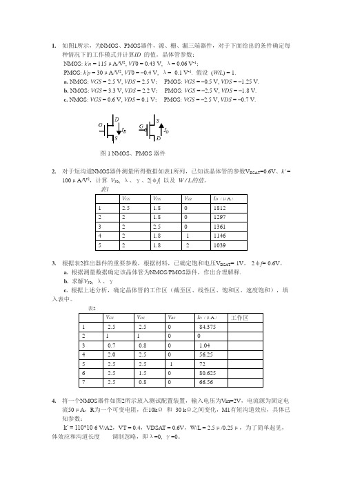
1.如图1所示,为NMOS、PMOS器件,源、栅、漏三端器件,对于下面给出的条件确定每种情况下的工作模式并计算ID 的值。
晶体管参数:NMOS: k'n = 115μA/V2, VT0 = 0.43 V, λ= 0.06 V-1;PMOS: k'p = 30μA/V2, VT0 = –0.4 V, λ= -0.1 V-1. 假设(W/L) = 1.a. NMOS: VGS = 2.5 V, VDS = 2.5 V;PMOS: VGS = –0.5 V, VDS = –1.25 V.b. NMOS: VGS = 3.3 V, VDS = 2.2 V;PMOS: VGS = –2.5 V, VDS = –1.8 V.c. NMOS: VGS = 0.6 V, VDS = 0.1 V;PMOS: VGS = –2.5 V, VDS = –0.7 V.图1 NMOS、PMOS器件2.对于短沟道NMOS器件测量所得数据如表1所列,已知该晶体管的参数V DSAT=0.6V、k' =100μA/V2,计算V T0, λ、γ、2|φf| 以及W / L的值。
表1V GS V DS V SB I D(μA)1 2.5 1.8 0 18122 2 1.8 0 12973 2 2.5 0 13614 2 1.8 -1 11465 2 1.8 -2 10393.根据表2推出器件的重要参数,根据材料,已确定饱和电压V DSAT=-1V,-2φf=-0.6V。
a. 根据测量数据确定该晶体管为NMOS/PMOS器件,作出合理解释.b. 求解V T0, λ、γc. 根据上述分析,确定晶体管的工作区(截至区、线性区、饱和区、速度饱和),填入表中。
表2V GS V DS V BS I D(μA)工作区1 -2.5 -2.5 0 -84.3752 1 1 0 03 -0.7 -0.8 0 -1.044 -2.0 -2.5 0 -56.255 -2.5 -2.5 -1 -726 -2.5 -1.5 0 -80.6257 -2.5 -0.8 0 -66.564.将一个NMOS器件如图2所示放入测试配置装置,输入电压为Vin=2V,电流源为固定电流50μA,R为一个可变电阻,在10kΩ和30 kΩ之间变化,M1有短沟道效应,具体已知参数:k’ = 110*10-6 V/A2,VT = 0.4,VDSAT = 0.6V,W/L = 2.5μ/0.25μ,为了简单起见,体效应和沟道长度调制忽略,即λ=0, γ=0。


1Chapter 4 Problem SetChapter 4Problems1.[M, None, 4.x] Figure 0.1 shows a clock-distribution network. Each segment of the clock net-work (between the nodes) is 5 mm long, 3 μm wide, and is implemented in polysilicon. Ateach of the terminal nodes (such as R ) resides a load capacitance of 100 fF.a.Determine the average current of the clock driver, given a voltage swing on the clock linesof 5 V and a maximum delay of 5 nsec between clock source and destination node R . Forthis part, you may ignore the resistance and inductance of the networkb.Unfortunately the resistance of the polysilicon cannot be ignored. Assume that eachstraight segment of the network can be modeled as a Π-network. Draw the equivalent cir-cuit and annotate the values of resistors and capacitors.c.Determine the dominant time-constant of the clock response at node R .2.[C, SPICE, 4.x] You are designing a clock distribution network in which it is critical to mini-mize skew between local clocks (CLK 1, CLK 2, and CLK 3). You have extracted the RC net-work of F igure 0.2, which models the routing parasitics of your clock line. Initially, you notice that the path to CLK 3 is shorter than to CLK 1 or CLK 2. In order to compensate for this imbalance, you insert a transmission gate in the path of CLK 3 to eliminate the skew.a.Write expressions for the time-constants associated with nodes CLK 1,CLK 2 and CLK 3.Assume the transmission gate can be modeled as a resistance R 3.b.If R 1 = R 2 = R 4 = R 5 = R and C 1 = C 2 = C 3 = C 4 = C 5 = C , what value of R 3 is required to balance the delays to CLK 1, CLK 2, and CLK 3?c.For R =750Ω and C =200fF, what (W /L )’s are required in the transmission gate to elimi-nate skew? Determine the value of the propagation delay.d.Simulate the network using SPICE, and compare the obtained results with the manually obtained numbers.3.[M, None, 4.x]Consider a CMOS inverter followed by a wire of length L . Assume that in thereference design, inverter and wire contribute equally to the total propagation delay t pref . Youmay assume that the transistors are velocity-saturated. The wire is scaled in line with the idealwire scaling model . Assume initially that the wire is a local wire .a.Determine the new (total) propagation delay as a a function of t p ref , assuming that technol-ogy and supply voltage scale with a factor 2. Consider only first-order effects.b.Perform the same analysis, assuming now that the wire scales a global wire , and the wire length scales inversely proportional to the technology.Figure 0.1Clock-distribution network.SR2Chapter 4 Problem Setc.Repeat b, but assume now that the wire is scaled along the constant resistance model. You may ignore the effect of the fringing capacitance.d.Repeat b, but assume that the new technology uses a better wiring material that reduces the resistivity by half, and a dielectric with a 25% smaller permittivity.e.Discuss the energy dissipation of part a. as a function of the energy dissipation of the orig-inal design E ref .f.Determine for each of the statements below if it is true, false, or undefined, and explain in one line your answer. - When driving a small fan-out, increasing the driver transistor sizes raises the short-circuit power dissipation. - Reducing the supply voltage, while keeping the threshold voltage constant decreases the short-circuit power dissipation.- Moving to Copper wires on a chip will enable us to build faster adders.- Making a wire wider helps to reduce its RC delay.- Going to dielectrics with a lower permittivity will make RC wire delay more impor-tant.4.[M, None, 4.x] A two-stage buffer is used to drive a metal wire of 1 cm. The first inverter is of minimum size with an input capacitance Ci=10 fF and an internal propagation delay t p0=50 ps and load dependent delay of 5ps/fF. The width of the metal wire is 3.6 μm. The sheet resis-tance of the metal is 0.08 Ω/, the capacitance value is 0.03 fF/μm 2and the fringing field capacitance is 0.04fF/μm.a.What is the propagation delay of the metal wire?pute the optimal size of the second inverter. What is the minimum delay through the buffer?c.If the input to the first inverter has 25% chance of making a 0-to-1 transition, and the whole chip is running at 20MHz with a 2.5 supply voltage, then what’s the power con-sumed by the metal wire?5.[M, None, 4.x]To connect a processor to an external memory an off -chip connection is neces-sary. The copper wire on the board is 15 cm long and acts as a transmission line with a charac-teristic impedance of 100Ω.(See F igure 0.3). The memory input pins present a very highimpedance which can be considered infinite. The bus driver is a CMOS inverter consisting ofvery large devices: (50/0.25) for the NMOS and (150/0.25) for the PMOS, where all sizes areClock CLK 1CLK 2CLK 3R 1R 2R 5R 4R 3Model as:Figure 0.2RC clock-distribution network.driver C 1C 3C 4C 5C 2Digital Integrated Circuits - 2nd Ed3 in μm. The minimum size device, (0.25/0.25) for NMOS and (0.75/0.25) for PMOS, has theon resistance 35 kΩ.a.Determine the time it takes for a change in the signal to propagate from source to destina-tion (time of flight). The wire inductance per unit length equals 75*10-8 H/m.b.Determine how long it will take the output signal to stay within 10% of its final value. Youcan model the driver as a voltage source with the driving device acting as a series resis-tance. Assume a supply and step voltage of 2.5V. Hint: draw the lattice diagram for thetransmission line.c.Resize the dimensions of the driver to minimize the total delay.L=15cmMemoryZ=100ΩFigure 0.3The driver, the connecting copper wire and thememory block being accessed.6.[M, None, 4.x] A two stage buffer is used to drive a metal wire of 1 cm. The first inverter is aminimum size with an input capacitance C i=10 fF and a propagation delay t p0=175 ps whenloaded with an identical gate. The width of the metal wire is 3.6 μm. The sheet resistance ofthe metal is 0.08 Ω/, the capacitance value is 0.03 fF/μm2 and the fringing field capacitanceis 0.04 fF/μm.a.What is the propagation delay of the metal wire?pute the optimal size of the second inverter. What is the minimum delay through thebuffer?7.[M, None, 4.x] For the RC tree given in Figure 0.4 calculate the Elmore delay from node A tonode B using the values for the resistors and capacitors given in the below in Table 0.1.Figure 0.4RC tree for calculating the delay4Chapter 4 Problem SetTable 0.1Values of the components in the RC tree of Figure 0.4Resistor Value(Ω)Capacitor Value(fF)R10.25C1250R20.25C2750R30.50C3250R4100C4250R50.25C51000R6 1.00C6250R70.75C7500R81000C82508.[M, SPICE, 4.x] In this problem the various wire models and their respective accuracies willbe studied.pute the 0%-50% delay of a 500um x 0.5um wire with resistance of 0.08 Ω/,witharea capacitance of 30aF/um2, and fringing capacitance of 40aF/um. Assume the driverhas a 100Ω resistance and negligible output capacitance.•Using a lumped model for the wire.•Using a PI model for the wire, and the Elmore equations to find tau. (see Chapter 4, figure4.26).•Using the distributed RC line equations from Chapter 4, section 4.4.4.pare your results in part a. using spice (be sure to include the source resistance). Foreach simulation, measure the 0%-50% time for the output•First, simulate a step input to a lumped R-C circuit.•Next, simulate a step input to your wire as a PI model.•Unfortunately, our version of SPICE does not support the distributed RC model as described in your book (Chapter 4, section 4.5.1). Instead, simulate a step input to yourwire using a PI3 distributed RC model.9.[M, None, 4.x] A standard CMOS inverter drives an aluminum wire on the first metal layer.Assume Rn=4kΩ, Rp=6kΩ. Also, assume that the output capacitance of the inverter is negli-gible in comparison with the wire capacitance. The wire is .5um wide, and the resistivity is0.08 Ω/..a.What is the "critical length" of the wire?b.What is the equivalent capacitance of a wire of this length? (For your capacitance calcula-tions, use Table 4.2 of your book , assume there’s field oxide underneath and nothingabove the aluminum wire)Digital Integrated Circuits - 2nd Ed510.[M, None, 4.x] A 10cm long lossless transmission line on a PC board (relative dielectric con-stant = 9, relative permeability = 1) with characteristic impedance of 50Ω is driven by a 2.5Vpulse coming from a source with 150Ω resistance.a.If the load resistance is infinite, determine the time it takes for a change at the source toreach the load (time of flight).Now a 200Ω load is attached at the end of the transmission line.b.What is the voltage at the load at t = 3ns?c.Draw lattice diagram and sketch the voltage at the load as a function of time. Determinehow long does it take for the output to be within 1 percent of its final value.11.[C, SPICE, 4.x] Assume V DD =1.5V . Also, use short-channel transistor models forhand analy-sis.a.The Figure 0.5 shows an output driver feeding a 0.2 pF effective fan-out of CMOS gates through a transmission line. Size the two transistors of the driver to optimize the delay.Sketch waveforms of V S and V L , assuming a square wave input. Label critical voltages and times.b.Size down the transistors by m times (m is to be treated as a parameter). Derive a first order expression for the time it takes for V L to settle down within 10% of its final voltage pare the obtained result with the case where no inductance is associated with the wire.Please draw the waveforms of V L for both cases, and comment.e the transistors as in part a). Suppose C L is changed to 20pF. Sketch waveforms of V S and V L , assuming a square wave input. Label critical voltages and instants.d.Assume now that the transmission line is lossy. Perform Hspice simulation for three cases:R=100 Ω/cm; R=2.5 Ω/cm; R=0.5 Ω/cm. Get the waveforms of V S , V L and the middle point of the line. Discuss the results.12.[M, None, 4.x] Consider an isolated 2mm long and 1μm wide M1(Metal1)wire over a silicon substrate driven by an inverter that has zero resistance and parasitic output capccitance. How will the wire delay change for the following cases? Explain your reasoning in each case.a.If the wire width is doubled.b.If the wire length is halved.c.If the wire thickness is doubled.d.If thickness of the oxide between the M1 and the substrate is doubled.13.[E, None, 4.x] In an ideal scaling model, where all dimensions and voltages scale with a fac-tor of S >1 :L=350nH/m 10cm C=150pF/m inV DDV DD V S V LC L =0.2pF Figure 0.5Transmission line between two inverters6Chapter 4 Problem Seta.How does the delay of an inverter scale?b.If a chip is scaled from one technology to another where all wire dimensions,including thevertical one and spacing, scale with a factor of S, how does the wire delayscale? How doesthe overall operating frequency of a chip scale?c.Repeat b) for the case where everything scales, except the vertical dimension of wires (itstays constant).。

1Chapter 4 Problem SetChapter 4Problems1.[M, None, 4.x] Figure 0.1 shows a clock-distribution network. Each segment of the clock net-work (between the nodes) is 5 mm long, 3 µm wide, and is implemented in polysilicon. Ateach of the terminal nodes (such as R ) resides a load capacitance of 100 fF.a.Determine the average current of the clock driver, given a voltage swing on the clock linesof 5 V and a maximum delay of 5 nsec between clock source and destination node R . Forthis part, you may ignore the resistance and inductance of the networkb.Unfortunately the resistance of the polysilicon cannot be ignored. Assume that eachstraight segment of the network can be modeled as a Π-network. Draw the equivalent cir-cuit and annotate the values of resistors and capacitors.c.Determine the dominant time-constant of the clock response at node R .2.[C, SPICE, 4.x] You are designing a clock distribution network in which it is critical to mini-mize skew between local clocks (CLK 1, CLK 2, and CLK 3). You have extracted the RC net-work of Figure 0.2, which models the routing parasitics of your clock line. Initially, you notice that the path to CLK 3 is shorter than to CLK 1 or CLK 2. In order to compensate for this imbalance, you insert a transmission gate in the path of CLK 3 to eliminate the skew.a.Write expressions for the time-constants associated with nodes CLK 1, CLK 2 and CLK 3.Assume the transmission gate can be modeled as a resistance R 3.b.If R 1 = R 2 = R 4 = R 5 = R and C 1 = C 2 = C 3 = C 4 = C 5 = C , what value of R 3 is required to balance the delays to CLK 1, CLK 2, and CLK 3?c.For R = 750Ω and C = 200fF, what (W /L )’s are required in the transmission gate to elimi-nate skew? Determine the value of the propagation delay.d.Simulate the network using SPICE, and compare the obtained results with the manually obtained numbers.3.[M, None, 4.x]Consider a CMOS inverter followed by a wire of length L . Assume that in thereference design, inverter and wire contribute equally to the total propagation delay t pref . Youmay assume that the transistors are velocity-saturated. The wire is scaled in line with the idealwire scaling model . Assume initially that the wire is a local wire .a.Determine the new (total) propagation delay as a a function of t p ref , assuming that technol-ogy and supply voltage scale with a factor 2. Consider only first-order effects.b.Perform the same analysis, assuming now that the wire scales a global wire , and the wire length scales inversely proportional to the technology.Figure 0.1Clock-distribution network.SR2Chapter 4 Problem Setc.Repeat b, but assume now that the wire is scaled along the constant resistance model. You may ignore the effect of the fringing capacitance.d.Repeat b, but assume that the new technology uses a better wiring material that reduces the resistivity by half, and a dielectric with a 25% smaller permittivity.e.Discuss the energy dissipation of part a. as a function of the energy dissipation of the orig-inal design E ref .f.Determine for each of the statements below if it is true, false, or undefined, and explain in one line your answer. - When driving a small fan-out, increasing the driver transistor sizes raises the short-circuit power dissipation. - Reducing the supply voltage, while keeping the threshold voltage constant decreases the short-circuit power dissipation.- Moving to Copper wires on a chip will enable us to build faster adders.- Making a wire wider helps to reduce its RC delay.- Going to dielectrics with a lower permittivity will make RC wire delay more impor-tant.4.[M, None, 4.x] A two-stage buffer is used to drive a metal wire of 1 cm. The first inverter is of minimum size with an input capacitance Ci=10 fF and an internal propagation delay t p0=50 ps and load dependent delay of 5ps/fF. The width of the metal wire is 3.6 µm. The sheet resis-tance of the metal is 0.08 Ω/, the capacitance value is 0.03 fF/µm 2 and the fringing field capacitance is 0.04fF/µm.a.What is the propagation delay of the metal wire?pute the optimal size of the second inverter. What is the minimum delay through the buffer?c.If the input to the first inverter has 25% chance of making a 0-to-1 transition, and the whole chip is running at 20MHz with a 2.5 supply voltage, then what’s the power con-sumed by the metal wire?5.[M, None, 4.x]To connect a processor to an external memory an off -chip connection is neces-sary. The copper wire on the board is 15 cm long and acts as a transmission line with a charac-teristic impedance of 100Ω.(See Figure 0.3). The memory input pins present a very highimpedance which can be considered infinite. The bus driver is a CMOS inverter consisting ofvery large devices: (50/0.25) for the NMOS and (150/0.25) for the PMOS, where all sizes areClock CLK 1CLK 2CLK 3R 1R 2R 5R 4R 3Model as:Figure 0.2RC clock-distribution network.driver C 1C 3C 4C 5C 2Digital Integrated Circuits - 2nd Ed3 in µm. The minimum size device, (0.25/0.25) for NMOS and (0.75/0.25) for PMOS, has theon resistance 35 kΩ.a.Determine the time it takes for a change in the signal to propagate from source to destina-tion (time of flight). The wire inductance per unit length equals 75*10-8 H/m.b.Determine how long it will take the output signal to stay within 10% of its final value. Youcan model the driver as a voltage source with the driving device acting as a series resis-tance. Assume a supply and step voltage of 2.5V. Hint: draw the lattice diagram for thetransmission line.c.Resize the dimensions of the driver to minimize the total delay.L=15cmMemoryZ=100ΩFigure 0.3The driver, the connecting copper wire and thememory block being accessed.6.[M, None, 4.x] A two stage buffer is used to drive a metal wire of 1 cm. The first inverter is aminimum size with an input capacitance C i=10 fF and a propagation delay t p0=175 ps whenloaded with an identical gate. The width of the metal wire is 3.6 µm. The sheet resistance ofthe metal is 0.08 Ω/, the capacitance value is 0.03 fF/µm2 and the fringing field capacitanceis 0.04 fF/µm.a.What is the propagation delay of the metal wire?pute the optimal size of the second inverter. What is the minimum delay through thebuffer?7.[M, None, 4.x] For the RC tree given in Figure 0.4 calculate the Elmore delay from node A tonode B using the values for the resistors and capacitors given in the below in Table 0.1.Figure 0.4RC tree for calculating the delay4Chapter 4 Problem SetTable 0.1Values of the components in the RC tree of Figure 0.4Resistor Value(Ω)Capacitor Value(fF)R10.25C1250R20.25C2750R30.50C3250R4100C4250R50.25C51000R6 1.00C6250R70.75C7500R81000C82508.[M, SPICE, 4.x] In this problem the various wire models and their respective accuracies willbe studied.pute the 0%-50% delay of a 500um x 0.5um wire with resistance of 0.08 Ω/,witharea capacitance of 30aF/um2, and fringing capacitance of 40aF/um. Assume the driverhas a 100Ω resistance and negligible output capacitance.•Using a lumped model for the wire.•Using a PI model for the wire, and the Elmore equations to find tau. (see Chapter 4, figure4.26).•Using the distributed RC line equations from Chapter 4, section 4.4.4.pare your results in part a. using spice (be sure to include the source resistance). Foreach simulation, measure the 0%-50% time for the output•First, simulate a step input to a lumped R-C circuit.•Next, simulate a step input to your wire as a PI model.•Unfortunately, our version of SPICE does not support the distributed RC model as described in your book (Chapter 4, section 4.5.1). Instead, simulate a step input to yourwire using a PI3 distributed RC model.9.[M, None, 4.x] A standard CMOS inverter drives an aluminum wire on the first metal layer.Assume Rn=4kΩ, Rp=6kΩ. Also, assume that the output capacitance of the inverter is negli-gible in comparison with the wire capacitance. The wire is .5um wide, and the resistivity is0.08 Ω/..a.What is the "critical length" of the wire?b.What is the equivalent capacitance of a wire of this length? (For your capacitance calcula-tions, use Table 4.2 of your book , assume there’s field oxide underneath and nothingabove the aluminum wire)Digital Integrated Circuits - 2nd Ed510.[M, None, 4.x] A 10cm long lossless transmission line on a PC board (relative dielectric con-stant = 9, relative permeability = 1) with characteristic impedance of 50Ω is driven by a 2.5Vpulse coming from a source with 150Ω resistance.a.If the load resistance is infinite, determine the time it takes for a change at the source toreach the load (time of flight).Now a 200Ω load is attached at the end of the transmission line.b.What is the voltage at the load at t = 3ns?c.Draw lattice diagram and sketch the voltage at the load as a function of time. Determinehow long does it take for the output to be within 1 percent of its final value.11.[C, SPICE, 4.x] Assume V DD =1.5V . Also, use short-channel transistor models forhand analy-sis.a.The Figure 0.5 shows an output driver feeding a 0.2 pF effective fan-out of CMOS gates through a transmission line. Size the two transistors of the driver to optimize the delay.Sketch waveforms of V S and V L , assuming a square wave input. Label critical voltages and times.b.Size down the transistors by m times (m is to be treated as a parameter). Derive a first order expression for the time it takes for V L to settle down within 10% of its final voltage pare the obtained result with the case where no inductance is associated with the wire.Please draw the waveforms of V L for both cases, and comment.e the transistors as in part a). Suppose C L is changed to 20pF. Sketch waveforms of V S and V L , assuming a square wave input. Label critical voltages and instants.d.Assume now that the transmission line is lossy. Perform Hspice simulation for three cases:R=100 Ω/cm; R=2.5 Ω/cm; R=0.5 Ω/cm. Get the waveforms of V S , V L and the middle point of the line. Discuss the results.12.[M, None, 4.x] Consider an isolated 2mm long and 1µm wide M1(Metal1)wire over a silicon substrate driven by an inverter that has zero resistance and parasitic output capccitance. How will the wire delay change for the following cases? Explain your reasoning in each case.a.If the wire width is doubled.b.If the wire length is halved.c.If the wire thickness is doubled.d.If thickness of the oxide between the M1 and the substrate is doubled.13.[E, None, 4.x] In an ideal scaling model, where all dimensions and voltages scale with a fac-tor of S >1 :L=350nH/m 10cm C=150pF/m inV DDV DD V S V LC L =0.2pF Figure 0.5Transmission line between two inverters6Chapter 4 Problem Seta.How does the delay of an inverter scale?b.If a chip is scaled from one technology to another where all wire dimensions,including thevertical one and spacing, scale with a factor of S, how does the wire delayscale? How doesthe overall operating frequency of a chip scale?c.Repeat b) for the case where everything scales, except the vertical dimension of wires (itstays constant).。
1Chapter 4 Problem SetChapter 4Problems1.[M, None, 4.x] Figure 0.1 shows a clock-distribution network. Each segment of the clock net-work (between the nodes) is 5 mm long, 3 μm wide, and is implemented in polysilicon. Ateach of the terminal nodes (such as R ) resides a load capacitance of 100 fF.a.Determine the average current of the clock driver, given a voltage swing on the clock linesof 5 V and a maximum delay of 5 nsec between clock source and destination node R . Forthis part, you may ignore the resistance and inductance of the networkb.Unfortunately the resistance of the polysilicon cannot be ignored. Assume that eachstraight segment of the network can be modeled as a Π-network. Draw the equivalent cir-cuit and annotate the values of resistors and capacitors.c.Determine the dominant time-constant of the clock response at node R .2.[C, SPICE, 4.x] You are designing a clock distribution network in which it is critical to mini-mize skew between local clocks (CLK 1, CLK 2, and CLK 3). You have extracted the RC net-work of F igure 0.2, which models the routing parasitics of your clock line. Initially, you notice that the path to CLK 3 is shorter than to CLK 1 or CLK 2. In order to compensate for this imbalance, you insert a transmission gate in the path of CLK 3 to eliminate the skew.a.Write expressions for the time-constants associated with nodes CLK 1,CLK 2 and CLK 3.Assume the transmission gate can be modeled as a resistance R 3.b.If R 1 = R 2 = R 4 = R 5 = R and C 1 = C 2 = C 3 = C 4 = C 5 = C , what value of R 3 is required to balance the delays to CLK 1, CLK 2, and CLK 3?c.For R =750Ω and C =200fF, what (W /L )’s are required in the transmission gate to elimi-nate skew? Determine the value of the propagation delay.d.Simulate the network using SPICE, and compare the obtained results with the manually obtained numbers.3.[M, None, 4.x]Consider a CMOS inverter followed by a wire of length L . Assume that in thereference design, inverter and wire contribute equally to the total propagation delay t pref . Youmay assume that the transistors are velocity-saturated. The wire is scaled in line with the idealwire scaling model . Assume initially that the wire is a local wire .a.Determine the new (total) propagation delay as a a function of t p ref , assuming that technol-ogy and supply voltage scale with a factor 2. Consider only first-order effects.b.Perform the same analysis, assuming now that the wire scales a global wire , and the wire length scales inversely proportional to the technology.Figure 0.1Clock-distribution network.SR2Chapter 4 Problem Setc.Repeat b, but assume now that the wire is scaled along the constant resistance model. You may ignore the effect of the fringing capacitance.d.Repeat b, but assume that the new technology uses a better wiring material that reduces the resistivity by half, and a dielectric with a 25% smaller permittivity.e.Discuss the energy dissipation of part a. as a function of the energy dissipation of the orig-inal design E ref .f.Determine for each of the statements below if it is true, false, or undefined, and explain in one line your answer. - When driving a small fan-out, increasing the driver transistor sizes raises the short-circuit power dissipation. - Reducing the supply voltage, while keeping the threshold voltage constant decreases the short-circuit power dissipation.- Moving to Copper wires on a chip will enable us to build faster adders.- Making a wire wider helps to reduce its RC delay.- Going to dielectrics with a lower permittivity will make RC wire delay more impor-tant.4.[M, None, 4.x] A two-stage buffer is used to drive a metal wire of 1 cm. The first inverter is of minimum size with an input capacitance Ci=10 fF and an internal propagation delay t p0=50 ps and load dependent delay of 5ps/fF. The width of the metal wire is 3.6 μm. The sheet resis-tance of the metal is 0.08 Ω/, the capacitance value is 0.03 fF/μm 2and the fringing field capacitance is 0.04fF/μm.a.What is the propagation delay of the metal wire?pute the optimal size of the second inverter. What is the minimum delay through the buffer?c.If the input to the first inverter has 25% chance of making a 0-to-1 transition, and the whole chip is running at 20MHz with a 2.5 supply voltage, then what’s the power con-sumed by the metal wire?5.[M, None, 4.x]To connect a processor to an external memory an off -chip connection is neces-sary. The copper wire on the board is 15 cm long and acts as a transmission line with a charac-teristic impedance of 100Ω.(See F igure 0.3). The memory input pins present a very highimpedance which can be considered infinite. The bus driver is a CMOS inverter consisting ofvery large devices: (50/0.25) for the NMOS and (150/0.25) for the PMOS, where all sizes areClock CLK 1CLK 2CLK 3R 1R 2R 5R 4R 3Model as:Figure 0.2RC clock-distribution network.driver C 1C 3C 4C 5C 2Digital Integrated Circuits - 2nd Ed3 in μm. The minimum size device, (0.25/0.25) for NMOS and (0.75/0.25) for PMOS, has theon resistance 35 kΩ.a.Determine the time it takes for a change in the signal to propagate from source to destina-tion (time of flight). The wire inductance per unit length equals 75*10-8 H/m.b.Determine how long it will take the output signal to stay within 10% of its final value. Youcan model the driver as a voltage source with the driving device acting as a series resis-tance. Assume a supply and step voltage of 2.5V. Hint: draw the lattice diagram for thetransmission line.c.Resize the dimensions of the driver to minimize the total delay.L=15cmMemoryZ=100ΩFigure 0.3The driver, the connecting copper wire and thememory block being accessed.6.[M, None, 4.x] A two stage buffer is used to drive a metal wire of 1 cm. The first inverter is aminimum size with an input capacitance C i=10 fF and a propagation delay t p0=175 ps whenloaded with an identical gate. The width of the metal wire is 3.6 μm. The sheet resistance ofthe metal is 0.08 Ω/, the capacitance value is 0.03 fF/μm2 and the fringing field capacitanceis 0.04 fF/μm.a.What is the propagation delay of the metal wire?pute the optimal size of the second inverter. What is the minimum delay through thebuffer?7.[M, None, 4.x] For the RC tree given in Figure 0.4 calculate the Elmore delay from node A tonode B using the values for the resistors and capacitors given in the below in Table 0.1.Figure 0.4RC tree for calculating the delay4Chapter 4 Problem SetTable 0.1Values of the components in the RC tree of Figure 0.4Resistor Value(Ω)Capacitor Value(fF)R10.25C1250R20.25C2750R30.50C3250R4100C4250R50.25C51000R6 1.00C6250R70.75C7500R81000C82508.[M, SPICE, 4.x] In this problem the various wire models and their respective accuracies willbe studied.pute the 0%-50% delay of a 500um x 0.5um wire with resistance of 0.08 Ω/,witharea capacitance of 30aF/um2, and fringing capacitance of 40aF/um. Assume the driverhas a 100Ω resistance and negligible output capacitance.•Using a lumped model for the wire.•Using a PI model for the wire, and the Elmore equations to find tau. (see Chapter 4, figure4.26).•Using the distributed RC line equations from Chapter 4, section 4.4.4.pare your results in part a. using spice (be sure to include the source resistance). Foreach simulation, measure the 0%-50% time for the output•First, simulate a step input to a lumped R-C circuit.•Next, simulate a step input to your wire as a PI model.•Unfortunately, our version of SPICE does not support the distributed RC model as described in your book (Chapter 4, section 4.5.1). Instead, simulate a step input to yourwire using a PI3 distributed RC model.9.[M, None, 4.x] A standard CMOS inverter drives an aluminum wire on the first metal layer.Assume Rn=4kΩ, Rp=6kΩ. Also, assume that the output capacitance of the inverter is negli-gible in comparison with the wire capacitance. The wire is .5um wide, and the resistivity is0.08 Ω/..a.What is the "critical length" of the wire?b.What is the equivalent capacitance of a wire of this length? (For your capacitance calcula-tions, use Table 4.2 of your book , assume there’s field oxide underneath and nothingabove the aluminum wire)Digital Integrated Circuits - 2nd Ed510.[M, None, 4.x] A 10cm long lossless transmission line on a PC board (relative dielectric con-stant = 9, relative permeability = 1) with characteristic impedance of 50Ω is driven by a 2.5Vpulse coming from a source with 150Ω resistance.a.If the load resistance is infinite, determine the time it takes for a change at the source toreach the load (time of flight).Now a 200Ω load is attached at the end of the transmission line.b.What is the voltage at the load at t = 3ns?c.Draw lattice diagram and sketch the voltage at the load as a function of time. Determinehow long does it take for the output to be within 1 percent of its final value.11.[C, SPICE, 4.x] Assume V DD =1.5V . Also, use short-channel transistor models forhand analy-sis.a.The Figure 0.5 shows an output driver feeding a 0.2 pF effective fan-out of CMOS gates through a transmission line. Size the two transistors of the driver to optimize the delay.Sketch waveforms of V S and V L , assuming a square wave input. Label critical voltages and times.b.Size down the transistors by m times (m is to be treated as a parameter). Derive a first order expression for the time it takes for V L to settle down within 10% of its final voltage pare the obtained result with the case where no inductance is associated with the wire.Please draw the waveforms of V L for both cases, and comment.e the transistors as in part a). Suppose C L is changed to 20pF. Sketch waveforms of V S and V L , assuming a square wave input. Label critical voltages and instants.d.Assume now that the transmission line is lossy. Perform Hspice simulation for three cases:R=100 Ω/cm; R=2.5 Ω/cm; R=0.5 Ω/cm. Get the waveforms of V S , V L and the middle point of the line. Discuss the results.12.[M, None, 4.x] Consider an isolated 2mm long and 1μm wide M1(Metal1)wire over a silicon substrate driven by an inverter that has zero resistance and parasitic output capccitance. How will the wire delay change for the following cases? Explain your reasoning in each case.a.If the wire width is doubled.b.If the wire length is halved.c.If the wire thickness is doubled.d.If thickness of the oxide between the M1 and the substrate is doubled.13.[E, None, 4.x] In an ideal scaling model, where all dimensions and voltages scale with a fac-tor of S >1 :L=350nH/m 10cm C=150pF/m inV DDV DD V S V LC L =0.2pF Figure 0.5Transmission line between two inverters6Chapter 4 Problem Seta.How does the delay of an inverter scale?b.If a chip is scaled from one technology to another where all wire dimensions,including thevertical one and spacing, scale with a factor of S, how does the wire delayscale? How doesthe overall operating frequency of a chip scale?c.Repeat b) for the case where everything scales, except the vertical dimension of wires (itstays constant).。
集成电路工艺原理相关试题一、选择题1.集成电路工艺的发展历经了以下哪几个阶段? A. 自由扩散阶段、光刻成型阶段、微影速度阶段 B. 预扩散台阶、纳米光刻阶段、电子束曝光阶段C. 扩散二极管阶段、光刻馏分阶段、微影速度阶段 D. 电子束曝光阶段、分子束曝光阶段、纳米光刻阶段2.下列哪种是集成电路工艺中常用的掩模技术? A. 仰视照相法 B. 紫外光刻法 C. 照相法 D. 磁控溅射法3.集成电路工艺中的光刻成像的基本过程包括哪些步骤? A. 刻蚀、扫描、照射 B. 曝光、显影、清洗 C. 感光、曝光、显影 D. 感光、曝光、刻蚀4.下列哪种材料不适合用于集成电路的制作? A. 硅 B. 铝 C. 铜 D. 锡5.集成电路工艺中的扩散过程是指什么? A. 材料中杂质的扩散 B. 将电路图案转移到硅片上的象限 C. 利用高温使材料的原子迁移 D. 利用光照使光刻胶产生化学反应二、填空题1.集成电路工艺中,常用的曝光技术是将光照射在待制作电路上,通过光刻胶对光进行控制,达到光刻胶的显影,从而得到所需的图形。
2.集成电路工艺中,光刻胶的主要组成是聚合物和光敏剂。
3.集成电路中的 MOSFET 制作过程中,常用的氧化物层材料是SiO2。
4.集成电路中,扩散过程会引入适量的杂质,以改变材料的导电性能。
5.集成电路工艺中,常用的金属导线材料是铝。
三、简答题1.请简要介绍集成电路工艺中的光刻成像过程。
光刻成像是集成电路工艺中常用的掩模技术之一,其基本过程包括:–感光:在待制作电路表面涂上一层光刻胶,将器件图形的反转图案转移到光刻胶上。
–曝光:将待制作电路与光刻胶一起暴露在紫外光下,通过光刻胶中的光敏剂吸收光能而发生化学反应,使得光刻胶的物理和化学性质发生变化,在胶层上形成图形。
–显影:通过将光刻胶浸泡在显影液中,溶解未暴露于光的部分,得到所需的图形。
2.集成电路中的扩散过程是指什么?请简要描述扩散过程的基本原理。
电子与通信技术:集成电路工艺原理考试资料(题库版)1、问答题简述引线框架材料?正确答案:引线框架作为集成电路的芯片载体,是一种借助于键合材料(金丝、铝丝、铜丝)实现芯片内部电路引出端与外引线的电气连接,形成电气回路的关(江南博哥)键结构件,它起到了和外部导线连接的桥梁作用。
引线框架材料的要求为:热匹配,良好的机械性能,导电、导热性能好,使用过程无相变,材料中杂质少,低价,加工特性和二次性能好。
2、问答题简述MCM的概念、分类与特性?正确答案:概念:将多块半导体裸芯片组装在一块布线基板上的一种封装。
分类:MCM-L是采用片状多层基板的MCM、MCM-C是采用多层陶瓷基板的MCM、MCM-D是采用薄膜技术的MCM。
特性:尺寸小、技术集成度高、数据速度和信号质量高、可靠性高、成本低、PCB板设计简化、提高圆片利用率、降低投资风险。
可大幅度提高电路连线密度,增加封装效率;可完成轻、薄、短、小的封装设计;封装的可靠性提升。
3、问答题矩形片式电阻由哪几部分组成?各部分的主要作用是什么?正确答案:基板:基板要具有良好的电绝G8P-1A4PDC12缘性、导热性和机械强度高等特征。
一般基板的材科多采用高纯度的(96%)AL203陶瓷。
其工艺要求表面平整、划线准确,以确保电阻、电极浆料印制到位。
电极:片式电阻器一般都采用三层电极结构,最内层的是内层电极,它是连接电阻体位于中间层的是中间电极,它是镀镍(Ni)层,也被称为阻挡层,其主要作用是提高电阻器在焊接时的耐热性,避免造成内层电极被溶蚀。
位于最外层的是外层电极,它也被称为可焊层,该层除了使电极具有良好的可焊性外,还可以起到延长电极保存期的作用。
通常,外层电极采用锡一铅(S。
-PB.合金电镀而成。
电阻膜:电阻膜是采用具有一定电阻率的电阻浆料印制在陶瓷基板上,然后再经过烧结而成的厚膜电阻。
保护层:保护层位于电阻膜的外部,主要起保护作用。
它通常可以细分为封包玻璃保护膜、玻璃釉涂层和标志玻璃层。
集成电路工艺原理相关试题(doc 17页)一、填空题(30分=1分*30)10题/章晶圆制备1.用来做芯片的高纯硅被称为(半导体级硅),英文简称(GSG ),有时也被称为(电子级硅)。
2.单晶硅生长常用(CZ法)和(区熔法)两种生长方式,生长后的单晶硅被称为(硅锭)。
3.晶圆的英文是(wafer ),其常用的材料是(硅)和(锗)。
4.晶圆制备的九个工艺步骤分别是(单晶生长)、整型、(切片)、磨片倒角、刻蚀、(抛光)、清洗、检查和包装。
5.从半导体制造来讲,晶圆中用的最广的晶体平面的密勒符号是(100 )、(110 )和(111 )。
6.CZ直拉法生长单晶硅是把(融化了的半导体级硅液体)变为(有正确晶向的)并且(被掺杂成p型或n型)的固体硅锭。
7.CZ直拉法的目的是(实现均匀掺杂的同时并且复制仔晶的结构,得到合适的硅锭直径并且限制杂质引入到硅中)。
影响CZ直拉法的两个主要参数是(拉伸速率)和(晶体旋转速率)。
8.晶圆制备中的整型处理包括(去掉两端)、(径向研磨)和(硅片定位边和定位槽)。
9.制备半导体级硅的过程:1(制备工业硅);2(生长硅单晶);3(提纯)。
氧化10.二氧化硅按结构可分为()和()或()。
11.热氧化工艺的基本设备有三种:(卧式炉)、(立式炉)和(快速热处理炉)。
12.根据氧化剂的不同,热氧化可分为(干氧氧化)、(湿氧氧化)和(水汽氧化)。
13.用于热工艺的立式炉的主要控制系统分为五部分:(工艺腔)、(硅片传输系统)、气体分配系统、尾气系统和(温控系统)。
14.选择性氧化常见的有(局部氧化)和(浅槽隔离),其英语缩略语分别为LOCOS和(STI )。
15.列出热氧化物在硅片制造的4种用途:(掺杂阻挡)、(表面钝化)、场氧化层和(金属层间介质)。
16.可在高温设备中进行的五种工艺分别是(氧化)、(扩散)、()、退火和合金。
17.硅片上的氧化物主要通过(热生长)和(淀积)的方法产生,由于硅片表面非常平整,使得产生的氧化物主要为层状结构,所以又称为(薄膜)。
第四章
填空题
1.注入离子在靶内的能量损失分为和两个过程。
2.使一个处于晶格位置的原子发生移位,所需要的最小能量称为。
3.当离子注入的方向与靶晶体的某个晶向平行时,会出现。
4.是表征注入离子分布分散情况的一个量。
5.横向效应与注入离子的和有关。
答案
1 核碰撞,电子碰撞
2 移位阈能
3 沟道效应
4 标准偏差
5 种类,能量
选择题
1.离子注入时,使晶体主轴方向偏离注入方向是为了避免。
B
A.横向效应
B.沟道效应
C. 热电子效应
2.注入离子的能量可分为三个区域,高能区是以占主要地位。
A
A. 电子阻止本领
B. 核阻止本领
C. 核阻止和电子阻止本领
3.注入离子的能量可分为三个区域,低能区是以占主要地位。
A
A.核阻止本领
B.电子阻止本领
C. 核阻止和电子阻止本领
4.注入离子的能量可分为三个区域,中能区是以占主要地位。
C
A.核阻止本领
B.电子阻止本领
C. 核阻止和电子阻止本领
判断题
1.相同能量注入离子,离子越轻,横向效应越显著。
( ) √
2.相同离子,能量越轻,横向效应越显著。
( ) ×
3.轻离子在注入的初始阶段,其损伤是以电子阻止为主导。
()√
4.轻离子在注入时,其损伤是以核阻止为主导。
()×
5.重离子在注入时,其损伤是以电子阻止为主导。
()×
6.重离子在注入时,其损伤是以核阻止为主导。
()√
7.等离子体中高速运动的电子与其它粒子的碰撞是维持气体放电的主要微观机制。
()√
名词解释
1.级联碰撞
2.等离子体韒层
3.RTP
4.热退火
5.沟道效应
6.横向效应
7.LSS理论
答案
1.级联碰撞:ET»Ed:位移原子(反冲原子)再与靶原子碰撞,产生级联碰撞。
2.等离子体鞘层--是电子与离子具有不同速度的一个直接后果。
即任何处于等离子体中
的物体相对于等离子体来讲都呈现出负电位,并且在物体的表面附近出现正电荷积累。
3.RTP:快速退火技术,瞬时内使硅片的某个区域加热到所需要的温度,并在较短的时
间内完成退火。
4.热退火:将注有离子的硅片在一定温度下,经过适当时间的热处理,则硅片上的损伤
可能部分或绝大部分得到消除,少数载流子的寿命以及迁移率也会不同程度的得到恢复,掺入的杂质也将得到一定比例的电激活,这样的处理过程称为热退火。
5.沟道效应:离子沿沟道前进,核阻挡作用小,因而射程比非晶靶远的多。
好处:结较
深;晶格损伤小。
不利:难于获得可重复的浓度分布,使用价值小。
6.横向效应:指注入离子在垂直入射方向的平面内的分布情况。
它直接影响了MOS晶
体管的有效沟道长度。
7.LSS理论:(Lindhard,Scharff,Schiot三人创立)①核碰撞(阻挡),注入离子与靶
原子核碰撞,将能量传给靶核,离子发生偏转,靶核产生位移。
②电子碰撞(阻挡)注入离子与靶内的自由电子和束缚电子碰撞,产生电子-空穴对。
注入离子运动方向基本不变。
8.沟道效应:离子沿沟道前进,核阻挡作用小,因而射程比非晶靶远的多。
好处:结较
深;晶格损伤小。
不利:难于获得可重复的浓度分布,使用价值小。
9.横向效应:指注入离子在垂直入射方向的平面内的分布情况。
它直接影响了MOS晶
体管的有效沟道长度。
10.LSS理论:(Lindhard,Scharff,Schiot三人创立)①核碰撞(阻挡),注入离子与靶
原子核碰撞,将能量传给靶核,离子发生偏转,靶核产生位移。
②电子碰撞(阻挡)注入离子与靶内的自由电子和束缚电子碰撞,产生电子-空穴对。
注入离子运动方向基本不变。
问答题
1.注入离子在硅衬底中产生的损伤有哪几种?
答案
答:有以下三种:
(1)在原本为完美晶体的硅中产生孤立的点缺陷或缺陷群;(2)在晶体中形成局部的非晶区域;
(3)由于注入离子引起损伤的积累而形成非晶层。