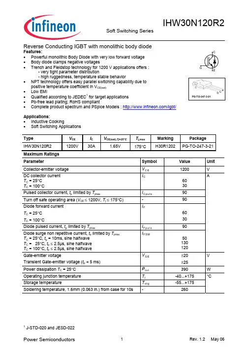
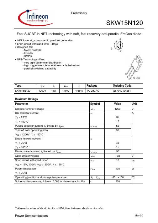
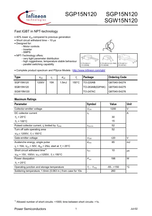
Fast S-IGBT in NPT-technology with soft, fast recovery anti-parallel EmCon diode• 40% lower E off compared to previous generation •Short circuit withstand time – 10 µs • Designed for:- Motor controls - Inverter - SMPS• NPT-Technology offers:- very tight parameter distribution- high ruggedness, temperature stable behaviour - parallel switching capabilityType V CE I C E off T j Package Ordering Code SKW15N1201200V15A1.5mJ150°CTO-247ACQ67040-S4281Maximum Ratings ParameterSymbol Value Unit Collector-emitter voltage V C E 1200V DC collector current T C = 25°C T C = 100°CI C3015Pulsed collector current, t p limited by T jmax I C p u l s 52Turn off safe operating area V CE ≤ 1200V, T j ≤ 150°C -52Diode forward current T C = 25°C T C = 100°CI F3215Diode pulsed current, t p limited by T jmax I F p u l s 50AGate-emitter voltage V G E ±20V Short circuit withstand time 1)V GE = 15V, 100V ≤ V CC ≤1200V, T j ≤ 150°Ct S C 10µs Power dissipation T C = 25°CP t o t 198W Operating junction and storage temperatureT j , T s t g -55...+150Soldering temperature, 1.6mm (0.063 in.) from case for 10s-260°CThermal Resistance Parameter Symbol Conditions Max. ValueUnit CharacteristicIGBT thermal resistance,junction – caseR t h J C 0.63Diode thermal resistance,junction – case R t h J C D 1.5Thermal resistance,junction – ambientR t h J ATO-247AC 40K/WElectrical Characteristic, at T j = 25 °C, unless otherwise specified ValueParameterSymbol Conditionsmin.typ.max.UnitStatic CharacteristicCollector-emitter breakdown voltage V (B R )C E S V G E =0V,I C =1000µA 1200--Collector-emitter saturation voltageV C E (s a t )V G E = 15V, I C =15A T j =25°C T j =150°C2.5-3.13.7 3.64.3Diode forward voltageV FV G E =0V, I F =15A T j =25°C T j =150°C- 2.01.752.5Gate-emitter threshold voltage V G E (t h )I C =600µA,V C E =V G E 345VZero gate voltage collector currentI C E SV CE =1200V,V GE =0V T j =25°C T j =150°C----200800µAGate-emitter leakage current I G E S V CE =1200V,V GE =0V --100nA Transconductance g f s V C E =20V, I C =15A 11-S Dynamic Characteristic Input capacitance C i s s -12901550Output capacitanceC o s s -155185Reverse transfer capacitance C r s s V C E =25V,V G E =0V,f =1MHz-90110pFGate chargeQ G a t e V C C =960V, I C =15A V G E =15V -130175nC Internal emitter inductancemeasured 5mm (0.197 in.) from case L E TO-247AC-13-nH Short circuit collector current1)I C (S C )V G E =15V,t S C ≤10µs 100V ≤V C C ≤1200V,T j ≤ 150°C-145-ASwitching Characteristic, Inductive Load, at T j =25 °C ValueParameterSymbolConditionsmin.typ.max.UnitIGBT Characteristic Turn-on delay time t d (o n )-1824Rise timet r -2330Turn-off delay time t d (o f f )-580750Fall time t f -2229nsTurn-on energy E o n - 1.1 1.5Turn-off energy E o f f -0.8 1.1Total switching energyE t sT j =25°C,V C C =800V,I C =15A,V G E =15V/0V,R G =33Ω,Energy losses include “tail” and diode reverse recovery.- 1.92.6mJ Anti-Parallel Diode Characteristic Diode reverse recovery timet r r t S t F---65 nsDiode reverse recovery charge Q r r -0.5µC Diode peak reverse recovery current I r r m -15A Diode peak rate of fall of reverse recovery current during t Fdi r r /dtT j =25°C,V R =800V, I F =15A,di F /dt =650A/µs-500A/µs Switching Characteristic, Inductive Load, at T j =150 °C ValueParameterSymbolConditionsmin.typ.max.UnitIGBT Characteristic Turn-on delay time t d (o n )-3846Rise timet r -3036Turn-off delay time t d (o f f )-652780Fall time t f -3137nsTurn-on energy E o n - 1.9 2.3Turn-off energy E o f f - 1.5 2.0Total switching energyE t sT j =150°C V C C =800V,I C =15A,V G E =15V/0V,R G =33ΩEnergy losses include “tail” and diode reverse recovery.- 3.44.3mJ Anti-Parallel Diode Characteristic Diode reverse recovery timet r r t S t F---200 nsDiode reverse recovery charge Q r r - 2.0µC Diode peak reverse recovery current I r r m -23A Diode peak rate of fall of reverse recovery current during t Fdi r r /dtT j =150°CV R =800V, I F =15A,di F /dt =650A/µs-140A/µsI C , C O L L E C T O R C U R R E N T10Hz100Hz 1kHz 10kHz 100kHz 0A 10A 20A 30A 40A 50A 60A 70AI C , C O L L E C T O R C U R R E N T1V 10V 100V 1000V0.1A1A10A100Af , SWITCHING FREQUENCYV CE , COLLECTOR -EMITTER VOLTAGE Figure 1. Collector current as a function of switching frequency(T j ≤ 150°C, D = 0.5, V CE = 800V,V GE = +15V/0V, R G = 33Ω)Figure 2. Safe operating area (D = 0, T C = 25°C, T j ≤ 150°C)P t o t , P O W E R D I S S I P A T I O N25°C50°C 75°C 100°C 125°C 0W 25W 50W 75W 100W 125W 150W 175W 200WI C , C O L L E C T O R C U R R E N T25°C50°C 75°C 100°C 125°C0A5A 10A 15A 20A 25A 30A35AT C , CASE TEMPERATURET C , CASE TEMPERATUREFigure 3. Power dissipation as a function of case temperature (T j ≤ 150°C)Figure 4. Collector current as a function of case temperature(V GE ≤ 15V, T j ≤ 150°C)I C , C O L L E C T O R C U R R E N T0V1V 2V 3V 4V 5V 6V 7V0A 10A20A30A40A 50AI C , C O L L E C T O R C U R R E N T0V1V 2V 3V 4V 5V 6V 7V0A 10A20A30A40A50AV CE , COLLECTOR -EMITTER VOLTAGEV CE , COLLECTOR -EMITTER VOLTAGEFigure 5. Typical output characteristics (T j = 25°C)Figure 6. Typical output characteristics (T j = 150°C)I C , C O L L E C T O R C U R R E N T3V5V 7V 9V 11V0A 10A20A30A40A50AV C E (s a t ), C O L L E C T O R -E M I T T E R S A T U R A T I O N V O L T A G E-50°C0°C 50°C 100°C 150°C0V1V2V3V4V5V6VV GE , GATE -EMITTER VOLTAGET j , JUNCTION TEMPERATUREFigure 7. Typical transfer characteristics (V CE = 20V)Figure 8. Typical collector-emittersaturation voltage as a function of junction temperature (V GE = 15V)t , S W I T C H I N G T I M E S0A10A20A30A40A10ns100ns1000nst , S W I T C H I N G T I M E S0Ω25Ω50Ω10ns100ns1000nsI C , COLLECTOR CURRENTR G , GATE RESISTORFigure 9. Typical switching times as a function of collector current(inductive load, T j = 150°C, V CE = 8600V,V GE = +15V/0V, R G = 33Ω)Figure 10. Typical switching times as a function of gate resistor(inductive load, T j = 150°C, V CE = 800V,V GE = +15V/0V, I C = 15A)t , S W I T C H I N G T I M E S-50°C0°C 50°C 100°C 150°C10ns100ns1000nsV G E (t h ), G A T E -E M I T T E R T H R E S H O L D V O L T A G E-50°C0°C 50°C 100°C150°C0V1V2V3V4V5V6VT j , JUNCTION TEMPERATURET j , JUNCTION TEMPERATUREFigure 11. Typical switching times as a function of junction temperature(inductive load, V CE = 800V, V GE = +15V/0V,I C = 15A, R G = 33Ω)Figure 12. Gate-emitter threshold voltage as a function of junction temperature (I C = 0.3mA)E , S W I T C H I N G E N E R G Y L O S S E S0A10A 20A 30A 40A 50A0mJ 2mJ 4mJ 6mJ 8mJ10mJ 12mJ14mJE , SW I T C H I N G E N E R G Y L O S S E S0Ω25Ω50Ω75Ω0mJ 1mJ2mJ3mJ4mJ5mJI C , COLLECTOR CURRENTR G , GATE RESISTORFigure 13. Typical switching energy losses as a function of collector current(inductive load, T j = 150°C, V CE = 800V,V GE = +15V/0V, R G = 33Ω)Figure 14. Typical switching energy losses as a function of gate resistor(inductive load, T j = 150°C, V CE = 800V,V GE = +15V/0V, I C = 15A)E , SW I T C H I N G E N E R G Y L O S S E S-50°C0°C 50°C 100°C 150°C0mJ 1mJ2mJ3mJ4mJZ t h J C , T R A N S I E N T T H E R M A L I M P E D A N C E1µs10µs100µs1ms 10ms 100ms 1s10-3K/W10-2K/W 10-1K/WT j , JUNCTION TEMPERATUREt p , PULSE WIDTHFigure 15. Typical switching energy losses as a function of junction temperature (inductive load, V CE = 800V, V GE = +15V/0V,I C = 15A, R G = 33Ω)Figure 16. IGBT transient thermalimpedance as a function of pulse width (D = t p / T )V G E , G A T E -E M I T T E R V O L T A G E0nC50nC100nC150nC0V 5V10V15V20VC , C A P A C I T A N C E0V10V20V30V100pF1nFQ GE , GATE CHARGEV CE , COLLECTOR -EMITTER VOLTAGE Figure 17. Typical gate charge (I C = 15A)Figure 18. Typical capacitance as a function of collector-emitter voltage (V GE = 0V, f = 1MHz)t s c , S H O R T C I R C U I T W I T H S T A N D T I M E10V 11V12V13V14V15V0µs10µs20µs30µsI C (s c ), S H O R T C I R C U I T C O L L E C T O R C U R R E N T10V12V 14V 16V18V 20V0A 50A100A150A200A250A300AV GE , GATE -EMITTER VOLTAGEV GE , GATE -EMITTER VOLTAGEFigure 19. Short circuit withstand time as a function of gate-emitter voltage (V CE = 1200V, start at T j = 25°C)Figure 20. Typical short circuit collector current as a function of gate-emitter voltage (100V ≤V CE ≤1200V, T C = 25°C, T j ≤ 150°C)t r r , R E V E R S E R E C O V E R Y T I M E200A/µs400A/µs 600A/µs 800A/µs 1000A/µs0ns50ns 100ns 150ns 200ns 250ns 300ns 350ns400nsQ r r , R E V E R S E R E C O V E R Y C H A R G E200A/µs400A/µs 600A/µs 800A/µs 1000A/µs0.0µC0.5µC1.0µC1.5µC2.0µC2.5µCdi F /dt , DIODE CURRENT SLOPEdi F /dt , DIODE CURRENT SLOPEFigure 21. Typical reverse recovery time as a function of diode current slope (V R = 800V, T j = 150°C)Figure 22. Typical reverse recovery charge as a function of diode current slope (V R = 800V, T j = 150°C)I r r , R E V E R S E R E C O V E R Y C U R R E N T200A/µs400A/µs 600A/µs 800A/µs 1000A/µs0A5A10A15A20A25A30Ad i r r /d t , D I O D E P E A K R A T E O F F A L LO F R E V E R S E R E C O V E R Y C U R R E N T200A/µs400A/µs 600A/µs 800A/µs 1000A/µs0A/µs100A/µs200A/µs300A/µs400A/µsdi F /dt , DIODE CURRENT SLOPEdi F /dt , DIODE CURRENT SLOPEFigure 23. Typical reverse recovery current as a function of diode current slope (V R = 800V, T j = 150°C)Figure 24. Typical diode peak rate of fall of reverse recovery current as a function of diode current slope (V R = 800V, T j = 150°C)I F , F O R W A R D C U R R E N T0V1V 2V 3V 4V0A 10A20A30A40A50AV F , F O R W A R D V O L T A G E0°C40°C 80°C 120°C0.0V0.5V1.0V1.5V2.0V2.5V3.0VV F , FORWARD VOLTAGET j , JUNCTION TEMPERATUREFigure 25. Typical diode forward current as a function of forward voltage Figure 26. Typical diode forward voltage as a function of junction temperatureZ t h J C D , T R A N S I E N T T H E R M A L I M P E D A N C E10µs100µs 1ms 10ms 100ms 1s10-2K/W10-1K/W100K/Wt p , PULSE WIDTHFigure 27. Diode transient thermalimpedance as a function of pulse width (D = t p / T )dimensionssymbol[mm][inch]minmax minmax A 4.78 5.280.18820.2079B 2.29 2.510.09020.0988C 1.78 2.290.07010.0902D 1.09 1.320.04290.0520E 1.73 2.060.06810.0811F 2.67 3.180.10510.1252G 0.76 max 0.0299 maxH 20.8021.160.81890.8331K 15.6516.150.61610.6358L 5.21 5.720.20510.2252M 19.8120.680.77990.8142N 3.560 4.9300.14020.1941∅P3.610.1421Q6.126.220.24090.2449TO-247ACFigure A. Definition of switching timesIr r m90% Ir r m10% Ir r mdi/dtFtr rIFi,vtQSQFtStFVRdi/dtr rQ=Q Qr r S F+t=t tr r S F+Figure C. Definition of diodesswitching characteristicsτ1τ2nτr r rFigure D. Thermal equivalentcircuitFigure B. Definition of switching lossesPublished byInfineon Technologies AG i Gr.,Bereich KommunikationSt.-Martin-Strasse 53,D-81541 München© Infineon Technologies AG 1999All Rights Reserved.Attention please!The information herein is given to describe certain components and shall not be considered as warranted characteristics. Terms of delivery and rights to technical change reserved.We hereby disclaim any and all warranties, including but not limited to warranties of non-infringement, regarding circuits, descriptions and charts stated herein.Infineon Technologies is an approved CECC manufacturer.InformationFor further information on technology, delivery terms and conditions and prices please contact your nearest Infineon Technologies Office in Germany or our Infineon Technologies Representatives worldwide (see address list).WarningsDue to technical requirements components may contain dangerous substances. For information on the types in question please contact your nearest Infineon Technologies Office.Infineon Technologies Components may only be used in life-support devices or systems with the express written approval of Infineon Technologies, if a failure of such components can reasonably be expected to cause the failure of that life-support device or system, or to affect the safety or effectiveness of that device or system. Life support devices or systems are intended to be implanted in the human body, or to support and/or maintain and sustain and/or protecthuman life. If they fail, it is reasonable to assume that the health of the user or other persons may be endangered.。