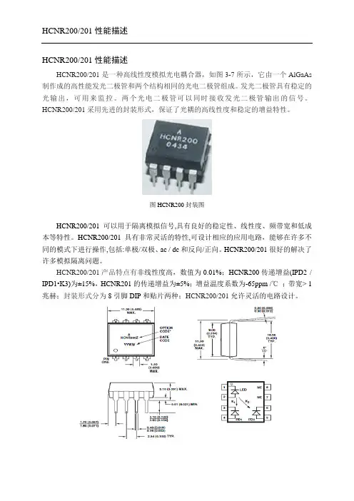
HCNR201中文资料
- 格式:pdf
- 大小:245.19 KB
- 文档页数:16
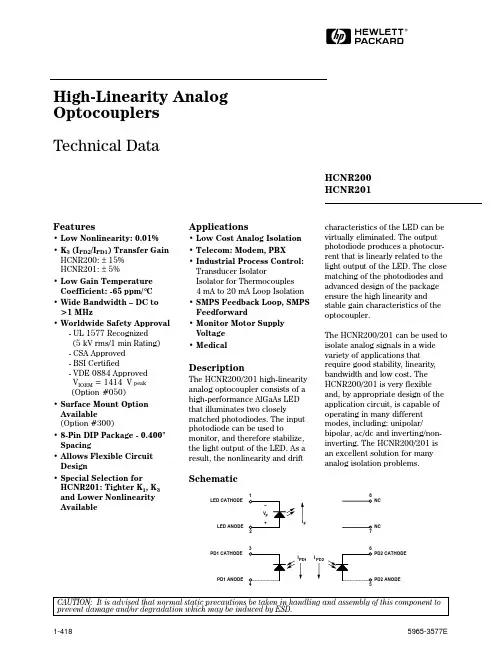
1-418HHigh-Linearity Analog Optocouplers Technical DataHCNR200HCNR201CAUTION: It is advised that normal static precautions be taken in handling and assembly of this component to prevent damage and /or degradation which may be induced by ESD.I FIPD1I PD2NCNC PD2 CATHODEPD2 ANODELED CATHODELED ANODEPD1 CATHODEPD1 ANODEFeatures• Low Nonlinearity: 0.01%• K 3 (I PD2/I PD1) Transfer Gain HCNR200: ±15%HCNR201: ±5%• Low Gain Temperature Coefficient: -65ppm/°C • Wide Bandwidth – DC to >1 MHz• Worldwide Safety Approval-UL 1577 Recognized (5 kV rms/1 min Rating)-CSA Approved -BSI Certified-VDE 0884 Approved V IORM = 1414 V peak (Option #050)• Surface Mount Option Available(Option #300)• 8-Pin DIP Package - 0.400"Spacing• Allows Flexible Circuit Design• Special Selection forHCNR201: Tighter K 1, K 3and Lower Nonlinearity AvailableApplications• Low Cost Analog Isolation • Telecom: Modem, PBX• Industrial Process Control:Transducer IsolatorIsolator for Thermocouples 4mA to 20 mA Loop Isolation • SMPS Feedback Loop, SMPS Feedforward• Monitor Motor Supply Voltage • MedicalDescriptionThe HCNR200/201 high-linearity analog optocoupler consists of a high-performance AlGaAs LED that illuminates two closelymatched photodiodes. The input photodiode can be used tomonitor, and therefore stabilize,the light output of the LED. As a result, the nonlinearity and driftcharacteristics of the LED can be virtually eliminated. The output photodiode produces a photocur-rent that is linearly related to the light output of the LED. The close matching of the photodiodes and advanced design of the package ensure the high linearity and stable gain characteristics of the optocoupler.The HCNR200/201 can be used to isolate analog signals in a wide variety of applications that require good stability, linearity,bandwidth and low cost. The HCNR200/201 is very flexible and, by appropriate design of the application circuit, is capable of operating in many different modes, including: unipolar/bipolar, ac/dc and inverting/non-inverting. The HCNR200/201 is an excellent solution for many analog isolation problems.Schematic5965-3577E1-419Ordering Information:HCNR20x0 = ±15% Transfer Gain, 0.25% Maximum Nonlinearity 1 = ±5% Transfer Gain, 0.05% Maximum NonlinearityOption yyy050 = VDE 0884 V IORM = 1414 V peak Option 300 = Gull Wing Surface Mount Lead Option 500 = Tape/Reel Package Option (1 k min.)Option data sheets available. Contact your Hewlett-Packard sales representative or authorized distributor for information.Package Outline DrawingsFigure 1.MAX."V" = OPTION 050OPTION NUMBERS 300 AND 500 NOT MARKED.1-420Gull Wing Surface Mount Option #300240TIME – MINUTEST E M P E R A T U R E – °C220200180160140120100806040200260(NOTE: USE OF NON-CHLORINE ACTIVATED FLUXES IS RECOMMENDED.)Maximum Solder Reflow Thermal ProfileRegulatory InformationThe HCNR200/201 optocoupler features a 0.400" wide, eight pin DIP package. This package was specifically designed to meet worldwide regulatory require-ments. The HCNR200/201 has been approved by the following organizations:ULRecognized under UL 1577, Component Recognition Program,FILE E55361CSAApproved under CSA Component Acceptance Notice #5, File CA 88324BSICertification according to BS415:1994;(BS EN60065:1994);BS EN60950:1992(BS7002:1992) andEN41003:1993 for Class II applicationsVDEApproved according to VDE 0884/06.92(Available Option #050only)1.78 ± 0.15 MAX.BSCDIMENSIONS IN MILLIMETERS (INCHES).LEAD COPLANARITY = 0.10 mm (0.004 INCHES).Insulation and Safety Related SpecificationsParameter Symbol Value Units ConditionsMin. External Clearance L(IO1)9.6mm Measured from input terminals to output (External Air Gap)terminals, shortest distance through air Min. External Creepage L(IO2)10.0mm Measured from input terminals to output (External Tracking Path)terminals, shortest distance path along body Min. Internal Clearance 1.0mm Through insulation distance conductor to (Internal Plastic Gap)conductor, usually the direct distancebetween the photoemitter and photodetectorinside the optocoupler cavityMin. Internal Creepage 4.0mm The shortest distance around the border (Internal Tracking Path)between two different insulating materialsmeasured between the emitter and detector Comparative Tracking Index CTI200V DIN IEC 112/VDE 0303 PART 1Isolation Group IIIa Material group (DIN VDE 0110)Option 300 – surface mount classification is Class A in accordance with CECC 00802.VDE 0884 (06.92) Insulation Characteristics (Option #050 Only)Description Symbol Characteristic Unit Installation classification per DIN VDE 0110/1.89, Table 1For rated mains voltage ≤600 V rms I-IVFor rated mains voltage ≤1000 V rms I-IIIClimatic Classification (DIN IEC 68 part 1)55/100/21Pollution Degree (DIN VDE 0110 Part 1/1.89)2Maximum Working Insulation Voltage V IORM1414V peak Input to Output Test Voltage, Method b*V PR2651V peak V PR = 1.875 x V IORM, 100% Production Test witht m = 1 sec, Partial Discharge < 5 pCInput to Output Test Voltage, Method a*V PR2121V peak V PR = 1.5 x V IORM, Type and sample test, t m = 60 sec,Partial Discharge < 5 pCHighest Allowable Overvoltage*V IOTM8000V peak (Transient Overvoltage, t ini = 10 sec)Safety-Limiting Values(Maximum values allowed in the event of a failure,also see Figure 11)Case Temperature T S150°C Current (Input Current I F, P S = 0)I S400mA Output Power P S,OUTPUT700mW Insulation Resistance at T S, V IO = 500 V R S>109Ω*Refer to the front of the Optocoupler section of the current catalog for a more detailed description of VDE 0884 and other product safety regulations.Note: Optocouplers providing safe electrical separation per VDE 0884 do so only within the safety-limiting values to which they are qualified. Protective cut-out switches must be used to ensure that the safety limits are not exceeded.1-421Absolute Maximum RatingsStorage Temperature..................................................-55°C to +125°C Operating Temperature (T A)........................................-55°C to +100°C Junction Temperature (T J)............................................................125°C Reflow Temperature Profile...See Package Outline Drawings Section Lead Solder Temperature..................................................260°C for 10s (up to seating plane)Average Input Current - I F............................................................25 mA Peak Input Current - I F.................................................................40 mA (50 ns maximum pulse width)Reverse Input Voltage - V R..............................................................2.5 V (I R = 100 µA, Pin 1-2)Input Power Dissipation.........................................60 mW @ T A = 85°C (Derate at 2.2 mW/°C for operating temperatures above 85°C) Reverse Output Photodiode Voltage................................................30 V (Pin 6-5)Reverse Input Photodiode Voltage...................................................30 V (Pin 3-4)Recommended Operating ConditionsStorage Temperature....................................................-40°C to +85°C Operating Temperature.................................................-40°C to +85°C Average Input Current - I F.......................................................1 - 20 mA Peak Input Current - I F.................................................................35 mA (50% duty cycle, 1 ms pulse width)Reverse Output Photodiode Voltage...........................................0 - 15 V (Pin 6-5)Reverse Input Photodiode Voltage..............................................0 - 15 V (Pin 3-4)1-422Electrical Specifications1-423AC Electrical SpecificationsT A = 25°C unless otherwise specified.TestParameter Symbol Device Min.Typ.Max.Units Conditions Fig.Note LED Bandwidth f -3dB9MHz I F = 10 mAApplication Circuit Bandwidth:High Speed 1.5MHz167 High Precision10kHz177 Application Circuit: IMRRHigh Speed95dB freq = 60 Hz167, 8 Package CharacteristicsT= 25°C unless otherwise specified.Notes:1. K3 is calculated from the slope of thebest fit line of I PD2 vs. I PD1 with elevenequally distributed data points from5nA to 50 µA. This is approximatelyequal to I PD2/I PD1 at I F = 10 mA.2. Special selection for tighter K1, K3 andlower Nonlinearity available.3. BEST FIT DC NONLINEARITY (NL BF) isthe maximum deviation expressed as a percentage of the full scale output of a “best fit” straight line from a graph ofI PD2 vs. I PD1 with eleven equally distrib-uted data points from 5 nA to 50µA.I PD2 error to best fit line is the deviationbelow and above the best fit line,expressed as a percentage of the fullscale output.4. ENDS FIT DC NONLINEARITY (NL EF)is the maximum deviation expressed asa percentage of full scale output of astraight line from the 5 nA to the 50 µAdata point on the graph of I PD2 vs. I PD1.5. Device considered a two-terminaldevice: Pins 1, 2, 3, and 4 shortedtogether and pins 5, 6, 7, and 8 shortedtogether.6. In accordance with UL 1577, eachoptocoupler is proof tested by applyingan insulation test voltage of ≥6000 Vrms for ≥1 second (leakage detectioncurrent limit, I I-O of 5 µA max.). Thistest is performed before the 100%production test for partial discharge(method b) shown in the VDE 0884Insulation Characteristics Table (forOption #050 only).7. Specific performance will depend oncircuit topology and components.8. IMRR is defined as the ratio of thesignal gain (with signal applied to V IN ofFigure 16) to the isolation mode gain(with V IN connected to input commonand the signal applied between theinput and output commons) at 60 Hz,expressed in dB.*The Input-Output Momentary Withstand Voltage is a dielectric voltage rating that should not be interpreted as an input-output continuous voltage rating. For the continuous voltage rating refer to the VDE 0884 Insulation Characteristics Table (if applicable), your equipment level safety specification, or HP Application Note 1074, “Optocoupler Input-Output Endurance Voltage.”1-4241-425Figure 5. NL BF vs. Temperature.Figure 2. Normalized K3 vs. Input I PD .Figure 3. K3 Drift vs. Temperature.Figure 4. I PD2 Error vs. Input I PD (See Note 4).Figure 6. NL BF Drift vs. Temperature.Figure 7. Input Photodiode CTR vs.LED Input Current.Figure 8. Typical Photodiode Leakage vs. Temperature.Figure 9. LED Input Current vs.Forward Voltage.Figure 10. LED Forward Voltage vs.Temperature.I L K – P H O T O D I O D E L E A K A G E – n AT A – TEMPERATURE – °C D E L T A K 3 – D R I F T O F K 3 T R A N S F E R G A I NT A – TEMPERATURE – °C D E L T A N L B F – D R I F T O F B E S T -F I T N L – % P T ST A – TEMPERATURE – °C N O R M A L I Z E D K 1 – I N P U T P H O T O D I O D E C T RI F – LED INPUT CURRENT – mAV F – L E D F O R W A R D V O L T A G E – VT A – TEMPERATURE – °C-25-555356595125N O R M A L I Z E D K 3 – T R A N S F E R G AI NI PD1 – INPUT PHOTODIODE CURRENT – µAI PD1 – INPUT PHOTODIODE CURRENT – µAI P D 2 E R R O R F R O M B E S T -F I T L I N E (% O F F S )N L B F – B E S T -F I T N O N -L I N E A R I T Y – %T A – TEMPERATURE – °C 1.201000.10.0001V F – FORWARD VOLTAGE – VOLTS 1.30 1.501010.010.001 1.40 1.60I F – F O R W A R D C U R R E N T – m AT A = 25°C1-426Figure 12. Basic Isolation Amplifier.FV I OUTV PD2OUTA) BASIC TOPOLOGYB) PRACTICAL CIRCUITFigure 11. Thermal Derating Curve Dependence of Safety Limiting Valuewith Case Temperature per VDE 0884.VOUTV OUTA) POSITIVE INPUTB) POSITIVE OUTPUTD) NEGATIVE OUTPUTFigure 13. Unipolar Circuit Topologies.T S – CASE TEMPERATURE – °C1-427Figure 15. Loop-Powered 4-20 mA Current Loop Circuits.Figure 14. Bipolar Circuit Topologies.OUTV OUTA) SINGLE OPTOCOUPLERB) DUAL OPTOCOUPLERVOUT+I OUTA) RECEIVERB) TRANSMITTERV -I OUT1-428Figure 18. Bipolar Isolation Amplifier.Figure 16. High-Speed Low-Cost Analog Isolator.VOUTINPUT BNCV +15 V OUTPUT BNCFigure 17. Precision Analog Isolation Amplifier.MAGV IN1-429MAGV INSIGNFigure 20. SPICE Model Listing.Figure 19. Magnitude/Sign Isolation Amplifier..SUBCKT HCNR200Theory of Operation Figure 1 illustrates how the HCNR200/201 high-linearity optocoupler is configured. The basic optocoupler consists of an LED and two photodiodes. The LED and one of the photodiodes (PD1) is on the input leadframe and the other photodiode (PD2) is on the output leadframe. The package of the optocoupler is constructed so that each photo-diode receives approximately the same amount of light from the LED.An external feedback amplifier can be used with PD1 to monitor the light output of the LED and automatically adjust the LED current to compensate for any non-linearities or changes in light output of the LED. The feedback amplifier acts to stabilize and linearize the light output of the LED. The output photodiode then converts the stable, linear light output of the LED into a current, which can then be converted back into a voltage by another amplifier.Figure 12a illustrates the basic circuit topology for implementing a simple isolation amplifier using the HCNR200/201 optocoupler. Besides the optocoupler, two external op-amps and two resistors are required. This simple circuit is actually a bit too simple to function properly in an actual circuit, but it is quite useful for explaining how the basic isolation amplifier circuit works (a few more components and a circuit change are required to make a practical circuit, like the one shown in Figure 12b).The operation of the basic circuit may not be immediately obvious just from inspecting Figure 12a,particularly the input part of thecircuit. Stated briefly, amplifierA1 adjusts the LED current (I F),and therefore the current in PD1(I PD1), to maintain its “+” inputterminal at 0 V. For example,increasing the input voltage wouldtend to increase the voltage of the“+” input terminal of A1 above 0V. A1 amplifies that increase,causing I F to increase, as well asI PD1. Because of the way that PD1is connected, I PD1 will pull the “+”terminal of the op-amp backtoward ground. A1 will continueto increase I F until its “+”terminal is back at 0 V. Assumingthat A1 is a perfect op-amp, nocurrent flows into the inputs ofA1; therefore, all of the currentflowing through R1 will flowthrough PD1. Since the “+” inputof A1 is at 0 V, the currentthrough R1, and therefore I PD1 aswell, is equal to V IN/R1.Essentially, amplifier A1 adjusts I Fso thatI PD1 = V IN/R1.Notice that I PD1 depends ONLY onthe input voltage and the value ofR1 and is independent of the lightoutput characteristics of the LED.As the light output of the LEDchanges with temperature, ampli-fier A1 adjusts I F to compensateand maintain a constant currentin PD1. Also notice that I PD1 isexactly proportional to V IN, givinga very linear relationship betweenthe input voltage and thephotodiode current.The relationship between the inputoptical power and the outputcurrent of a photodiode is verylinear. Therefore, by stabilizingand linearizing I PD1, the lightoutput of the LED is alsostabilized and linearized. Andsince light from the LED falls onboth of the photodiodes, I PD2 willbe stabilized as well.The physical construction of thepackage determines the relativeamounts of light that fall on thetwo photodiodes and, therefore,the ratio of the photodiodecurrents. This results in verystable operation over time andtemperature. The photodiodecurrent ratio can be expressed asa constant, K, whereK = I PD2/I PD1.Amplifier A2 and resistor R2 forma trans-resistance amplifier thatconverts I PD2 back into a voltage,V OUT, whereV OUT = I PD2*R2.Combining the above threeequations yields an overallexpression relating the outputvoltage to the input voltage,V OUT/V IN = K*(R2/R1).Therefore the relationshipbetween V IN and V OUT is constant,linear, and independent of thelight output characteristics of theLED. The gain of the basic isola-tion amplifier circuit can beadjusted simply by adjusting theratio of R2 to R1. The parameterK (called K3 in the electricalspecifications) can be thought ofas the gain of the optocoupler andis specified in the data sheet.Remember, the circuit inFigure12a is simplified in orderto explain the basic circuit opera-tion. A practical circuit, more likeFigure12b, will require a fewadditional components to stabilizethe input part of the circuit, tolimit the LED current, or to1-4301-431second circuit requires two optocouplers, separate gain adjustments for the positive and negative portions of the signal,and can exhibit crossover distor-tion near zero volts. The correct circuit to choose for an applica-tion would depend on therequirements of that particular application. As with the basic isolation amplifier circuit inFigure 12a, the circuits in Figure 14 are simplified and would require a few additional compo-nents to function properly. Two example circuits that operate with bipolar input signals arediscussed in the next section.As a final example of circuit design flexibility, the simplified schematics in Figure 15 illustrate how to implement 4-20 mA analog current-loop transmitter and receiver circuits using the HCNR200/201 optocoupler. An important feature of these circuits is that the loop side of the circuit is powered entirely by the loop current, eliminating the need for an isolated power supply.The input and output circuits in Figure 15a are the same as the negative input and positive output circuits shown in Figures 13c and 13b, except for the addition of R3and zener diode D1 on the input side of the circuit. D1 regulates the supply voltage for the input amplifier, while R3 forms a current divider with R1 to scale the loop current down from 20mA to an appropriate level for the input circuit (<50 µA).As in the simpler circuits, the input amplifier adjusts the LED current so that both of its input terminals are at the same voltage.The loop current is then dividedoptimize circuit performance.Example application circuits will be discussed later in the data sheet.Circuit Design FlexibilityCircuit design with the HCNR200/201 is very flexible because the LED and both photodiodes are accessible to the designer. This allows the designer to make perf-ormance trade-offs that would otherwise be difficult to make with commercially available isolation amplifiers (e.g., bandwidth vs.accuracy vs. cost). Analog isola-tion circuits can be designed for applications that have either unipolar (e.g., 0-10 V) or bipolar (e.g., ±10 V) signals, with positive or negative input oroutput voltages. Several simplified circuit topologies illustrating the design flexibility of the HCNR200/201 are discussed below.The circuit in Figure 12a is configured to be non-inverting with positive input and output voltages. By simply changing the polarity of one or both of the photodiodes, the LED, or the op-amp inputs, it is possible toimplement other circuit configu-rations as well. Figure 13illustrates how to change the basic circuit to accommodate both positive and negative input and output voltages. The input and output circuits can bematched to achieve any combina-tion of positive and negative voltages, allowing for both inverting and non-inverting circuits.All of the configurations described above are unipolar (single polar-ity); the circuits cannot accommo-date a signal that might swing both positive and negative. It ispossible, however, to use the HCNR200/201 optocoupler to implement a bipolar isolation amplifier. Two topologies that allow for bipolar operation are shown in Figure 14.The circuit in Figure 14a uses two current sources to offset the signal so that it appears to be unipolar to the optocoupler.Current source I OS1 provides enough offset to ensure that I PD1is always positive. The second current source, I OS2, provides an offset of opposite polarity toobtain a net circuit offset of zero.Current sources I OS1 and I OS2 can be implemented simply as resistors connected to suitable voltage sources.The circuit in Figure 14b uses two optocouplers to obtain bipolar operation. The first optocoupler handles the positive voltage excursions, while the second optocoupler handles the negative ones. The output photodiodes are connected in an antiparallel configuration so that they produce output signals of opposite polarity.The first circuit has the obvious advantage of requiring only one optocoupler; however, the offset performance of the circuit isdependent on the matching of I OS1and I OS2 and is also dependent on the gain of the optocoupler.Changes in the gain of the opto-coupler will directly affect the offset of the circuit.The offset performance of the second circuit, on the other hand,is much more stable; it is inde-pendent of optocoupler gain and has no matched current sources to worry about. However, thebetween R1 and R3. I PD1 is equal to the current in R1 and is given by the following equation:I PD1 = I LOOP*R3/(R1+R3).Combining the above equation with the equations used for Figure 12a yields an overall expression relating the output voltage to the loop current,V OUT/I LOOP = K*(R2*R3)/(R1+R3).Again, you can see that the relationship is constant, linear, and independent of the charac-teristics of the LED.The 4-20 mA transmitter circuit in Figure15b is a little different from the previous circuits, partic-ularly the output circuit. The output circuit does not directly generate an output voltage which is sensed by R2, it instead usesQ1 to generate an output current which flows through R3. This output current generates a voltage across R3, which is then sensed by R2. An analysis similar to the one above yields the following expression relating output current to input voltage:I LOOP/V IN = K*(R2+R3)/(R1*R3).The preceding circuits were pre-sented to illustrate the flexibility in designing analog isolation circuits using the HCNR200/201. The next section presents several complete schematics to illustrate practical applications of the HCNR200/201.Example Application CircuitsThe circuit shown in Figure 16 is a high-speed low-cost circuit designed for use in the feedback path of switch-mode power supplies. This application requiresgood bandwidth, low cost andstable gain, but does not requirevery high accuracy. This circuit isa good example of how a designercan trade off accuracy to achieveimprovements in bandwidth andcost. The circuit has a bandwidthof about 1.5 MHz with stable gaincharacteristics and requires fewexternal components.Although it may not appear so atfirst glance, the circuit in Figure16 is essentially the same as thecircuit in Figure 12a. Amplifier A1is comprised of Q1, Q2, R3 andR4, while amplifier A2 iscomprised of Q3, Q4, R5, R6 andR7. The circuit operates in thesame manner as well; the onlydifference is the performance ofamplifiers A1 and A2. The lowergains, higher input currents andhigher offset voltages affect theaccuracy of the circuit, but notthe way it operates. Because thebasic circuit operation has notchanged, the circuit still has goodgain stability. The use of discretetransistors instead of op-ampsallowed the design to trade offaccuracy to achieve goodbandwidth and gain stability atlow cost.To get into a little more detailabout the circuit, R1 is selected toachieve an LED current of about7-10 mA at the nominal inputoperating voltage according to thefollowing equation:I F = (V IN/R1)/K1,where K1 (i.e., I PD1/I F) of theoptocoupler is typically about0.5%. R2 is then selected toachieve the desired output voltageaccording to the equation,V OUT/V IN = R2/R1.The purpose of R4 and R6 is toimprove the dynamic response(i.e., stability) of the input andoutput circuits by lowering thelocal loop gains. R3 and R5 areselected to provide enoughcurrent to drive the bases of Q2and Q4. And R7 is selected so thatQ4 operates at about the samecollector current as Q2.The next circuit, shown inFigure17, is designed to achievethe highest possible accuracy at areasonable cost. The highaccuracy and wide dynamic rangeof the circuit is achieved by usinglow-cost precision op-amps withvery low input bias currents andoffset voltages and is limited bythe performance of the opto-coupler. The circuit is designed tooperate with input and outputvoltages from 1 mV to 10 V.The circuit operates in the sameway as the others. The only majordifferences are the two compensa-tion capacitors and additionalLED drive circuitry. In the high-speed circuit discussed above, theinput and output circuits arestabilized by reducing the localloop gains of the input and outputcircuits. Because reducing theloop gains would decrease theaccuracy of the circuit, twocompensation capacitors, C1 andC2, are instead used to improvecircuit stability. These capacitorsalso limit the bandwidth of thecircuit to about 10 kHz and canbe used to reduce the outputnoise of the circuit by reducing itsbandwidth even further.The additional LED drive circuitry(Q1 and R3 through R6) helps tomaintain the accuracy and band-width of the circuit over the entirerange of input voltages. Withoutthese components, the transcon-ductance of the LED driver would1-432decrease at low input voltages and LED currents. This would reduce the loop gain of the input circuit, reducing circuit accuracy and bandwidth. D1 prevents excessive reverse voltage from being applied to the LED when the LED turns off completely.No offset adjustment of the circuit is necessary; the gain can be adjusted to unity by simply adjusting the 50kohm poten-tiometer that is part of R2. Any OP-97 type of op-amp can be used in the circuit, such as theLT1097 from Linear Technology or the AD705 from Analog Devices, both of which offer pA bias currents, µV offset voltages and are low cost. The input terminals of the op-amps and the photodiodes are connected in the circuit using Kelvin connections to help ensure the accuracy of the circuit.The next two circuits illustrate how the HCNR200/201 can be used with bipolar input signals. The isolation amplifier inFigure18 is a practical implemen-tation of the circuit shown in Figure14b. It uses two opto-couplers, OC1 and OC2; OC1 handles the positive portions of the input signal and OC2 handles the negative portions.Diodes D1 and D2 help reduce crossover distortion by keeping both amplifiers active during both positive and negative portions of the input signal. For example, when the input signal positive, optocoupler OC1 is active while OC2 is turned off. However, the amplifier controlling OC2 is kept active by D2, allowing it to turn on OC2 more rapidly when the input signal goes negative, thereby reducing crossover distortion.Balance control R1 adjusts therelative gain for the positive andnegative portions of the inputsignal, gain control R7 adjusts theoverall gain of the isolationamplifier, and capacitors C1-C3provide compensation to stabilizethe amplifiers.The final circuit shown inFigure19 isolates a bipolaranalog signal using only oneoptocoupler and generates twooutput signals: an analog signalproportional to the magnitude ofthe input signal and a digitalsignal corresponding to the signof the input signal. This circuit isespecially useful for applicationswhere the output of the circuit isgoing to be applied to an analog-to-digital converter. The primaryadvantages of this circuit are verygood linearity and offset, withonly a single gain adjustment andno offset or balance adjustments.To achieve very high linearity forbipolar signals, the gain should beexactly the same for both positiveand negative input polarities. Thiscircuit achieves excellent linearityby using a single optocoupler anda single input resistor, whichguarantees identical gain for bothpositive and negative polarities ofthe input signal. This precisematching of gain for both polari-ties is much more difficult toobtain when separate componentsare used for the different inputpolarities, such as is the previouscircuit.The circuit in Figure19 is actuallyvery similar to the previouscircuit. As mentioned above, onlyone optocoupler is used. Becausea photodiode can conduct currentin only one direction, two diodes(D1 and D2) are used to steer theinput current to the appropriateterminal of input photodiode PD1to allow bipolar input currents.Normally the forward voltagedrops of the diodes would cause aserious linearity or accuracyproblem. However, an additionalamplifier is used to provide anappropriate offset voltage to theother amplifiers that exactlycancels the diode voltage drops tomaintain circuit accuracy.Diodes D3 and D4 perform twodifferent functions; the diodeskeep their respective amplifiersactive independent of the inputsignal polarity (as in the previouscircuit), and they also provide thefeedback signal to PD1 thatcancels the voltage drops ofdiodes D1 and D2.Either a comparator or an extraop-amp can be used to sense thepolarity of the input signal anddrive an inexpensive digitaloptocoupler, like a 6N139.It is also possible to convert thiscircuit into a fully bipolar circuit(with a bipolar output signal) byusing the output of the 6N139 todrive some CMOS switches toswitch the polarity of PD2depending on the polarity of theinput signal, obtaining a bipolaroutput voltage swing.HCNR200/201 SPICEModelFigure 20 is the net list of aSPICE macro-model for theHCNR200/201 high-linearityoptocoupler. The macro-modelaccurately reflects the primarycharacteristics of the HCNR200/201 and should facilitate thedesign and understanding ofcircuits using the HCNR200/201optocoupler.1-433。