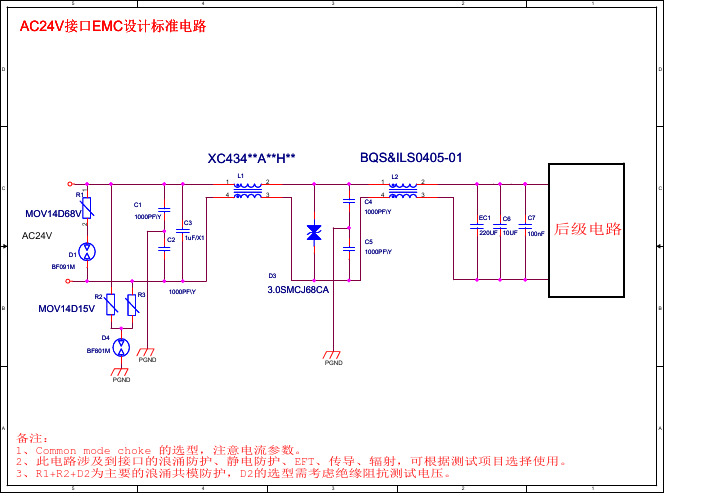
9054RDK官方原理图-860_Schematic_r300
- 格式:pdf
- 大小:256.46 KB
- 文档页数:10
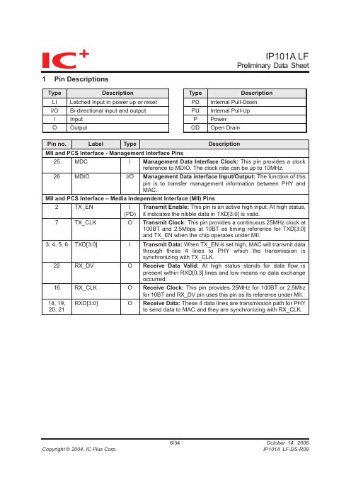
IP101A LF Preliminary Data Sheet6/34Oct ober 14, 2006Copyright © 2004, IC Plus Corp. IP101A LF-DS-R081 Pin Descriptions TypeDescription LILatched Input in power up or reset I/O Bi-directional input and output I Input O Output Type Description PD Internal Pull-Down PU Internal Pull-UpP PowerOD Open DrainPin no. LabelType Description MII and PCS Interface - Management Interface Pins25 MDC I Management Data Interface Clock: This pin provides a clockreference to MDIO. The clock rate can be up to 10MHz.26 MDIO I/O Management Data interface Input/Output: The function of thispin is to transfer management information between PHY andMAC.MII and PCS Interface – Media Independent Interface (MII) Pins2 TX_EN I (PD) Transmit Enable: This pin is an active high input. At high status,it indicates the nibble data in TXD[3:0] is valid.7 TX_CL K O Transmit Clock: This pin provides a continuous 25MHz clock at100BT and 2.5Mbps at 10BT as timing reference for TXD[3:0]and TX_EN when the chip operates under MII.3, 4, 5, 6 TXD[3:0]I Transmit Data: When TX_EN is set high, MAC will transmit datathrough these 4 lines to PHY which the transmission issynchronizing with TX_CLK. 22 RX_DV O Receive Data Valid: At high status stands for data flow ispresent within RXD[0:3] lines and low means no data exchangeoccurred.16 RX_CLO Receive Clock: This pin provides 25MHz for 100BT or 2.5Mhzfor 10BT and RX_DV pin uses this pin as its reference under MII. 18, 19,20, 21RXD[3:0] O Receive Data: These 4 data lines are transmission path for PHY to send data to MAC and they are synchronizing with RX_CLK.IP101A LF Preliminary Data Sheet7/34Oct ober 14, 2006Copyright © 2004, IC Plus Corp. IP101A LF-DS-R08Pin Descriptions (continued)Pin no. Label Type DescriptionMII and PCS Interface – Media Independent Interface (MII) Pins24 RX_ER O (PD) Receive error: This pin outputs a high status when errorsoccurred in the decoded data in the reception.(Notice: This pin is pulled down internally)1 COL/RMII O/LI (PD) Collision Detected: When this pin outputs a high status signal itmeans collision is detected.RMII Mode: During power on reset, this pin status is latched andarranged with MII/SNIB (pin44) to determine MAC interfaceRMII MII/SNIB1 X RMII Interface0 1 MII Interface0 0 SNII Interface(Notice: This pin is pulled down internally)23 CRS/LEDMOD O (PD) Carrier Sense: When signal output from this pin is highindicates the transmission or reception is in process and at lowstatus means the line is in idle state.LEDMOD:During power on reset, this pin status is latched todetermine at which LED mode to operate, please refer to theLED pins description.(Notice: This pin is pulled down internally)IP101A LF Preliminary Data Sheet8/34Oct ober 14, 2006Copyright © 2004, IC Plus Corp. IP101A LF-DS-R08Pin Descriptions (continued) Pin no. Label Type DescriptionRMII (Reduced MII)7 REF_CL K I Reference Clock: This pin is an input pin operates as 50MHzreference clock (REF_CLK ) in RMII mode. Please refer to theclock source description in page24.16 C50M_O O Reference Clock out: This pin could be configured as 50MHzclock output in RMII mode. With 25MHz crystal/oscillator, IP101ALF could generate 50MHz output for RMII mode. Please refer tothe clock source description in page24.2 TX_EN I (PD)Transmit Enable: For MAC to indicate transmit operation5,6 TXD[1:0] I Transmit two-bit Data24 RX_ER I/O Receive Error22 CRS_DV O Carrier Sense and Receive Data Valid20, 21 RXD[1:0]O Received two-bit Data SNI (Serial Network Interface): 10Mbps only2 TX_EN I (PD)Transmit Enable: Indicate transmit operation to MAC7 TX_CL KO Transmit Clock: 10MHz, clock generated by PHY 6 TXD0I Transmit Serial Data 16 RX_CL KO Receive Clock: 10MHz, clock recovery from received data 21 RXD0O Received Serial Data 1 COLO Collision Detect 23 CRS O Carrier SenseCable Transmission Interface 34 33 MDI_TP MDI_TN I/O I/O Transmit Output Pair: Differential pair shared by 100Base-TXand 10Base-T modes.When configured as 100Base-TX, outputis an MLT-3 encoded waveform. When configured as 10Base-TX,the output is Manchester code.31 30MDI_RP MDI_RN I/O I/OReceive Input Pair: Differential pair shared by 100Base-TX and10Base-T modes.IP101A LF Preliminary Data Sheet9/34Oct ober 14, 2006Copyright © 2004, IC Plus Corp. IP101A LF-DS-R08Pin Descriptions (continued) Pin no. Label Type DescriptionIC Configuration Options43 ISOL I (PD) Set high to this pin will isolate IP101A LF from other MAC. Thisaction will also isolate the MDC/MDIO management interface.The power usage is at minimum when this pin is activated. Thispin can be directly connected to GND or VCC. (An internal weakpulled-down is used to be inactive as a default)40 RPTR I (PD) Enable this pin to high will put the IP101A LF into repeatermode. This pin can be directly connected to GND or VCC. (Aninternal weak pulled-down is used to be inactive as a default)39 SPD LI/O (PU) This pin is latched to input during a power on or reset condition.Set high to put the IP101A LF into 100Mbps operation. This pincan be directly connected to GND or VCC. (An internal weakpulled-up is used to set 100Mbps as a default)38 DPLX LI/O (PU) This pin is latched to input during a power on or reset condition.Set high to enable full duplex. This pin can be directly connectedto GND or VCC. (An internal weak pulled-up is used to set fullduplex as a default)37 AN_ENA LI/O (PU) This pin is latched to input during a power on or reset condition.Set high to enable auto-negotiation mode, set low to force mode.This pin can be directly connected to GND or VCC. (An internalweak pulled-up is used to enable Auto-Negotiation as a default)41 APS I (PU) Set high to put the IP101A LF into APS mode. This pin can bedirectly connected to GND or VCC. Please refer to page25power down modes description for more information. (Aninternal weak pulled-up is used to enable APS mode as adefault)44 MII_SNIBLI/O (PU) This pin is latched to input during a power on or reset condition.Pull high to set the IP101A LF into MII mode operation. Set lowfor SNI mode. This pin can be directly connected to GND orVCC. (An internal weak pulled-up is used to set MII mode as adefault)IP101A LF Preliminary Data Sheet10/34Oct ober 14, 2006Copyright © 2004, IC Plus Corp. IP101A LF-DS-R08Pin Descriptions (continued) Pin no. Label Type DescriptionLED and PHY Address ConfigurationThese five pins are latched into the IP101A LF during reset to configure PHY address [4:0] used for MII management register interface. And then, in normal operation after initial reset, they are used as driving pins for status indication LED. The driving polarity, active low or active high, is determined by each latched status of the PHY address [4:0] during reset. If latched status is high then it will be active low, and if latched status is Low then it will be active high.Moreover, IP101A LF provides 2 LED operation modes. If 2nd LED mode is selected by pulling up pin CRS, only 3 LEDs are needed for status indication. Default is first LED mode.LED mode 1 LED mode 2LED0 LIN K LIN K /ACT(blinking)LED1 FULL DUPLEX FULL DUPLEX /COL(blinking)LED2 10BT /ACT(blinking) 10BTLED3 100BT /ACT(blinking) 100BTLED4 COL Reserved9 PHYAD0/ LED0 LI/O PHY Address [0] Status:Mode1: Active when linked.Mode2: Active when linked and blinking when transmitting orreceiving data.10 PHYAD1/ LED1 LI/O PHY Address [1]Status:Mode1: Active when in Full Duplex operation.Mode2: Active when in Full Duplex operation and blinking whencollisions occur.12 PHYAD2/ LED2 LI/O PHY Address [2]Status:Mode1: Active when linked in 10Base-T mode, and blinkingwhen transmitting or receiving data.Mode2: Active when linked in 10Base-T mode.13 PHYAD3/ LED3 LI/O PHY Address [3]Status:Mode1: Active when linked in 100Base-TX and blinking whentransmitting or receiving data.Mode2: Active when linked in 100Base-TX mode.15 PHYAD4/ LED4 LI/OPHY Address [4]Status:Mode1: Active when collisions occur.Mode2: Reserved.IP101A LF Preliminary Data Sheet11/34Oct ober 14, 2006Copyright © 2004, IC Plus Corp. IP101A LF-DS-R08Pin Descriptions (continued) Pin no. Label Type DescriptionClock and Miscellaneous - Crystal Input/Output Pins47 X2 O 25MHz Crystal Output: Connects to crystal to provide the25MHz output. It must be left open when X1 is driven with anexternal 25MHz oscillator.46 X1 I 25MHz Crystal Input: Connects to crystal to provide the 25MHzcrystal input. If a 25MHz oscillator is used, connect X1 to theoscillator’s output. The input voltage of this pin should notexceed 2.75v. A voltage divider formed by 2 resistors isrecommended if the output voltage of oscillator is over 2.75v.Please refer to the application circuit. If a 50MHz clock is appliedto pin7, X1 should be connected to VSS or 2.5v VDD. Pleaserefer to the clock source description.Clock and Miscellaneous - Miscellaneous Pins42 RESET_N I RESET_N: Enable a low status signal will reset the chip. For acomplete reset function. 25MHz clock (x1) must be active for aminimum of 10 clock cycles before the rising edge of RESET_N.Chip will be able to operate after 2.5ms delay of the rising edgeof RESET_N. The 2.5ms extention is to ensure the stability ofsystem power.48 INTR O (OD) Interrupt Pin: When the MII register 17:<15> is set to high, thispin is used as an interrupt pin (Notice: this is an open drainoutput, so an external pulled-up resistor is needed)27 TEST_ON (PD) Test Enable: Set this pin to high to enable test mode, while fornormal operation, this pin does not need to be connected. (Aninternal weak pulled-down is used to disable test mode as adefault)28 ISET I Transmit Bias Resistor Connection: This pin should beconnected to GND via a 6.2K ȍ (1%) resistor to define drivingcurrent for transmit DAC.IP101A LFPreliminary Data Sheet Pin Descriptions (continued)Pin no. Label Type DescriptionPower and Ground32 REGOUT P Regulator Power Output: This is a regulator power output forIP101A LF digital circuitry.36 AVDD33 P 3.3V Analog power input: This is a 3.3V power supply foranalog circuitry, and it should be decoupled carefully.29,35 AGND P Analog Ground: These 2 pins should connect to motherboard’sGND.8 REGIN P Regulator Power Input: This is a regulator power input fromPin32. No external regulator needed.14 DVDD33 P 3.3V Digital Power input: This is a 3.3V power supply for digitalcircuitry.11,17,45 DGND P Digital Ground: These 3 pins should connect to motherboard’sGND.12/34 Oct ober 14, 2006 Copyright© 2004, IC Plus Corp. IP101A LF-DS-R08。


51单片机最小系统原理图接触过单片机的朋友们都时常会听到别人提"最小系统"这个词.那到底什么是最小系统,有怎样设计称上"最小"呢?下面让依依电子来告诉大家:单片机最小系统,或者称为最小应用系统,是指用最少的元件组成的单片机可以工作的系统.对51系列单片机来说,单片机+晶振电路+复位电路,便组成了一个最小系统.但是一般我们在设计中总是喜欢把按键输入、显示输出等加到上述电路中,成为小系统。
应用89C51(52)单片机设计并制作一个单片机最小系统,达到如下基本要求:1、具有上电复位和手动复位功能。
2、使用单片机片内程序存储器。
3、具有基本的人机交互接口。
按键输入、LED 显示功能。
4、具有一定的可扩展性,单片机I/O口可方便地与其他电路板连接。
51单片机学习想学单片机,有一段时间了,自己基础不好,在网上提了许多弱智的问题,有一些问题网友回答了,还有一些为题许多人不屑一顾。
学来学去,一年多过去了,可是还是没有入门,现在我就把我学习中遇到的一些问题和大家分享一下,希望在大虾的帮助下能快速的入门:)在学习之前我在网上打听了一下atmel公司的单片机用的人比较多,avr系列这几年在国内比较流行,但是考虑到avr还是没有51系列用的人多,51系列的许多技术在实践中都已经的到了前人的解决,遇到问题后,有许多高人可以帮助解决,所以这次学习,选用了atmel公司的at89s52,来进行学习。
学习单片机是需要花费时间实践的;学之前我们先准备好所需的东西一、所需硬件at89s52一片;8m晶振一个,30pf 的瓷片电容两个;10uf电解电容一个,10k的电阻一个;万用板(多孔板)一块;其他的器件如电烙铁一把30w的,松香,焊锡若干,如果是第一次学习,不知道这些东西,没关系,以下是它们的照片:Atmel公司生产的at89s52 8m晶振22pf瓷片电容电解电容图1/4 w 10k 的电阻普通的电木万用板好了,有了这些东西,我们就可以把它们组合到一起做成我们的最小系统了:)有了这些东西我们怎么焊接丫?不用着急,过一会我们把原理图给大家画出来大家就会了。
