SiC肖特基势垒二极管
- 格式:pptx
- 大小:596.69 KB
- 文档页数:13
碳化硅肖特基势垒二极管碳化硅肖特基势垒二极管是一种特殊的二极管,其结构与普通的二极管有所不同。
它由碳化硅(SiC)材料制成,具有较高的耐压能力、较低的导通电阻和较高的工作温度。
碳化硅肖特基势垒二极管常用于高频、高压、高温等特殊环境下的电路应用中。
肖特基二极管是一种利用肖特基势垒形成的二极管。
肖特基势垒是由金属与半导体的接触处形成的,其特点是具有低的正向电压降和快速的开关特性。
肖特基势垒二极管由于没有PN结,所以没有PN 结带来的载流子复合效应,使得其在高频电路中具有较低的串扰和较小的功耗。
而碳化硅肖特基势垒二极管则是利用碳化硅材料制成的肖特基二极管。
碳化硅是一种具有特殊性能的半导体材料,具有较高的电子迁移率、较高的击穿电场强度和较高的热导率。
这使得碳化硅肖特基势垒二极管能够在高频、高压、高温等极端环境下工作。
碳化硅肖特基势垒二极管具有较高的耐压能力。
由于碳化硅材料具有较高的击穿电场强度,碳化硅肖特基势垒二极管能够承受较高的反向电压,从而在高压应用中具有优势。
这使得碳化硅肖特基势垒二极管广泛应用于电力电子领域,例如电力变换器、电动汽车充电桩等。
碳化硅肖特基势垒二极管具有较低的导通电阻。
由于碳化硅材料具有较高的电子迁移率,碳化硅肖特基势垒二极管能够实现较高的电流密度,从而具有较低的导通电阻。
这使得碳化硅肖特基势垒二极管在高频应用中具有优势,例如无线通信、雷达系统等。
碳化硅肖特基势垒二极管具有较高的工作温度。
由于碳化硅材料具有较高的热导率,碳化硅肖特基势垒二极管能够在高温环境下工作。
这使得碳化硅肖特基势垒二极管在航空航天、军事装备等领域中具有广泛应用。
碳化硅肖特基势垒二极管是一种具有特殊性能的二极管。
其耐压能力高、导通电阻低和工作温度高,使得其在高频、高压、高温等特殊环境下具有广泛应用。
碳化硅肖特基势垒二极管的研究和应用将进一步推动电子器件的发展,为各个领域的电路设计提供更多的可能性。

内容提要:1. 介绍SIC肖特基二极管1.1 肖特基二极管的基本结构和工作原理1.2 SIC材料的优势和特性2. 介绍MOSFET管2.1 MOSFET管的基本结构和工作原理2.2 MOSFET管在电子行业的应用3. SIC肖特基二极管和MOSFET管的比较3.1 性能对比3.2 应用领域对比4. 总结1. 介绍SIC肖特基二极管1.1 肖特基二极管的基本结构和工作原理肖特基二极管是利用PN结和金属之间的肖特基势垒形成的开关管件。
其工作原理是基于肖特基效应,即当PN结处于正向工作状态时,电荷载流子(如电子)以肖特基势垒形式通过PN结;当PN结处于反向偏置状态时,电荷载流子不易通过PN结,因此具有低反向漏电流和快速恢复特性。
1.2 SIC材料的优势和特性SIC材料是一种在高温、高频和高压条件下表现出良好特性的半导体材料。
相比传统的硅材料,SIC材料具有更高的载流子迁移率、更好的热导率和更高的击穿电压。
SIC肖特基二极管具有更低的导通压降、更高的工作温度范围和更好的耐压能力。
2. 介绍MOSFET管2.1 MOSFET管的基本结构和工作原理金属-氧化物-半导体场效应晶体管(Metal-Oxide-Semiconductor Field-Effect Transistor,MOSFET)是一种利用场效应调控电流的半导体器件。
其核心部分为栅极、栅氧化物、半导体和金属连接片。
MOSFET管具有较高的输入电阻、高速开关特性和较低的功耗。
2.2 MOSFET管在电子行业的应用MOSFET管在电子行业中广泛应用于功率放大、信号调制、直流转换等领域。
其高速开关特性和低功耗使其成为电子行业中不可或缺的器件。
3. SIC肖特基二极管和MOSFET管的比较3.1 性能对比SIC肖特基二极管在高温、高频环境下表现出更好的性能,具有更高的工作温度范围、更低的导通压降和更好的击穿电压。
而MOSFET管在功耗和速度方面表现更优秀。
肖特基限流二极管
肖特基限流二极管,也被称为肖特基二极管(Schottky Diode)或肖特基势垒二极管(Schottky Barrier Diode,缩写成SBD),是一种具有特殊工作原理的半导体器件。
它的基本结构是在金属(如铅)和半导体(如N型硅片)的接触面上形成肖特基势垒,用以阻挡反向电压。
这种二极管的主要特点是具有较低的正向压降(通常在0.3V至0.6V 之间),同时其反向恢复时间非常短,可以在几纳秒级别。
这些特性使得肖特基二极管非常适合用于高频开关电路和低压大电流整流电路。
肖特基二极管的另一个重要特点是其开关速度非常快,这主要得益于它的多子参与导电机制,相比少子器件有更快的反应速度。
因此,肖特基二极管常用于门电路中作为三极管集电极的箝位二极管,以防止三极管因进入饱和状态而降低开关速度。
肖特基二极管通常用于低功耗、大电流、超高速的半导体器件中,例如开关电源、高频电路、检波电路等。
尽管肖特基二极管的耐压能力相对较低(通常低于150V),但由于其优良的特性,它在许多应用中仍被广泛使用。
随着宽禁带半导体技术的日益普及,需要在高温和苛刻的电流循环条件下,对二极管操作进行各种耐久性测试,以评估其性能。
毫无疑问,功率电子器件作为基本元器件,将在未来几年中持续发展。
而新型碳化硅(SiC)半导体材料更是不负众望,它比传统硅材料导热性更佳、开关速度更高,而且可以使器件尺寸做到更小。
因此,碳化硅开关也成为设计人员的新宠。
碳化硅二极管主要为肖特基二极管。
第一款商用碳化硅肖特基二极管十多年前就已推出。
从那时起,它就开始进入电源系统。
二极管已经升级为碳化硅开关,如JFET、BJT和MOSFET。
目前市场上已经可以提供击穿电压为600-1700 V、且额定电流为1 A-60 A的碳化硅开关。
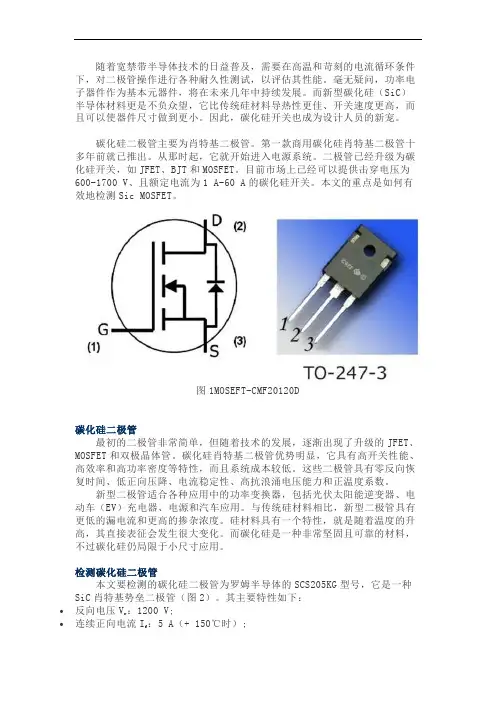
本文的重点是如何有效地检测Sic MOSFET。
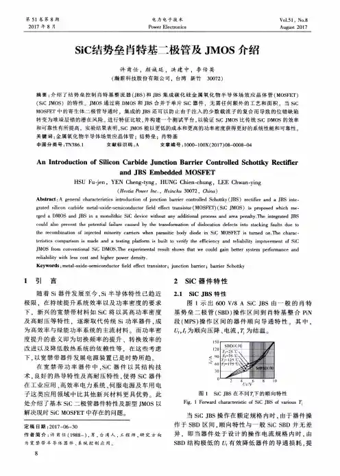
图1MOSEFT-CMF20120D碳化硅二极管最初的二极管非常简单,但随着技术的发展,逐渐出现了升级的JFET、MOSFET和双极晶体管。
碳化硅肖特基二极管优势明显,它具有高开关性能、高效率和高功率密度等特性,而且系统成本较低。
这些二极管具有零反向恢复时间、低正向压降、电流稳定性、高抗浪涌电压能力和正温度系数。
新型二极管适合各种应用中的功率变换器,包括光伏太阳能逆变器、电动车(EV)充电器、电源和汽车应用。
与传统硅材料相比,新型二极管具有更低的漏电流和更高的掺杂浓度。
硅材料具有一个特性,就是随着温度的升高,其直接表征会发生很大变化。
而碳化硅是一种非常坚固且可靠的材料,不过碳化硅仍局限于小尺寸应用。
检测碳化硅二极管本文要检测的碳化硅二极管为罗姆半导体的SCS205KG型号,它是一种SiC肖特基势垒二极管(图2)。
其主要特性如下:•反向电压V r:1200 V;•连续正向电流I f:5 A(+ 150℃时);•浪涌非重复正向电流:23 A(P W= 10ms正弦曲线,T j = + 25℃;•浪涌非重复正向电流:17 A(P W= 10ms正弦曲线,T j= + 150℃);•浪涌非重复正向电流:80 A(P W= 10μs方波,T j= + 25℃);•总功耗:88 W;•结温:+ 175℃;•TO-220AC封装。
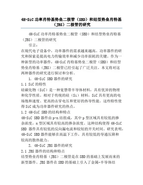
4H-SiC功率肖特基势垒二极管(SBD)和结型势垒肖特基(JBS)二极管的研究4H-SiC功率肖特基势垒二极管(SBD)和结型势垒肖特基(JBS)二极管的研究引言:在现代电子设备中,功率器件的需求越来越高。
功率器件的研究和探索是提高电力传输效率和减少功率损耗的关键。
作为一种新型的功率器件,4H-SiC肖特基势垒二极管(SBD)和结型势垒肖特基(JBS)二极管已经引起了广泛关注。
本文将对这两种器件的研究进行探讨和分析。
1. 4H-SiC SBD器件的研究1.1 SiC的特性硅碳化物(SiC)是一种宽禁带半导体材料,具有优异的物理和化学性质。
相对于传统的硅(Si)材料,SiC具有更高的电场饱和速度、更高的击穿电压和更好的热导性能。
这些特性使得SiC成为功率器件研究的热点。
1.2 4H-SiC SBD的结构和特点4H-SiC SBD器件由p-n结组成,其中p型区域具有较低的掺杂浓度,n型区域具有较高的掺杂浓度。
这种结构使得4H-SiC SBD器件具有较低的反向漏电流和较短的开关时间。
研究表明,4H-SiC SBD器件能够在高温下工作,具有较低的导通压降和较高的散热能力。
2. 4H-SiC JBS器件的研究2.1 JBS器件的结构和特点结型势垒肖特基(JBS)二极管是在SBD的基础上发展而来的新型器件。
JBS器件在SBD的基础上引入了金属-半导体结(M-S)以增强电压承受能力和抑制反向漏电流。
JBS器件的结构相对复杂,但具有较低的开关损耗和较高的可靠性。
研究表明,JBS器件在高压应用中具有较大的优势。
3. 4H-SiC SBD和JBS器件的比较3.1 性能比较研究表明,4H-SiC JBS器件相比于4H-SiC SBD器件具有更低的反向漏电流、更高的开关速度和更低的开关损耗。
这些优势使得JBS器件在高频和高压应用中具有潜在的应用前景。
3.2 制造工艺比较相对于SBD器件,JBS器件的制造工艺更为复杂,成本也较高。
Vol.32,No.6Journal of SemiconductorsJune 2011Fabrication and characteristics of a 4H-SiC junction barrier Schottky diodeChen Fengping(陈丰平) ,Zhang Yuming(张玉明),L ¨uHongliang(吕红亮),Zhang Yimen(张义门),Guo Hui(郭辉),and Guo Xin(郭鑫)School of Microelectronics,Key Laboratory of Wide Band-Gap Semiconductor Materials and Devices,Xidian University,Xi’an 710071,ChinaAbstract:4H-SiC junction barrier Schottky (JBS)diodes with four kinds of design have been fabricated and char-acterized using two different processes in which one is fabricated by making the P-type ohmic contact of the anode independently,and the other is processed by depositing a Schottky metal multi-layer on the whole anode.The re-verse performances are compared to find the influences of these factors.The results show that JBS diodes with field guard rings have a lower reverse current density and a higher breakdown voltage,and with independent P-type ohmic contact manufacturing,the reverse performance of 4H-SiC JBS diodes can be improved effectively.Furthermore,the P-type ohmic contact is studied in this work.Key words:4H-SiC;junction barrier Schottky;field guard ring DOI:10.1088/1674-4926/32/6/064003PACC:7155D;7330;7340N1.IntroductionWith increasing interest in SiC Schottky barrier diodes(SBD)in power conversion applications,much effort has been focused on improving SiC SBD performance.The junction barrier Schottky (JBS)diode offers the Schottky-like ON-state with fast switching characteristics,and the PiN-like OFF-state characteristics with low leakage current.Several SiC JBS diodes have been reported by different groups Œ1 4 .The con-duction loss can be much lower than that of a PiN diode with a breakdown voltage of less than 3kV due to the high (2.7V)turn-on voltage of the SiC P–N junction Œ5 .The leakage cur-rent of the JBS diode is lower than that of a SBD,owing to the high electric field shielded away from the Schottky contact by a depletion layer of P–N junctions.As shown in Fig.1(a),the anode contains a Schottky contact above the SBD regions and a P-type ohmic contact above the P C regions,so it is fabricated simultaneously by deposit Schottky contact metal in the cus-tomary process,as shown in Fig.1(b).In this work,two kinds of processes to fabricate the anode were employed to study the influence on the electrical characteristics of the JBS diodes.To design a JBS diode with a high breakdown voltage,several kinds of termination can be used,such as a junction termination extension and a mesa termination.However,these terminations require etching and extra ion implanting.To re-duce the processing steps and avoid the disadvantages caused by these extra steps,the filed guarding ring (FGR)was fab-ricated with P C for the main junction simultaneously in this work.The 4H-SiC JBS diodes with and without FGRs were fabricated by the two different processes mentioned above.2.Design and fabricationA 10 m N epilayer with doping of 1.56 1015cm 3was grown on the N C substrate purchased from CREE,witha doping concentration of more than 1 1018cm 3.Samples 1and 2were processed on the substrate with different tech-niques separately.First of all,the circular P C regions for the samples were formed at the same time.Multiple implantations were implemented at 400ıC in argon ambience.Al ion implan-tation was with energy of 30,280,and 500eV ,while the doses of 8.6 1013,5.2 1014,and 7.8 1014cm 2were taken,respectively.Fig.1.Schematic cross section of the JBS diodes.*Project supported by the National Natural Science Foundation of China (No.61006060)and the 13115Innovation Engineering of Shannxi Province,China (No.2008ZDKG-30).Corresponding author.Email:fpchen@Received 1November 2010,revised manuscript received 22February 2011c2011Chinese Institute of ElectronicsParameters for all structures are shown in Fig.1(a),and all of the parameters’values were chosen to be the same for both samples.The P C junctions are characterized by the width of the P C implantation window (W /and the spacing in between (S/.FGRs are characterized by the width of a single ring (L/and the spacing between the two nearest rings (D/.According to Ref.[6],L was chosen to be the fixed value 5 m,and D D 2.5 m in the experiment.For convenient description in this paper,the JBS will be marked as JBS (S ,W /.In this work,the four structures with different designs are (a)JBS (2.5,4)with-out edge termination;(b)JBS (2.5,4)terminated by FGRs;(c)JBS (3,4)without edge termination;and (d)JBS (3,4)ter-minated by FGRs.FGRs with L D 5 m for each ring were implanted around the periphery of the forward conducting ac-tive area to reduce electric field crowding at the edge of the diode under reverse bias.All of the FGRs were formed simul-taneously with the P C junction regions with ion-implantation,thus the depth and concentration are the same as the P C junc-tion regions.The samples were annealed at 1650ıC for 45min in argon ambience.Then,the profile in 0.6 m depth was mea-sured.It is well known that a high temperature annealing (>1000ıC)is usually required for ohmic contact activation.The fact that the melting temperature of Al (660ıC)is much lower gives rise to contact morphological problems.It was reported that Al melted during the high temperature anneal Œ7 ,spilling over the surface of the devices,potentially damaged the periphery of the devices.To improve the contact morphology,according to Ref.[8],a multi-layer of Ti/Al/Ti/Al/Ti/Al/Ag was deposited on sample 1’s top of P C junction regions after P C regions done,and then an annealing at 1000ıC in a gas mixture of 97%N 2and 3%H 2for 2min was carried out to create a P-type ohmic contact.Both samples underwent tri-layer metallization of Ti/Ni/Ag to form a backside contact.Sample 1was annealed for 2min and sample 2was annealed for 5min at 1000ıC in a gas mixture of 97%N 2and 3%H 2.Finally,bi-layer metallization of Ti/Ag was used to form the front Schottky metal contact for both samples.Figure 2shows the scanning electron microscope (SEM)photographs of both samples.It was previously thought that sample 2had a much better periphery than sample 1since sample 2was not annealed to make P-type ohmic contact.As can be seen in Fig.2(a),the Al spilled a little over the edge of the anode area for sample 1.This can be improved if a thinner Al layer is chosen and the Ti/Al multi-layer superposition time is increased Œ8 .3.Results and discussionThe fabricated devices were electrically measured at room temperature using a Tektronix 370B programmable curve tracer and an Agilent B1500A semiconductor device analyzer.Figure 3shows a comparison of the reverse current den-sity versus reverse voltage between JBS (2.5,4)and JBS (3,4)from each sample.As we know,when the JBS is reverse biased,the depletion layers of the adjacent P–N junctions will spread wider,leading to a reduction in the width of the Schottky chan-nel.After the depletion layer is pinched off,a potential barrier for SBD is formed,then the depletion layer is extended toward the N C substrate with further increasing reversed voltage Œ9 .Fig.2.SEM photos of both samples.(a)Sample 1.(b)Sample 2.Fig.3.Reverse V –J characteristics of JBS diodes with different val-ues of S for samples 1and 2.However,as can be seen from this figure,the current densities from sample 1have much lower reverse current densities than those of sample 2.As mentioned above,the P-type contact for sample 2is not independently fabricated,which causes the bar-rier on the P C regions to be much higher then excepted,and the depletion layers between the two nearest P C regions will not pinch off effectively.Figure 3shows a comparison between two JBS diodes with different S .Apparently,the JBS diode with S D 2.5 m has a lower reverse current density than the one with S D 3 m.It can be seen from Fig.4that the reverse current den-Fig.4.Reverse V –J characteristics of JBS diodes with and without edge termination for samples 1and 2.sity of JBS diodes with FGRs are much lower than those with-out FGRs,since FGRs can effectively reduce the field crowd-ing in the edge of devices,it has a higher breakdown voltage.In this work,JBS diodes with a breakdown voltage of up to 400V when the current density is lower than 1A/cm 2is cre-ated with FGRs Œ10 .However,the FGR structure with different ring spacing and ring widths is difficult to optimize,and in-terface charges influence the breakdown voltage significantly,since we didn’t apply any passivation layer on the surface of the devices,so the reverse current in this work is a little higher correspondingly.The dominant mechanism of reverse current depends on the Schottky barrier height,temperature,applied voltage,sur-face status,and defects in the material.According to the tech-niques we employed during manufacture,the main reasons for a relatively high leakage current and low breakdown voltage are as follows:(1)Ti is used as the metal to form the Schottky ing the thermionic emission theory,the current through the SiC Schottky diode can be expressed byI D AAT 2exp  B kT ÃÄexp qVnkT1;(1)where A is the diode area,A is the Richardson’s constant, B is the Schottky barrier height,n is the ideality factor,and other constants have their usual meanings.The forward V –J characteristics of SBD and JBS diodes are shown in Fig.5.Calculated with Eq.(1),the barrier height formed in this work is 0.79eV ,which is smaller than that fab-ricated with Ni ( B D 1.26eV)Œ11 .(2)Multi-step ion implantation brought in damages in the space lattice.(3)The epilayer material deterioration in high temperature annealing,which was stated previously.To reduce the damage during a high-temperature activation anneal,AlN can be used to prevent silicon evaporation from the 4H-SiC surface Œ12 .4.SummaryThe process that fabricates a P-type ohmic contact inde-pendently has been employed to fabricate 4H-SiC JBS diodes.Fig.5.Forward V –J characteristics of SBD and JBS diodes.The influence of FGRs in the reverse characteristics of JBSdiodes has been studied.Results show that the JBS diodes with P-type ohmic contact fabricated independently have a better performance than those by the customary process and with P+regions doping concentration ( 1 1018cm 3)and window spacing (2.5 m),4H-SiC JBS diodes using FGRs termination have a reverse current density lower than 1 10 3A/cm 2be-low 100V .References[1]Jun W,Yu D,Bhattacharya S,et al.Characterization,modelingof 10-kV SiC JBS diodes and their application prospect in X-ray generators.IEEE ECCE,2009,20:1488[2]Yan G,Huang A Q,Agarwal A K,et al.Integration of 1200VSiC BJT with SiC diode.20th ISPSD,2008,18:233[3]Hull B A,Sumakeris J J,O’Loughlin M J,et al.Performance andstability of large-area 4H-SiC 10-kV junction barrier Schottky rectifiers.IEEE Trans Electron Devices,2008,55(8):1864[4]Feng Z,Mohammad M I,Biplob K D,et al.Effect of crystallo-graphic dislocations on the reverse performance of 4H-SiC p–n diodes.Mater Lett,2010,64(3):281[5]Lin Z,Chow T P,Jones K A,et al.Design,fabrication,and char-acterization of low forward drop,low leakage,1-kV 4H-SiC JBS rectifiers.IEEE Trans Electron Devices,2006,53(2):363[6]Cao L H.4H-SiC gate turn-off thyristor and merged P–i–N andSchottky barrier diode.PhD Thesis,New Jersey,Rutgers Univer-sity New Brunswick,2000[7]Luo Y ,Yan F,Tone K,et al.Searching for device processingcompatible ohmic contacts to implanted P-type 4H-SiC.Proceed-ings of the International Conference on Silicon Carbide and Re-lated Materials,1999,338:1013[8]Jennings M R,P ´e rez-Tom ´a s A,Davies M,et al.Analysis of Al/Ti,Al/Ni multiple and triple layer contacts to P-type 4H-SiC.Solid-State Electron,2007,51(5):797[9]Zhang Y M,Zhang Y M,Alexandrov P,et al.Fabrication of 4H-SiC merged PN-Schottky diodes.Chinese Journal of Semicon-ductors,2001,22(3):265[10]Chen F P,Zhang Y M,Zhang Y M,et al.Study of 4H-SiC junc-tion barrier Schottky diode using field guard ring termination.Chin Phys B,2010,19(9):097107[11]Zhang L,Zhang Y M,Zhang Y M,et al.Gamma-ray radiationeffect on Ni/4H-SiC SBD.Acta Phys Sin,2009,58(4):2737[12]Jones K A,Shah P B,Kirchner K W,et al.Annealing ion im-planted SiC with an AlN cap.Mater Sci Eng,1999,61:281。

碳化硅mosfet的集成式体二极管-概述说明以及解释1.引言1.1 概述概述部分可以介绍碳化硅MOSFET和集成式体二极管的背景和意义。
碳化硅MOSFET是一种新型的功率器件,具有较高的开关速度、较低的导通电阻和较高的工作温度等优势。
其主要应用领域包括电动车辆、太阳能和风能发电系统等。
随着碳化硅半导体材料的发展和成熟,碳化硅MOSFET已经成为了替代传统硅功率器件的热门选择。
而集成式体二极管是一种结合了功率MOSFET和快速恢复二极管的器件,通过优化二极管与MOSFET的布局和工艺,可以实现更低的开关损耗和更高的开关速度。
集成式体二极管的应用范围广泛,特别适用于需要高效能转换和快速开关的场合,如电源供应、电动车辆和工业自动化等领域。
本文将重点介绍碳化硅MOSFET与集成式体二极管的结合意义以及其带来的优势。
同时,将探讨碳化硅MOSFET与集成式体二极管的发展前景和应用领域,为读者提供更深入的了解和应用指导。
1.2 文章结构文章结构是指文章的组织框架和内容安排,通过清晰的结构可以使读者更好地理解文章的主题和观点。
本文的结构主要包括引言、正文和结论三个部分。
引言部分概述了本文要讨论的内容,介绍了碳化硅MOSFET的集成式体二极管这一主题,并说明了文章的目的。
在本文中,我们将首先介绍碳化硅MOSFET的基本原理,然后深入探讨集成式体二极管的基本原理。
最后,我们将分析和讨论碳化硅MOSFET与集成式体二极管的结合意义,并展望其发展前景与应用。
正文部分将详细介绍碳化硅MOSFET的基本原理。
我们将讨论碳化硅材料的特点以及其在MOSFET中的应用前景。
同时,我们将解释碳化硅MOSFET的工作原理和关键特性,包括高温特性、高电压特性和高频特性等。
接着,我们将探讨集成式体二极管的基本原理。
首先,我们将介绍集成式体二极管的概念和优势,解释其与传统二极管的区别。
然后,我们将详细讲解集成式体二极管的工作原理和特性,包括正向导通和反向截止特性等。
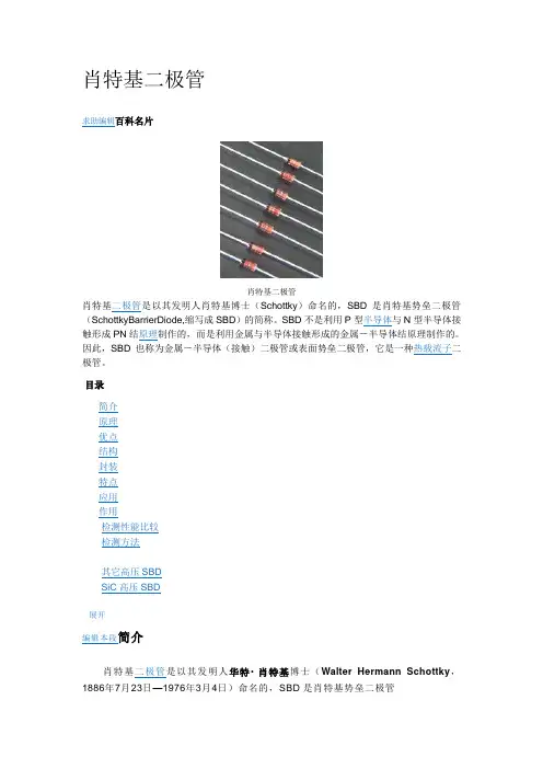
肖特基二极管求助编辑百科名片肖特基二极管肖特基二极管是以其发明人肖特基博士(Schottky)命名的,SBD是肖特基势垒二极管(SchottkyBarrierDiode,缩写成SBD)的简称。
SBD不是利用P型半导体与N型半导体接触形成PN结原理制作的,而是利用金属与半导体接触形成的金属-半导体结原理制作的。
因此,SBD也称为金属-半导体(接触)二极管或表面势垒二极管,它是一种热载流子二极管。
目录简介原理优点结构封装特点应用作用检测性能比较检测方法其它高压SBDSiC高压SBD展开编辑本段简介肖特基二极管是以其发明人华特‧肖特基博士(Walter Hermann Schottky,1886年7月23日—1976年3月4日)命名的,SBD是肖特基势垒二极管肖特基二极管结构原理图(Schottky Barrier Diode,缩写成SBD)的简称。
SBD不是利用P型半导体与N型半导体接触形成PN结原理制作的,而是利用金属与半导体接触形成的金属-半导体结原理制作的。
因此,SBD也称为金属-半导体(接触)二极管或表面势垒二极管,它是一种热载流子二极管。
肖特基二极管是近年来问世的低功耗、大电流、超高速半导体器件。
其反向恢复时间极短(可以小到几纳秒),正向导通压降仅0.4V左右,而整流电流却可达到几千毫安。
这些优良特性是快恢复二极管所无法比拟的。
中、小功率肖特基整流二极管大多采用封装形式。
编辑本段原理肖特基二极管肖特基二极管是贵金属(金、银、铝、铂等)A为正极,以N型半导体B为负极,利用二者接触面上形成的势垒具有整流特性而制成的金属-半导体器件。
因为N型半导体中存在着大量的电子,贵金属中仅有极少量的自由电子,所以电子便从浓度高的B中向浓度低的A中扩散。
显然,金属A中没有空穴,也就不存在空穴自A向B的扩散运动。
随着电子不断从B扩散到A,B表面电子浓度逐渐降低,表面电中性被破坏,于是就形成势垒,其电场方向为B→A。
SiC结势垒肖特基二极管总结报告何东(B140900200)肖凡(B140900208)于佳琪(B140900204)一、SiC JBS器件的发展现状1. 宽禁带半导体材料的优势当前,随着微电子器件向低功耗、高耐压、高可靠性方向的发展,对半导体材料的要求也逐渐提高。
微电子器件越来越多的应用在高温、高辐照、高频和大功率等特殊环境。
为了满足微电子器件在耐高温和抗辐照等领域的应用,需要研发新的半导体材料,从而最大限度地提高微电子器件性能。
传统的硅器件和砷化镓器件限制了装置和系统性能的提高。
以碳化硅(SiC)和氮化镓(GaN)为代表的第三代半导体材料,由于材料本身的宽禁带宽度和高临界击穿电场等优点成为制作耐高温、高功率和抗辐照等电子器件的理想的半导体材料[1]。
目前研究的SiC基器件有高温和功率SiC器件、微波和高频SiC器件、SiC光电器件、抗辐照器件等[2]。
SiC材料的临界击穿场强是Si材料的10倍,SiC的禁带宽度和热导率均是Si材料的3倍,本征载流子的浓度也只有硅材料的十分之一。
这些优异的物理特性使SiC材料制成的半导体功率器件在高频、高温、大功率及高辐照等环境下有很高的优势。
SiC在不同的环境下能形成不同的晶体结构,现在常用的有3C-SiC、4H-SiC、6H-SiC三种晶体结构。
4H-SiC材料以其较高的禁带宽度和空穴迁移率,较低的本征载流子浓度成为制造半导体器件的主流材料[3-4]。
具备以上优异的物理特性的4H-SiC材料主要有以下应用:(1)利用其优异的热导率特性,在器件封装及温度方面的要求低,4H-SiC 器件适合应用在卫星、航空和航天探测、石油以及地热钻井探测、汽车发动机等需要耐高温的环境中。
(2)利用其宽禁带宽度和高化学稳定性,在高频和抗辐照等领域,4H-SiC 器件具有不可替代的作用,因为它可以抵御强大的射线辐射,在核战或强电磁干扰中的耐受能力远远超过硅基器件。
(3)利用其高的饱和速度和临界击穿场强,4H-SiC是1~10 GHz范围的大功率微波放大器的理想应用材料,高频和微波4H-SiC器件在军用雷达、通信和广播电视等领域具有很好的应用前景。
宇航用sic结势垒肖特基二极管单粒子效应研究宇航用SiC结势垒肖特基二极管单粒子效应研究近年来,随着航天技术的不断发展和深入研究,宇航领域对高性能电子器件的需求越来越高。
在宇航器件中,具有高速、高温、高辐射环境下可靠性强的特点的电子器件至关重要。
而SiC(碳化硅)结势垒肖特基二极管正是满足这一需求的理想选择。
它能够在极端环境下表现出优异的性能,被广泛应用于宇航用电子器件中。
一、SiC结势垒肖特基二极管的特性1. 高温特性SiC材料具有良好的高温特性,能够在宇航器件运行过程中承受高温环境的考验。
相比于传统的硅材料,SiC具有更高的熔点和更好的热导率,能够稳定地工作在高温环境下,不易失效。
2. 高速特性SiC材料的载流子迁移率高,电子与空穴的迁移速度快,使得SiC结势垒肖特基二极管具有较高的开关速度和响应速度。
这使得其尤为适合在高频率下工作,并能满足宇航领域对高速通信和信号处理方面的要求。
3. 高辐射抗损伤能力在宇航环境中,辐射是一种普遍存在的影响因素。
传统的硅材料容易受到辐射的影响而损伤,导致电子器件的性能下降。
而SiC材料由于具有较高的辐射抗损伤能力,能够在辐射环境中保持其良好的性能。
4. 低漏电流SiC结势垒肖特基二极管的漏电流较低,这是因为它具有较高的击穿电场强度和较低的面积漏电流密度。
在宇航器件中,低漏电流可以提高能量效率,并减少能源消耗。
二、肖特基二极管单粒子效应研究1. 单粒子效应的定义在电子器件中,单粒子效应是指当宇宙射线或辐射颗粒进入设备中,并在其中产生电子或空穴对时,导致器件的电学性能发生瞬态或永久性的改变。
单粒子效应是宇航电子器件中一个重要的研究方向,对保证宇航器件的可靠性和稳定性非常关键。
2. SiC结势垒肖特基二极管的单粒子效应研究SiC结构材料具有较好的辐射抗损伤能力,因此对于宇航器件中的单粒子效应研究具有重要意义。
通过对SiC结势垒肖特基二极管在单粒子辐射下的响应性能进行研究,可以评估其对宇航辐射环境的适应性和稳定性,为宇航电子器件的设计和制造提供指导和支持。