CT4502型军用多芯组陶瓷电容器pdf
- 格式:pdf
- 大小:1.55 MB
- 文档页数:4
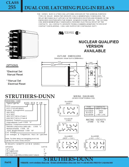
255RUL R ecognized File No. E 13224RTHE S E R IE S B 255 IS A TWO C OIL LATC HING VE R S ION OF THE G E NE R AL P UR P OS E TY P E 219 R E LAY. WHE N THE OP E R ATE C OIL IS MOME NTAR ILY E NE R G IZE D, THE R E LAY ME C HANIC ALLY LATC HE S IN THE E NE R G IZE D P OS ITION AND R E MAINS IN THE E NE R G IZE D P OS ITION WITH THE P OWE R R E MOVE D F R OM THE C OIL. THE S E C OND C OIL WHE N MOME NTAR LY E NE R G IZE D, P R OVIDE S E LE C TR IC AL R E S E T OF THE C ONTAC TS. ALL C ONTAC TS OP E R ATE F R OM A C OMMON AR MATUR E TO P R E VE NT C ONTAC T OVE R LAP P ING. C OILS AR E R ATE D F OR C ONTINUOUS DUTY.U V L M 33S UF F IXOP TIONS130 C C oilC oil S uppression Light & ActuatorF ine S ilver-G old Diffused B ifurcated C ontactsB 255 XC X P L M -S eriesB255 2 C oil Latch plug-in C ontact Arrangements XB X DP DT XC X 3P DTAB X S P S T-NO & 2 F orm C B XB DP S T-NO & 2 F orm B S tandard F eaturesP olycarbonate C over- C ODE "P "Optional F eaturesIndicator Lamp across both coils - C ODE "L " Manual Actuator- C ODE "M" P erm. Magnet B lowout - C ODE "69"C oil VoltageC oil Voltages & F requencies mus t be s pecified.Note: F or time delay on energizing reset coil,specify 256 series in lieu of B 255OR DE R ING C ODE Typical Type No.DC R E LAY S , 1.8 WATTS (2.5 W @ 125VDC )PAGEWEBSITE: EMAIL:info@ FAX # 1-843-662-8862 PHONE # 1-843-664-3303C ONTAC TS61712B 255XB XP (DP DT )61712B 255XC XP (3 P DT)61712B 255AB XP (DP DT + 1 N.O. )R E S E TO P E R A T EO P E R A T ER E S E TR E S E TO P E R A T E61712B 255B XB P (2 N.O. + 2 N.C. )R E S E TO P E R A T EB 255AB XP B 255XB XP B 255XC P B 255B XB PDP DT + 1 NODP DT 3P DT 2 NO + 2 NCWIR ING DIAG R AMS(VIE WE D F R OM TE R MINAL E ND)TY P E4.56(115.8)12167L O C K I N G D E V I C E2.625(66.67)1.468(37.28)3.75(95.25)OUTL INE DIME NS IONSDimensions shown Inch & (Millimeters)MATING S OC K E TS 27390 - 12 P INSTRUTHERS-DUNNSTRUTHERS-DUNN DUAL COIL LATCHING PLUG-IN RELAYSCLASSNUCLEAR QUALIFIED VERSION AVAILABLEOPTIONS*Electrical Set Manual Reset* Manual Set Electrical ResetWE B S ITE : www.s truthers E MAIL:info@ms truthers FAX # 1-843-662-8862 PHONE # 1-843-664-330385% of Nominal Voltage 80 % of Nominal Voltage 110% of nominal, voltageS ilver Alloy & G old Diffused (S tandard)25 mS Max. @ Nominal Voltage.20 mS Max. @ Nominal Voltage.1500 V rms1/4" over surface, 1/8" thru Air-10 C to +60 C10 Million Operations no load100,000 Operations @ R ated Load.500,000 Operations 1/2 R ated Load.C lear polycarbonate.215 g (7.58 oz.) AP P R OX.G E NE R AL S P E C IF IC ATIONSC OIL P ull-in, min. AC P ull-in min. DC Overvoltage, max.C ONTAC TSC ontact Material:TIMINGOperate Time: (operate coil) R elease Time: (R eset coil energized)DIE L E C TR IC S TR E NG THAll Mutually Insulated P oints: Insulation :TE MP E R ATUR E R ated Operation:L IF E E XP E C TANC Y Mechanical: E lectrical:MIS C E L L ANE OUS E nclosure: Weight:RUL R ecognized File No. E 13224R3.014.552.01450500084025615026.54.8 1.104.2015.5540181561224120240R esistance Ohms ± 10%C oil P ower (mA)Nominal Voltage R esistance Ohms ± 10%C oil P ower(mA)80041020045.013.2R E S E T C OIL (3VA)OP E R ATE C OIL (5VA)*AC C OIL , 50/60 HZC OIL S P E C IF IC ATIONS @ 25 C C urrent inrush on all AC coils is less than twice the listedmilliamperes ratings as shown in the AC coil data table.*C urrents shown in table measured at 60 Hz.61224115/125Nominal Voltage DC relays, 1.8 Watts (2.5 W @ 125VDC )DC C OIL DATAR E S E T C OIL 1.4W)38518996.020.015.563.525062002861418014.421.085.03008000R esistance Ohms ± 10%C oil P ower (mA)OP E R ATE C OIL (1.8W)R esistanceOhms± 10%C oil P ower(mA)10A 3A 1A 3A 0.1A0.5A 1.5A 150 mA 0.5A24 VDC 120 VAC 240 VAC 28 VDC 125 VDC125 VDC S M 125 VDC DM 250 VDC S M 250 VDC DMVOLTSMAK E 30A 30A 30A 30A 30A30A 30A 30A 30A10A 10A 10A 10A 10A10A 10A 10A 10A10A 10A 5A 10A 0.5A1.5A 4A 0.5A 1.5AR E S IS TIVE INDUC TIVEC AR R Y B R E AKC ONTAC T R ATING S** F or vers ions with s uffix "69" P ermanent Magnet B lowouts**R elays with C ode 69 feature ( C heck with factory for UL & C S A Listing).PAGESTRUTHERS-DUNN00255DUAL COIL LATCHING PLUG-IN RELAYSCLASS。
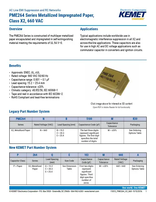
Benefits• Approvals: ENEC, UL, cUL• Rated voltage: 660 VAC 50/60 Hz • Capacitance range: 0.001 – 0.1 µF • Lead spacing: 15.2 – 25.4 mm • Capacitance tolerance: ±20%• Climatic category: 40/85/56, IEC 60068–1• Tape and reel in accordance with IEC 60286–2• RoHS Compliant and lead-free terminationsOverviewThe PME264 Series is constructed of multilayer metallized paper encapsulated and impregnated in self-extinguishing material meeting the requirements of UL 94 V–0.ApplicationsTypical applications include worldwide use inelectromagnetic interference suppression in all X2 and across-the-line applications. These capacitors are also for use in high AC and DC voltage applications such as commutator capacitor in converters and ignition circuits.AC Line EMI Suppression and RC NetworksPME264 Series Metallized Impregnated Paper, Class X2, 660 VACLegacy Part Number SystemNew KEMET Part Number SystemClick image above for interactive 3D contentOpen PDF in Adobe Reader for full functionalityOrdering Options Table Benefits cont'd• Operating temperature range of −40˚C to +85˚C• 100% screening factory test at 3,000 VDC• The highest possible safety regarding active and passive flammability• Excellent self-healing properties ensure long life even when subjected to frequent over-voltages • Good resistance to ionization due to impregnated dielectric • High dV/dt capability• The impregnated paper ensures excellent stability and outstanding reliability properties, especially in applications with continuous operationDimensions – MillimetersFRONT VIEW SIDE VIEWPerformance CharacteristicsEnvironmental Test DataApprovalsEnvironmental ComplianceAll KEMET EMI capacitors are RoHS Compliant.Table 1 – Ratings & Part Number Reference(1) Insert ordering code for lead type and packaging. See Ordering Options Table for available options.Soldering ProcessThe implementation of the RoHS directive has resulted in the selection of SnAgCu (SAC) alloys or SnCu alloys as primary solder. This has increased the liquidus temperature from that of 183ºC for SnPb eutectic alloy to 217 – 221ºC for the new alloys. As a result, the heat stress to the components, even in wave soldering, has increased considerably due to higher pre-heat and wave temperatures. Polypropylene capacitors are especially sensitive to heat (the melting point of polypropylene is 160 – 170ºC). Wave soldering can be destructive, especially for mechanically small polypropylene capacitors (with lead spacing of 5 mm to 15 mm), and great care has to be taken during soldering. The recommended solder profiles from KEMET should be used. Please consult KEMET with any questions. In general, the wave soldering curve from IEC Publication 61760-1 Edition 2 serves as a solid guideline for successful soldering. Please see Figure 1.Reflow soldering is not recommended for through-hole film capacitors. Exposing capacitors to a soldering profile in excess of the above the recommended limits may result to degradation or permanent damage to the capacitors.Do not place the polypropylene capacitor through an adhesive curing oven to cure resin for surface mount components. Insert through-hole parts after the curing of surface mount parts. Consult KEMET to discuss the actual temperature profile in the oven, if through-hole components must pass through the adhesive curing process. A maximum two soldering cycles is recommended. Please allow time for the capacitor surface temperature to return to a normal temperature before the second soldering cycle.Manual Soldering Recommendations Following is the recommendation for manual soldering with a soldering iron.The soldering iron tip temperature should be set at 350°C (+10°C maximum) with the soldering duration not to exceed more than 3 seconds.Recommended Soldering TemperatureSoldering time (sec)S o l d e r i n g i r o n b i t t e m p e r a t u r e (d e g C )0501001502002503004080120160200240T e m p e r a t u r e (°C )Time (s)Soldering Process cont'dWave Soldering Recommendations cont'd1. The table indicates the maximum set-up temperature of the soldering processFigure 12. The maximum temperature measured inside the capacitor:Set the temperature so that inside the element the maximum temperature is below the limit:Temperature monitored inside the capacitor.Selective Soldering RecommendationsSelective dip soldering is a variation of reflow soldering. In this method, the printed circuit board with through-holecomponents to be soldered is preheated and transported over the solder bath as in normal flow soldering without touching the solder. When the board is over the bath, it is stopped and pre-designed solder pots are lifted from the bath with molten solder only at the places of the selected components, and pressed against the lower surface of the board to solder the components.The temperature profile for selective soldering is similar to the double wave flow soldering outlined in this document, however, instead of two baths, there is only one bath with a time from 3 to 10 seconds. In selective soldering, the risk ofoverheating is greater than in double wave flow soldering, and great care must be taken so that the parts are not overheated.ConstructionDetailed Cross SectionSelf-ExtinguishingSelf-ExtinguishingResinMetal ContactLayerMetal ContactLayerMarginMetallized Impregnated Paper(First Layer)MarginMetallized Impregnated Paper(Second Layer)Metal Spraying Impregnated Series Design — Multilayer Impregnated Paper Dielectric2 SectionWinding SchemeMarkingBACKFRONTTOPSeriesSelf HealingPackaging QuantitiesLead Taping & Packaging (IEC 60286–2)Taping Specifi cation(1) Maximum cumulative feed hole error, 1 mm per 20 parts.(2) 16.5 mm available on request.(3) Depending on case size.(4) 15 mm available on request.Lead Taping & Packaging (IEC 60286–2) cont'd Ammo Specifi cationsReel Specifi cationsManufacturing Date Code (IEC–60062)KEMET Electronic Corporation Sales Offi cesFor a complete list of our global sales offi ces, please visit /sales.DisclaimerAll product specifi cations, statements, information and data (collectively, the “Information”) in this datasheet are subject to change. The customer is responsible for checking and verifying the extent to which the Information contained in this publication is applicable to an order at the time the order is placed.All Information given herein is believed to be accurate and reliable, but it is presented without guarantee, warranty, or responsibility of any kind, expressed or implied. Statements of suitability for certain applications are based on KEMET Electronics Corporation’s (“KEMET”) knowledge of typical operating conditions for such applications, but are not intended to constitute – and KEMET specifi cally disclaims – any warranty concerning suitability for a specifi c customer application or use. The Information is intended for use only by customers who have the requisite experience and capability to determine the correct products for their application. Any technical advice inferred from this Information or otherwise provided by KEMET with reference to the use of KEMET’s products is given gratis, and KEMET assumes no obligation or liability for the advice given or results obtained.Although KEMET designs and manufactures its products to the most stringent quality and safety standards, given the current state of the art, isolated component failures may still occur. Accordingly, customer applications which require a high degree of reliability or safety should employ suitable designs or other safeguards (such as installation of protective circuitry or redundancies) in order to ensure that the failure of an electrical component does not result in a risk of personal injury or property damage.Although all product–related warnings, cautions and notes must be observed, the customer should not assume that all safety measures are indicted or that other measures may not be required.KEMET is a registered trademark of KEMET Electronics Corporation.。

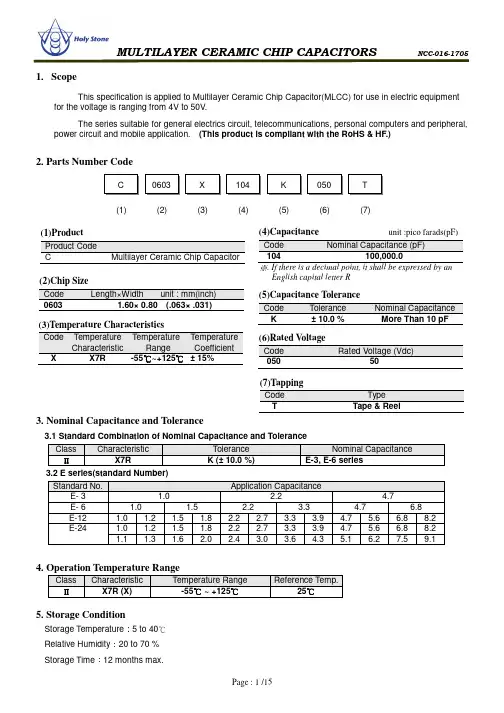
1. ScopeThis specification is applied to Multilayer Ceramic Chip Capacitor(MLCC) for use in electric equipment for the voltage is ranging from 4V to 50V.The series suitable for general electrics circuit, telecommunications, personal computers and peripheral, power circuit and mobile application. (This product is compliant with the RoHS & HF.)2. Parts Number Code3. Nominal Capacitance and Tolerance3.1 Standard Combination of Nominal Capacitance and ToleranceClass CharacteristicTolerance Nominal CapacitanceⅡX7RK (± 10.0 %)E-3, E-6 series3.2 E series(standard Number) Standard No.Application CapacitanceE- 3 1.02.24.7E- 6 1.0 1.52.23.34.76.8E-12 1.0 1.2 1.5 1.8 2.2 2.7 3.3 3.9 4.7 5.6 6.8 8.2 E-241.0 1.2 1.5 1.82.2 2.73.3 3.94.75.66.8 8.2 1.1 1.31.62.02.43.0 3.64.35.16.27.5 9.14. Operation Temperature RangeClassCharacteristic Temperature Range Reference Temp.Ⅱ X7R (X)-55 ~ +125℃℃25℃5. Storage ConditionStorage Temperature :5 to 40℃ Relative Humidity :20 to 70 % (6)Rated Voltage Code Rated Voltage (Vdc)05050 (1) (2) (3) (4) (5) (6) (7) (1)ProductProduct CodeC Multilayer Ceramic Chip Capacitor(3)Temperature Characteristics Code Temperature Characteristic Temperature Range Temperature Coefficient X X7R -55℃~+125℃ ± 15% (4)Capacitance unit :pico farads(pF)Code Nominal Capacitance (pF) 104 100,000.0 ※. If there is a decimal point, it shall be expressed by an English capital letter R(5)Capacitance Tolerance Code Tolerance Nominal CapacitanceK ± 10.0 % More Than 10 pF (7)TappingCode TypeT Tape & Reel(2)Chip Size Code Length×Width unit : mm(inch) 06031.60× 0.80 (.063× .031)6. Dimensions6.1 Configuration and Dimension :Unit:mmTYPE LW TB (min)BW (min) 06031.60± 0.100.80± 0.100.85± 0.150.400.156.2 Termination Type :External Electrodes BarrierInner ElectrodesPolymer Electrodes (If applicable)7. PerformanceWhen operating at temperature range from 100℃to 125℃, the operation shall be carried out at a derating voltage or less as shown belowFig.1P.C. Board for Bending Strength TestMaterial : Glass Epoxy Substrate: Solder ResistTest SubstrateMaterial : Glass Epoxy Substrate: Copper (Thickness : 0.035mm)Thickness : 1.6 mmUnit:mmType A B C 0201 0.2 0.9 0.4 0402 0.5 1.5 0.6 0603 1.0 3.0 1.0 0805 1.2 4.0 1.6 1206 2.2 5.0 2.0 1210 2.2 5.0 2.9 1808 3.5 7.0 2.5 1812 3.5 7.0 3.7 2208 4.5 8.0 2.5 2211 4.5 8.0 3.0 22204.58.05.68. Packing8.1 Bulk PackingAccording to customer request. 8.2 Chip Capacitors Tape Packing8.3 Material And QuantityTape Material 0201 0402 0603/0805 T 0.≦33mm T 0.55mm ≦ T ≦1.00mm T >1.00mm Paper 15,000 pcs/Reel 10,000 pcs/Reel 4,000 pcs/Reel NAPlastic NA NA NA 3,000 pcs/ReelTape Material 1206T ≦1.00mm 1.00mm <T 1.25mm ≦T >1.25mmPaper 4,000 pcs/ReelNANAPlastic NA3,000 pcs/Reel2,000 pcs/ReelTape Material 1808/1210T ≦1.25mm1.25mm <T ≦2.40mmT >2.40mmPaper NANANAPlastic 3000 pcs/Reel2000 pcs/Reel500/1,000 pcs/ReelTape Material 1812/2211/2220 1825/2225 2208 T ≦2.20mm T >2.20mm T ≦2.20mm T >2.20mm T ≦2.20mm Paper NA NA NA NA NAPlastic 1000 pcs/Reel 700 pcs/Reel 700 pcs/Reel400 pcs/Reel 1000 pcs/Reel NA :Not Available8.4 Cover Tape Reel Off Force8.4.1 Peel-Off Force5 g·f Peel ≦-Off Force 70 g ≦·f 8.4.2 Measure Method8.5 Paper TapeUnit:mm8.6 Plastic TapeUnit:mm TYPE A B C DE 0201 0.37± 0.1 0.67± 0.1 4.00± 0.1 2.00± 0.052.00± 0.10402 0.61± 0.1 1.20± 0.1 0603 1.10± 0.2 1.90± 0.2 4.00± 0.10805 1.50± 0.2 2.30± 0.2 1206 1.90± 0.2 3.50± 0.2 1210 2.90± 0.2 3.60± 0.2 TYPE FG H It0201 1.75± 0.103.50± 0.058.0± 0.30 φ1.50 +0.10/-0 1.10 max.0402 0603 0805 1206 1210Type A B C D E F 0805 1.5±0.2 2.3±0.2 4.0± 0.12.0± 0.054.0± 0.11.75± 0.11206 1.9±0.2 3.5±0.2 1210 2.9±0.2 3.6±0.2 1808 2.5±0.2 4.9±0.2 1812 3.6±0.2 4.9±0.2 8.0± 0.11825 6.9±0.2 4.9±0.2 2208 2.5±0.2 6.1±0.2 2211 3.2±0.2 6.1±0.2 2220 5.4±0.2 6.1±0.2 22256.9±0.26.1±0.28.7 Reel DimensionsReel Material :PolystyreneType G H IJ t O 0805 3.5± 0.058.0± 0.3φ1.5+0.1/-03.0 max.0.3 max.1.0± 0.11206 1210 1808 5.5± 0.05 12.0 ± 0.3 4.0 max. 1.5± 0.11812 1825 2208 2211 2220 2225Type AB C DE W 0201 φ382 max φ50 min φ13± 0.5φ21± 0.82.0±0.510± 0.150402 0603 0805 1206 1210 1808 φ178±0.2 φ60±0.2 13±0.31812 1825 2208 2211 2220 2225Unit:mmPrecautionary Notes:1. StorageStore the capacitors where the temperature and relative humidity don’t exceed 40°C and 70%RH. Werecommend that the capacitors be used within 12 months from the date of manufacturing. Store the products in the original package and do not open the outer wrapped, polyethylene bag, till just before usage. If it is open, seal it as soon as possible or keep it in a desiccant with a desiccation agent.2. Construction of Board PatternImproper circuit layout and pad/land size may cause excessive or not enough solder amount on the PC board. Not enough solder may create weak joint, and excessive solder may increase the potential of mechanical or thermal cracks on the ceramic capacitor. Therefore we recommend the land size to be as shown in the following table: 2.1 Size and recommend land dimensions for reflow soldering2.2 Mechanical strength varies according to location of chip capacitors on the P .C. board.Design layout of components on the PC board such a way to minimize the stress imposed on the components, upon flexure of the boards in depanelization or other processes.Component layout close to the edge of the board or the “depanelization line” is not recommended. Susceptibility to stress is in the order of: a>b>c and d>eEIA Code Chip (mm) Land (mm) L W A B C D E 0201 0.60 0.30 0.2~0.3 0.2~0.4 0.2~0.4 -- -- 0402 1.00 0.50 0.3~0.5 0.3~0.5 0.4~0.6 -- -- 0603 1.60 0.80 0.4~0.6 0.6~0.7 0.6~0.8 -- -- 0805 2.00 1.25 0.7~0.9 0.6~0.8 0.8~1.1 -- -- 1206 3.20 1.60 2.2~2.4 0.8~0.9 1.0~1.4 1.0~2.0 3.2~3.7 1210 3.20 2.50 2.2~2.4 1.0~1.2 1.8~2.3 1.0~2.0 4.1~4.6 1808 4.60 2.00 2.8~3.4 1.8~2.0 1.5~1.8 1.0~2.8 3.6~4.1 1812 4.60 3.20 2.8~3.4 1.8~2.0 2.3~3.0 1.0~2.8 4.8~5.3 1825 4.60 6.35 2.8~3.4 1.8~2.0 5.1~5.8 1.0~4.0 7.1~8.3 2208 5.70 2.00 4.0~4.6 2.0~2.2 1.5~1.8 1.0~4.0 3.6~4.1 2211 5.70 2.80 4.0~4.6 2.0~2.2 2.0~2.6 1.0~4.0 4.4~4.9 2220 5.70 5.00 4.0~4.6 2.0~2.2 3.5~4.8 1.0~4.0 6.6~7.1 2225 5.70 6.354.0~4.62.0~2.2 5.1~5.8 1.0~4.07.1~8.32.3 Layout Recommendation3. Mounting3.1 Sometimes crack is caused by the impact load due to suction nozzle in pick and place operation.In pick and place operation, if the low dead point is too low, excessive stress is applied to component. This maycause cracks in the ceramic capacitor, therefore it is required to move low dead point of a suction nozzle to the higher level to minimize the board warp age and stress on the components. Nozzle pressure is typically adjusted to 1N to 3N (static load) during the pick and place operation.3.2 Amount of Adhesivea0.2mm min. b 70 ~ 100 µm cDo not touch the solder landExample : 0805 & 12064. Soldering4.1. Wave SolderingMost of components are wave soldered with solder at 230 to 250°C. Adequate care must be taken to prevent the potential of thermal cracks on the ceramic capacitors. Refer to the soldering methods below for optimum soldering benefits.Recommend flow soldering temperature ProfileTo optimize the result of soldering, proper preheating is essential: 1) Preheat temperature is too low a. Flux flows to easilyb. Possibility of thermal cracks2) Preheat temperature is too higha. Flux deteriorates even when oxide film is removedb. Causes warping of circuit boardc. Loss of reliability in chip and other componentsCooling Condition:Natural cooling using air is recommended. If the chips are dipped into a solvent for cleaning, the temperature difference (ΔT) between the solvent and the chips must be less than 100°C.4.2 Reflow SolderingPreheat and gradual increase in temperature to the reflow temperature is recommended to decrease the potential of thermal crack on the components. The recommended heating rate depends on the size of component, however it should not exceed 3°C/Sec.Recommend reflow profile for Lead-Free soldering temperature Profile (MIL-STD-202G #210F)Soldering Method Change in Temp.( )℃1206 and Under ΔT 190 ≦℃ 1210 and Over ΔT 130 ≦℃Soldering Method Change in Temp.( )℃ 1206 and UnderΔT ≤ 100~130 max.SolderingT e m p e r a t u r e (°C )T e m p e r a t u r e (°C )※ The cycles of soldering : Twice (max.)4.3 Hand SolderingSudden temperature change in components, results in a temperature gradient recommended in the following table, and therefore may cause internal thermal cracks in the components. In general a hand soldering method is not recommended unless proper preheating and handling practices have been taken. Care must also be taken not to touch the ceramic body of the capacitor with the tip of solder Iron.Soldering Method Change in Temp.( )℃1206 and Under ΔT 1≦50 ℃1210 and Over ΔT 130≦℃How to Solder Repair by Solder Iron1) Selection of the soldering iron tipThe required temperature of solder iron for any type of repair depends on the type of the tip, the substrate material, and the solder land size.2) recommended solder iron conditiona.) Preheating Condition:Board and components should be preheated sufficiently at 150°C or over,and soldering should be conducted with soldering iron as boards and components are maintainedat sufficient temperatures.b.) Soldering iron power shall not exceed 30 W.c.) Soldering iron tip diameter shall not exceed 3mm.d.) Temperature of iron tip shall not exceed 350°C to perform the process within 5 seconds.(refer to MIL-STD-202G)f.) Do not touch the ceramic body with the tip of solder iron. Direct contact of the soldering iron tip to ceramicbody may cause thermal cracks.g.) After soldering operation, let the products cool down gradually in the room temperature.5. Handling after chip mounted5.1 Proper handling is recommended, since excessive bending and twist of the board, depends on the orientationof the chip on the board, may induce mechanical stress and cause internal crack in the capacitor.Temperature(°C)200→Higher potential of crack Lower potential of crack ╳5.3 Mechanical stress due to warping a (a) Crack occurrence ratio will be in (b) Crack occurrence ratio will be in :Tensile Stress ╳6. Handling of Loose Chip Capacitor 6.1 If dropped the chip capacitor may c6.2 In piling and stacking of the P .C. bo may hit the chip capacitor mounted7. Safekeeping condition and period For safekeeping of the products, we re under humidity of 20 to 70% RH. The sing and torsion.be increased by manual separation.be increased by tensile force , rather than compressiv s○ :Compressive Stress tor may crack. .C. boards after mounting for storage or handling, the unted on another board to cause crack.we recommend to keep the storage temperature betwe The shelf life of capacitors is 12 months. ressive force.ess, the corner of the P .C. boardbetween +5 to +40°C and Crack。

配电型避雷器HY5WS:保护相应电压等级的开关柜、变压器、箱式变、电缆头等有关配电设备免受大气和操作过电压损坏。
电站型避雷器HY5WZ:保护发电厂、变电所中交流电器设备免受大气过电压和操作过电压的损坏。
按以上讲,开关柜中应该用S型,那么Z型用在哪里?有的按进线用Z型,除电机、电容外的馈出用S型,正确选择安装金属氧化物避雷器1 10kV配电网中的金属氧化物避雷器避雷器的主要作用是保护电气设备免受雷电侵入波过电压和操作过电压对其设备的绝缘损坏。
2 安装使用与维修应注意的事项(1) 安装前应校对铭牌,避雷器的系统额定电压应与安装点的系统电压符合;(2) 避雷器固定在支架上,其上端子与高压线相联结,下端子要可靠接地;(3) 不能将避雷器作为承力支持绝缘子使用,应尽量靠近被保护设备安装,以减小距离对保护效果的影响;(4) 终端避雷器宜安装在跌落式熔断器之后,以利于开断时对它也起保护作用,变压器低压侧应装低压避雷器,以防止正反变换引起的过电压损坏变压器;(5) 使用避雷器应注意使用地点的环境温度,金属氧化物避雷器不适合安装在有振动或严重污秽的地方及有严重腐蚀气体的场所;(6) 合成金属氧化物避雷器投入运行前和每运行满两年后,都应做预防性试验;(7) 金属氧化物避雷器采用黄铜双层底盖密封,投入运行后,每隔5年应进行预防性试验,测量泄漏电流时,在避雷器两侧应施加10kV直流电压(交流脉动不大于±1.5%),要求泄漏电流符合其产品规定值;(8) 避雷器接地应符合接地规程要求。
3 避雷器在选型上应注意的问题首先在选择上应注意使用场所,场所不同,避雷器的型号也不同。
配电型:保护相应电压等级的开关柜、变压器、箱式变、电缆头等有关配电设备免受大气和操作过电压损坏,宜选择"HY5WS"金属氧化物避雷器。
电站型:保护发电厂、变电所中交流电器设备免受大气过电压和操作过电压的损坏,可选择"HY5WZ"或"Y5WZ"型;电机型:限制真空断路器或少油断路器投切旋转电机时产生的过电压,保护旋转电机免受操作过电压的损坏,可选择"HY2.5WD"或"Y2.5WD"型;电容器型:抑制真空断路器或少油断路器操作电容器组产生的过电压,保护电容器组免受操作过电压的损坏,可选"HY5WR"型。
产品规格书产品名称: 超级电容器产品型号: WTC5V51F5Z-0720C变更履历表版本修订人变更内容变更日期R21.1 任倩倩1、增加了最大峰值电流(1s) 2021.09.24目录质量声明 (4)1. 适用范围 (5)2. 标准测试条件 (5)3. 一般特性 (5)4. 包装方式 (5)5. 环境性能指标 (6)6. 产品尺寸及外形 (6)7. 命名规则 (7)8. 测试方法 (7)9. 注意事项和使用指导 (9)10. 免责声明 (11)质量声明正确的使用和维护保养才能确保您的电容(或电容系统)长期可靠稳定地运行。
⚫收到产品后,请检查包装是否完好,若包装破损,可能导致产品损坏。
若有损坏,请于五个工作日内联系我司售后或销售人员。
⚫凡不按本说明书规定进行使用或维护保养者,视同放弃保修权利,上海闻亭实业有限公司及其服务站有权不再予以保修,对由此而产生的一切损失也不予以赔偿,但可以根据情况提供相应的有偿服务。
⚫贵司在收到产品及产品说明书后,请于7日内回复。
7日内未回复,我司将视客户承认此产品及产品说明书符合贵司要求。
公司信息地址:上海市黄浦区广西北路528号电话:+86-021-********邮编:200001邮箱:******************网址:1. 适用范围本产品规格书描述了上海闻亭实业有限公司(以下简称闻亭信息)生产的圆柱式超级电容器的产品性能指标。
2. 标准测试条件一般情况下,在标准大气压下,温度15~35 o C,相对湿度在25%~75%条件下进行测试;测试前样品应该在测试温度下放置12 h以上,本规格书的测试条件为标准大气压,温度为25±2 o C,相对湿度为60±15%。
3. 一般特性测试项目规格/条件1 型号WTC5V51F5Z-0720C2 额定容量 1.5 F3 容量偏差-20 % ~ + 80 %4 工作电压 5.5V5 浪涌电压 6.0 V6 标称内阻交流阻抗20 Ω直流阻抗30 Ω7 产品重量8.5±0.05g8 最大峰值电流(1 s) 90mA9 漏电流(24 h) ≤0.02mA10 工作温度-40 ~ 70 o C11 储存温度-40 ~ 85 o C12 循环寿命25ºC,额定电压到半额定电压间循环充放电50万次,|∆C/C|≤30%,ESR≤4倍初始值(25ºC)4. 包装方式产品型号包装数量(只)包装箱尺寸(L×W×H, mm)整箱重量(Kg)每外箱每吸塑盘每内箱每外箱每吸塑盘每内箱WTC5V51F5Z-0720C80 400 1600 331×228×117 485×355×265 16±15. 环境性能指标项目规格/条件1 温度特性+70 o C时|∆C/C|≤30 %,ESR≤规定值(25 o C)-25 o C时|∆C/C|≤50 %,ESR≤4倍初始值(25 o C)2 高温负荷特性+70 o C ± 2加额定电压,1000h后,|∆C/C|≤30%,ESR≤4倍规定值。
Dimensions: [mm]Scale - 2:1Scale - 1,5:176********768748018276874801827687480182T e m p e r a t u r eT T T 7687480182Cautions and Warnings:The following conditions apply to all goods within the product series of WE-TI-HV ofWürth Elektronik eiSos GmbH & Co. KG:General:•This electronic component is designed and manufactured for use in general electronic equipment.•Würth Elektronik must be asked for written approval (following the PPAP procedure) before incorporating the components into any equipment in fields such as military, aerospace, aviation, nuclear control, submarine, transportation (automotive control, train control, ship control), transportation signal, disaster prevention, medical, public information network, etc. where higher safety and reliability are especially required and/or if there is the possibility of direct damage or human injury.•Electronic components that will be used in safety-critical or high-reliability applications, should be pre-evaluated by the customer. •The component is designed and manufactured to be used within the datasheet specified values. If the usage and operation conditions specified in the datasheet are not met, the wire insulation may be damaged or dissolved.•Do not drop or impact the components, the component may be damaged.•Würth Elektronik products are qualified according to international standards, which are listed in each product reliability report. Würth Elektronik does not warrant any customer qualified product characteristics beyond Würth Elektroniks’ specifications, for its validity and sustainability over time.•The responsibility for the applicability of the customer specific products and use in a particular customer design is always within the authority of the customer. All technical specifications for standard products also apply to customer specific products.Product specific:Soldering:•The solder profile must comply with the technical product specifications. All other profiles will void the warranty.•All other soldering methods are at the customers’ own risk.Cleaning and Washing:•Washing agents used during the production to clean the customer application might damage or change the characteristics of the wire insulation, marking or plating. Washing agents may have a negative effect on the long-term functionality of the product. Potting:•If the product is potted in the customer application, the potting material might shrink or expand during and after hardening. Shrinking could lead to an incomplete seal, allowing contaminants into the core. Expansion could damage the component. We recommend a manual inspection after potting to avoid these effects.Storage Conditions:• A storage of Würth Elektronik products for longer than 12 months is not recommended. Within other effects, the terminals may suffer degradation, resulting in bad solderability. Therefore, all products shall be used within the period of 12 months based on the day of shipment.•Do not expose the components to direct sunlight.•The storage conditions in the original packaging are defined according to DIN EN 61760-2.•The storage conditions stated in the original packaging apply to the storage time and not to the transportation time of the components. Packaging:•The packaging specifications apply only to purchase orders comprising whole packaging units. If the ordered quantity exceeds or is lower than the specified packaging unit, packaging in accordance with the packaging specifications cannot be ensured. Handling:•Violation of the technical product specifications such as exceeding the nominal rated current will void the warranty.•Applying currents with audio-frequency signals may result in audible noise due to the magnetostrictive material properties.•Due to heavy weight of the components, strong forces and high accelerations may have the effect to damage the electrical connection or to harm the circuit board and will void the warranty.•Please be aware that products provided in bulk packaging may get bent and might lead to derivations from the mechanical manufacturing tolerances mentioned in our datasheet, which is not considered to be a material defect.•The temperature rise of the component must be taken into consideration. The operating temperature is comprised of ambient temperature and temperature rise of the component.The operating temperature of the component shall not exceed the maximum temperature specified.These cautions and warnings comply with the state of the scientific and technical knowledge and are believed to be accurate and reliable.However, no responsibility is assumed for inaccuracies or incompleteness.Würth Elektronik eiSos GmbH & Co. KGEMC & Inductive SolutionsMax-Eyth-Str. 174638 WaldenburgGermanyCHECKED REVISION DATE (YYYY-MM-DD)GENERAL TOLERANCE PROJECTIONMETHODTRi001.0002021-03-02DIN ISO 2768-1mDESCRIPTIONWE-TI HV Radial Leaded WireWound Inductor (High Voltage)ORDER CODE7687480182SIZE/TYPE BUSINESS UNIT STATUS PAGEImportant NotesThe following conditions apply to all goods within the product range of Würth Elektronik eiSos GmbH & Co. KG:1. General Customer ResponsibilitySome goods within the product range of Würth Elektronik eiSos GmbH & Co. KG contain statements regarding general suitability for certain application areas. These statements about suitability are based on our knowledge and experience of typical requirements concerning the areas, serve as general guidance and cannot be estimated as binding statements about the suitability for a customer application. The responsibility for the applicability and use in a particular customer design is always solely within the authority of the customer. Due to this fact it is up to the customer to evaluate, where appropriate to investigate and decide whether the device with the specific product characteristics described in the product specification is valid and suitable for the respective customer application or not.2. Customer Responsibility related to Specific, in particular Safety-Relevant ApplicationsIt has to be clearly pointed out that the possibility of a malfunction of electronic components or failure before the end of the usual lifetime cannot be completely eliminated in the current state of the art, even if the products are operated within the range of the specifications.In certain customer applications requiring a very high level of safety and especially in customer applications in which the malfunction or failure of an electronic component could endanger human life or health it must be ensured by most advanced technological aid of suitable design of the customer application that no injury or damage is caused to third parties in the event of malfunction or failure of an electronic component. Therefore, customer is cautioned to verify that data sheets are current before placing orders. The current data sheets can be downloaded at .3. Best Care and AttentionAny product-specific notes, cautions and warnings must be strictly observed. Any disregard will result in the loss of warranty.4. Customer Support for Product SpecificationsSome products within the product range may contain substances which are subject to restrictions in certain jurisdictions in order to serve specific technical requirements. Necessary information is available on request. In this case the field sales engineer or the internal sales person in charge should be contacted who will be happy to support in this matter.5. Product R&DDue to constant product improvement product specifications may change from time to time. As a standard reporting procedure of the Product Change Notification (PCN) according to the JEDEC-Standard inform about minor and major changes. In case of further queries regarding the PCN, the field sales engineer or the internal sales person in charge should be contacted. The basic responsibility of the customer as per Section 1 and 2 remains unaffected.6. Product Life CycleDue to technical progress and economical evaluation we also reserve the right to discontinue production and delivery of products. As a standard reporting procedure of the Product Termination Notification (PTN) according to the JEDEC-Standard we will inform at an early stage about inevitable product discontinuance. According to this we cannot guarantee that all products within our product range will always be available. Therefore it needs to be verified with the field sales engineer or the internal sales person in charge about the current product availability expectancy before or when the product for application design-in disposal is considered. The approach named above does not apply in the case of individual agreements deviating from the foregoing for customer-specific products.7. Property RightsAll the rights for contractual products produced by Würth Elektronik eiSos GmbH & Co. KG on the basis of ideas, development contracts as well as models or templates that are subject to copyright, patent or commercial protection supplied to the customer will remain with Würth Elektronik eiSos GmbH & Co. KG. Würth Elektronik eiSos GmbH & Co. KG does not warrant or represent that any license, either expressed or implied, is granted under any patent right, copyright, mask work right, or other intellectual property right relating to any combination, application, or process in which Würth Elektronik eiSos GmbH & Co. KG components or services are used.8. General Terms and ConditionsUnless otherwise agreed in individual contracts, all orders are subject to the current version of the “General Terms and Conditions of Würth Elektronik eiSos Group”, last version available at .Würth Elektronik eiSos GmbH & Co. KGEMC & Inductive SolutionsMax-Eyth-Str. 174638 WaldenburgGermanyCHECKED REVISION DATE (YYYY-MM-DD)GENERAL TOLERANCE PROJECTIONMETHODTRi001.0002021-03-02DIN ISO 2768-1mDESCRIPTIONWE-TI HV Radial Leaded WireWound Inductor (High Voltage)ORDER CODE7687480182SIZE/TYPE BUSINESS UNIT STATUS PAGE。
低压电器产品型号的类组/派生代号学习篇2009-12-08 18:50:10 阅读312 评论0 字号:大中小订阅国产低压电器产品型号编制办法(1)全型号组成型式类组代号(汉语拼音,最多三位,类组代号见附表1-1)设计代号(用数字,位数不限,其中二位及二位以上首位数字为9-船用;8-防爆;7-纺织用;6-农业用;5-化工用)特殊派生代号(汉语拼音,最好一位,表示全系列在特殊情况下变化特征,一般不采用)辅助规格代号(最好用数字,位数不限)派生代号(汉语拼音,最好一位,表示系列内个别变化的特征,附表1-3)基本规格代号(用数字,位数不限)(2)类组代号类组代号与设计代号的组合,表示产品的“系列”,类组代号的汉语拼音字母方案的首二位字母规定如附表1-2。
如需要三位的类组代号,其第三位字母在编制具体型号时,以不重复为原则,临时拟定之。
(3)汉语拼音字母选用的原则①采用所代表对象的第一个音节字母;②采用所代表对象的非第一个音节字母,③采用通俗的外来语言的第一个音节字母;④万不得已时才选用与发音毫不相关的字母附表1-1 低压电器产品型号类组代号表附表1-2 低压电器使用类别代号及其对应的用途性质续表附表1-3 加注通用派生字母对照表附表1-4 EB、EH系列接触器技术数据续表电气图常用图形及文字符号新旧对照表本附表是从国家标准GB5094-85《电气技术中的项目代号》、GB7195-87《电气技术中的文字符号制定通则》以及机械工业部标准JB1739-83《机床电气设备图解和表的绘制》中摘录出的常用文字符号。
为了使用方便还将旧符号一并列出。
附表2-1 文字符号续表附表2-2 图形符号续表续表。
物料编码规范1. 范围本规范规定了XX电子技术有限公司在采购、生产、仓管中所有物料的编码规则。
本规范适用于XX电子技术有限公司。
新增物料的引用都必须遵守此规范。
2. 概述物料编码是以简单的文字符号或数字号码来代表物料的品名、规格或类别及其它有关事项的一种管理工具。
本规范的目的是便于物料的采购、跟催、验收、查询、领发、盘点、储存等工作,物料的电脑化管理,使各部门提高工作效率。
3. 编码原则物料编码必须遵守物料编码的原则,合理的物料编码,必须具备下列基本条件:3.1. 唯一性:是指一个物料编码只能代表一种物料,同一种物料只能找到一个物料编码,而绝无一种物料有数个物料编码,或一个物料编码有数种物料。
3.2. 简单性:编码的目的在于将物料化繁为简,便于物料的管理,因此物料编码在应用文字符号或数字上应力求简单明了,这样可节省阅读、填写、录入的时间,并可减少其中的错误机会。
3.3. 完整性:在物料编码时,所有的物料都应有物料编码可归,这样的物料编码才能完整。
若某些物料找不到赋予的物料编码,则物料编码缺乏完整性。
3.4. 伸缩性:物料编码要考虑到未来新产品发展和产品规格的变更而发生物料扩展或变动的情形。
4. 名词术语成形:施加一外力,改变元件引线的走向或直径,使之形成所要求的几何形状。
5. 编码规定本编码系统格式基本由分类码、规格码、附属码及供应商区分码四部分组成,力求尽可能反应物料的特征。
分类码包括大分类、小分类代码;规格码包含物料的规格、属性;附属码是便于区分同种物料不同状态(如成形、封装等);最后一位(X)当供应商需要加以区别时进行顺序编码,不用区别时以“0”编码。
为了体现物料编码的唯一性,一般采用重新编码加以区分不同的供应商或同一物料不同版本的情况。
编码采用24个大写英文字母(I 、O 除外,避免与数字1、0混淆)与阿拉伯数字0~9混合使用,固定长度12位。
6. 编码方法本编码系统主要采用暗示编码法(即从编码中可以获取物料的相关信息)。