锁相环英文文献翻译
- 格式:doc
- 大小:232.55 KB
- 文档页数:15
外文翻译原文1:Frequency Modulation in Microwave Phase Lock Loop Synthesizers译文1:微波锁相回路合成器的调频原文2:The Design of A Low-Power Low-Noise Phase Lock Loop译文2:低功率低噪声的锁相环的设计Frequency Modulation in Microwave Phase Lock Loop SynthesizersAbstract —This paper shows, that frequency modulation bandwidth of phase locked controlled oscillator (CO) can be simple expanded using precorrecting circuit (corrector) connected to control port of oscillator. A method is presented of calculation of corrector according to exact PLL and frequency response of modulation channel, with experimental demonstration presented of adequacy of described technique being shown.Index Terms —Microwave PLL synthesizer, frequency modulation, maximum deviation, modulation bandwidth.I. INTRODUCTIONIn many microwave systems the synthesizer must generate frequency modulated signal in addition to monochromatic signal generation, its main function. Solution of this problem in case of phase lock loop (PLL) synthesizer becomes complicated due resistance of PLL to the CO modulation, as an automatic control system. The most difficulty is the expansion of modulation band and the modulation index range. The purpose of this paper is contribution in solution of these problems.II. TARGET SETTINGIt is well known that frequency modulation possibility of phase locked CO is limited by cutoff band. Modulation bandwidth corner is equal to PLL angular frequency [1]. In band above cutoff the loop makes no resistance to the CO modulation, but below cutoff its resistance increases when modulating frequency decreases. Thus, modulation bandwidth of CO must be widened up to down the PLL angular frequency. It can be made by three issues:• By decrease of PLL cutoff frequency;•by impact modulating signal into PLL: modulation of the reference frequency, manipulation of feedback division ratio, addition of the modulating signal to control signal of phase detector;•by application of linear precorrection to modulating signal for compensation of high-pass properties of PLL [2,3].Further the last method is considered. It is more effective as it makes no worse on dynamic and spectral purity characteristics of PLL synthesizer like first method and has no limitation of modulation bandwidth above like second way.III. MATHEMA TICAL DESCRIPTION OF CORRECTOR MODEL To improve the modulation sensitivity of CO an active corrector instead the passive corrector [2] is proposed in Fig. 1.Fig. 1. Corrector schematicModulating signal comes to input 1. PLL control signal comes to input 2. Driving signal for CO goes out through output 3.A. Small signal modelCorrector transfer function K1(p) from input 1 to output 3 is represented by:where a, c are gain factors of third stage at low and high frequencies respectively; τ is high frequency time constant of third stage; k is depth of dip of response curve in PLL corner frequency area;b is gain factor of first stage at high frequencies; τ1, τ2 are low and high frequency time constants of dip of response curve respectively. Parameters in (1) can be selected in case of an exact PLL and modulation channel requirements.B. Large signal modelMaximum deviation ΔFmax is limited by several facto rs, which are bound with nonlinear distortions of modulated signal envelope. These distortions appear in such cases as:-voltage or current operational amplifier (opamp) saturation;-CO frequency obtain the corner of regulation curve;-appearance of dynamic distortion of opamp.In first case the maximum deviation with voltage saturation is:where Usat is the saturation voltage of opamp; Kv is CO tuning sensitivity; KL(p) is closed PLL transfer function.In second case maximum deviation is constant equal to distance between average CO frequency and nearest corner of CO regulation curve. In third case maximum deviation is represented by [4]where S is slew rate of opamp.IV. CORRECTOR DESIGN AND TESTFig. 2 shows the calculated and experimental frequency responses of modulation channel with and without corrector. PLL cutoff frequency is 100 kHz, phase margin – 45°, CO tuning sensitivity –95 MHz/V. CO lag is not allowed.Fig. 2. Frequency responses of modulation channel normalized to CO tuning sensitivity Fig. 3 shows calculated and experimental frequency responses of maximum deviation for all types of distortions: solid curve – for first, dotted curve – for second and chain line – for third. Calculation was made for opamp AD829 with Usat=12V. Distance between average CO frequency and nearest corner of CO regulation curve is 50 MHz.From Fig. 2 and 3 is seen that modulation cannel bandwidth with corrector at maximum deviation 100 kHz is of 1,5 kHz facing 100 kHz without corrector. Dynamic distort ions in opamp don’t appear in comparison with two other types. In the fig. 2 experimental curve is close to calculated one. In Fig. 3 experimental curve differs from calculated one because current saturation of opamp has been appeared.V. CONCLUSIONSApplying an introduced corrector in PLL synthesizer one can expand the modulation bandwidth considerably. Here the simple schematic solution and low-cost elements can be used. A calculation method is simple and unlike described one in [3] incorporates the calculation of maximum frequency deviation.Fig. 3. Maximum deviation frequency responses作者:Andrew V. Gorevoy国籍:Russia出处:Siberian Conference on Control and Communications SIBCON–2009微波锁相环合成器的频率调制摘要:本论文表明,通过使用连接预先校正的电路来控制振荡器的端口,柏锁可控制振荡器的调频宽带就能够很容易被扩展。
外文文献翻译译稿1卡尔曼滤波的一个典型实例是从一组有限的,包含噪声的,通过对物体位置的观察序列(可能有偏差)预测出物体的位置的坐标及速度。
在很多工程应用(如雷达、计算机视觉)中都可以找到它的身影。
同时,卡尔曼滤波也是控制理论以及控制系统工程中的一个重要课题。
例如,对于雷达来说,人们感兴趣的是其能够跟踪目标。
但目标的位置、速度、加速度的测量值往往在任何时候都有噪声。
卡尔曼滤波利用目标的动态信息,设法去掉噪声的影响,得到一个关于目标位置的好的估计。
这个估计可以是对当前目标位置的估计(滤波),也可以是对于将来位置的估计(预测),也可以是对过去位置的估计(插值或平滑)。
命名[编辑]这种滤波方法以它的发明者鲁道夫.E.卡尔曼(Rudolph E. Kalman)命名,但是根据文献可知实际上Peter Swerling在更早之前就提出了一种类似的算法。
斯坦利。
施密特(Stanley Schmidt)首次实现了卡尔曼滤波器。
卡尔曼在NASA埃姆斯研究中心访问时,发现他的方法对于解决阿波罗计划的轨道预测很有用,后来阿波罗飞船的导航电脑便使用了这种滤波器。
关于这种滤波器的论文由Swerling(1958)、Kalman (1960)与Kalman and Bucy(1961)发表。
目前,卡尔曼滤波已经有很多不同的实现。
卡尔曼最初提出的形式现在一般称为简单卡尔曼滤波器。
除此以外,还有施密特扩展滤波器、信息滤波器以及很多Bierman, Thornton开发的平方根滤波器的变种。
也许最常见的卡尔曼滤波器是锁相环,它在收音机、计算机和几乎任何视频或通讯设备中广泛存在。
以下的讨论需要线性代数以及概率论的一般知识。
卡尔曼滤波建立在线性代数和隐马尔可夫模型(hidden Markov model)上。
其基本动态系统可以用一个马尔可夫链表示,该马尔可夫链建立在一个被高斯噪声(即正态分布的噪声)干扰的线性算子上的。
系统的状态可以用一个元素为实数的向量表示。
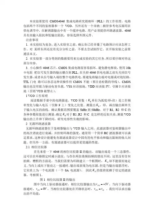
本实验要使用CMOS4046集成电路研究锁相环(PLL )的工作原理。
电路包括两个不同的鉴相器和一个VCO 。
另外还有一个齐纳二极管参考电压源用在供电调节中,在解调器输出中有一个缓冲电路。
用户必须提供环路滤波器。
4046具有高输入阻抗和低输出阻抗,容易选择外围元件。
注意事项1. 本实验较为复杂,进入实验室之前,确认你已经弄懂了电路预计应该怎样工作。
对 某样东西还没有充分分析之前,不要去尝试制作它。
在开始实验之前要通读本文。
2. 在实验第一部分得到的数据要用来完成实验的其它任务。
所以要仔细对待这部分内容。
3. 小心操作4046芯片,CMOS 集成电路很容易损坏。
避免静电释放,使用10k Ω电阻 把信号发生器的输出耦合到PLL 。
在关掉4046供电电源之前先关闭信号发生器,或者从信号输入端给整个电路供电。
要避免将输出端对电源或对地短路,TTL 门电 路可以容忍这种误操作但CMOS 不能(要注意松散的导线)。
CMOS 输出也没有能力驱动电容负载。
VSS 应该接地,VDD 应该接5V ,引脚5应该接地(否则VCO 被禁止)。
1 VCO 工作原理阅读数据手册中的电路描述。
VCO 常数(0K 单位为弧度/秒-伏)是工作频率变化与输入电压(引脚9上)变化之比值。
测量出0K ,即,画出输出频率关于输入电压的曲线。
确认数据范围要覆盖5kHz 到50kHz 。
对于R1, R2 和C 的各种参数取值进行测量,确定0K 对于R1 ,R2 和C 是怎样的近似关系。
测量VCO 输出的上升和下降时间,研究电容性负载的影响。
2 无源环路滤波器无源环路滤波器位于鉴相器输出与VCO 输入之间。
此滤波器对鉴相器输出中的高次谐波进行衰减,并控制环路的强度。
通常用一个简单RC 滤波器就可以满足要求,这种设计能避免有源滤波器设计中固有的电平移动和输出限制的恼人问题。
但另外一方面,有源滤波器可以提供更优越的性能。
2.1 相位比较器首先来看一下4046的相位比较器II 的输出。
锁相环外文参考文献译文及原文目录外文参考文献译文1锁相环 (1)1.1锁相特性 (1)1.2历史与应用 (2)1.3其它应用 (4)2光通信元件 (5)2.1光纤 (5)2.2调制器和检测器 (6)外文参考文献原文1Phase Lock Loop (9)1.1Nature of Phaselock (9)1.2History and Application (10)1.3Other Applications (13)2Optical Communication Components (14)2.1The Optical Fiber (14)2.2Modulators and Detectors (17)1锁相环1.1锁相特性锁相环包含三个组成部分:1、相位检测器(PD)。
2、环路滤波器。
3、压控振荡器(VCO),其频率由外部电压控制。
相位检测器将一个周期输入信号的相位与压控振荡器的相位进行比较。
相位检测器的输出是它两个输入信号之间相位差的度量。
差值电压由环路滤波后,再加到压控振荡器上。
压控振荡器的控制电压使频率朝着减小输入信号与本振之间相位差的方向改变。
当锁相环处于锁定状态时,控制电压使压控振荡器的频率正好等于输入信号频率的平均值。
对于输入信号的每一周期,振荡器输出也变化一周,且仅仅变化一周。
锁相环的一个显而易见的应用是自动频率控制(AFC)。
用这种方法可以获得完美的频率控制,而传统的自动频率控制技术不可避免地存在某些频率误差。
为了保持锁定环路所需的控制电压,通常要求相位检测器有一个非零的输出,所以环路是在有一些相位误差条件下工作的。
不过实际上对于一个设计良好的环路这种误差很小。
一个稍微不同的解释可提供理解环路工作原理的更好说明。
让我们假定输入信号的相位或频率上携带了信息,并且此信号不可避免地受到加性噪声地干扰。
锁相接收机的作用是重建原信号而尽可能地去除噪声。
为了重建原始信号,接收机使用一个输出频率与预计信号频率非常接近的本机振荡器。
锁相环电路原理概述By jluhong 锁相环的英文全称是Phase-Locked Loop,简称PLL。
它是由鉴相器(PD)、环路滤波器(LPF)和压控振荡器(VCO)三部分构成的一种信号相差自动调节反馈电路(环)。
PLL电路框图如下,其具体工作过程为,当输入信号Vi(t)=0时,环路滤波器的输出Vc(t)为某一固定值。
这时,压控振荡器按其固有频率fv=f0进行自由振荡。
当有频率为fi的Vi(t)输入时,Vi(t)和Vo(t)同时加到鉴相器进行鉴相。
如果二者相差不大,鉴相器输出一个与二者相位差成正比的误差电压Vd(t),再经过环路滤波器滤去Vd(t)中的高频成分,输出一个直流控制电压Vc,Vc将使压控振荡器的频率fv(和相位)发生变化,向输入信号频率fi靠拢,最后使fv= fi,环路锁定。
环路一旦进入锁定状态后,压控振荡器的输出信号与环路的输入信号(参考信号)之间只有一个固定的稳态相位差,而没有频差存在,而且当输入信号频率在捕捉带范围内变化时或相位变化时,VCO输出信号跟踪输入信号的频率和相位。
(跟踪是有条件的,即输入信号频率变化在一定范围内,否则PLL失锁)。
大家要注意,若鉴相器输入信号和VCO本振频率ωo频差很大时,鉴相器输出的差拍频率很高,则差拍频率经过环路低通滤波器被滤除了。
只有很小的分量漏加到压控振荡器的输入端。
由于控制电压太小,压控振荡器输出仍然是它的固有振荡频率ωo,整个系统输出信号基本没有发生变化,PLL失去其作用,因此要注意一个PLL电路对输入信号频率范围的限制(取决于ωo)。
鉴相器:鉴相器类型很多。
按鉴相特性分类有:正弦形鉴相器、锯齿形鉴相器、三角形鉴相器、梯形鉴相器等等;按电路性质分类有:模拟鉴相器、数字鉴相器、模拟乘法鉴相器等等。
环路滤波器可分为有源和无源二类。
压控振荡器的类别很多,常用的有LC压控振荡器,RC压控振荡器,晶体压控振荡器(VCXO)在锁相环中压控振荡器实现压控主要采用如下两种方法:直接改变决定振荡频率的振荡回路元件(如C、或R)的数值;控制多谐振荡器中定时元件的充放电流或电压。
东海科学技术学院毕业设计(论文)文献综述题目:基于VHDL的全数字锁相环的设计系:机电工程系学生姓名:专业:班级:指导教师:起止日期:文献综述一、前言随着数字技术的不断发展和计算机的普及应用,全数字锁相环ADPLL ( All Digital Phase-Locked Loop)和电子设计自动化EDA(Electronic Design Automation)技术在通信、雷达、测量、医学、工业自动化、计算机应用、仪器仪表和自动化控制等领域得到了广泛的应用。
全数字锁相环(ADPLL),是指环路部件全部数字化,采用数字鉴相器、数字环路滤波器、数控振荡器构成锁相环路,并且系统中的信号全是数字信号。
具备可靠性高、工作稳定、调节方便等优点。
它的环路带宽和中心频率编程可调,易于构建高阶锁相环,并且应用在数字系统中时,不需A/ D 及D/ A 转换[ 1]。
电子设计自动化(EDA)是一种实现电子系统或电子产品自动化设计的技术,它与电子技术、微电子技术的发展密切相关,吸收了计算机科学领域的大多数最新研究成果,以高性能的计算机作为工作平台,是20世纪90年代初从CAD(计算机辅助设计)、CAM(计算机辅助制造)、CAT(计算机辅助测试)和CAE(计算机辅助工程)的概念发展而来的。
EDA技术就是以计算机为工具,在EDA软件平台上,根据硬件描述语言HDL完成的设计文件,自动地完成逻辑编译、化简、分割、综合及优化、布局线、仿真,直至对于特定目标芯片的适配编译、逻辑映射和编程下载等工作[ 11]。
设计者的工作仅限于利用软件的方式来完成对系统硬件功能的描述,在EDA工具的帮助下和应用相应的FPG刀CPLD器件,就可以得到最后的设计结果。
尽管目标系统是硬件,但整个设计和修改过程如同完成软件设计一样方便和高效。
当然,这里的所谓EDA主要是指数字系统的自动化设计,因为这一领域的软硬件方面的技术已比较成熟,应用的普及程度也已比较大。
精心整理电子类常用缩写(英文翻译)AC(alternatingcurrent)交流(电)A/D(analogtodigital)模拟/数字转换ADC(analogtodigitalconvertor)模拟/数字转换器ADM(adaptivedeltamodulation)自适应增量调制ADPCM(adaptivedifferentialpulsecodemodulation)自适应差分脉冲编码调制ALU(arithmeticlogicunit)算术逻辑单元ASCII(AmericanstandardcodeforinformationEIA(ElectronicIndustriesAssociation)电子工业联合会EOC(endofconversion)转换结束EPROM(erasableprogrammablereadonlymemory)可擦可编程只读存储器EEPROM(electricallyEPROM)电可擦可编程只读存储器ESD(electro-staticdischarge)静电放电FET(field-effecttransistor)场效应晶体管FS(fullscale)满量程F/V(frequencytovoltageconvertor)频率/电压转换FM(frequencymodulation)调频FSK(frequencyshiftkeying)频移键控FSM(fieldstrengthmeter)场强计FST(fastswitchingshyster)快速晶闸管FT(fixedtime)固定时间FU(fuseunit)保险丝装置FWD(forward)正向的GAL(genericarraylogic)通用阵列逻辑GND(ground)接地,地线GTO(Sateturnoffthruster)门极可关断晶体管HART(highwayaddressableremotetransducer)可寻址远程传感器数据公路件)管I/I/硅开关LSB(leastsignificantbit)最低有效位LSI(1argescaleintegration)大规模集成电路M(motor)电动机MCT(MOScontrolledgyrator)场控晶闸管MIC(microphone)话筒,微音器,麦克风min(minute)分MOS(loxidesemiconductor)金属氧化物半导体MOSFET(loxidesemiconductorFET)金属氧化物半导体场效应晶体管N(negative)负NMOS(N-channelloxidesemiconductorFET)N沟道MOSFETNTC(negativetemperaturecoefficient)负温度系数OC(overcurrent)过电流OCB(overloadcircuitbreaker)过载断路器OCS(opticalcommunicationsystem)光通讯系统OR(typeoflogiccircuit)或逻辑电路OV(overvoltage)过电压P(pressure)压力FAM(pulseamplitudemodulation)脉冲幅度调制PC(pulsecode)脉冲码PCM(pulsecodemodulation)脉冲编码调制分微分(MOSFET管RAM(randomaccessmemory)随机存储器RCT(reverseconductingthyristor)逆导晶闸管REF(reference)参考,基准REV(reverse)反转R/F(radiofrequency)射频RGB(red/green/blue)红绿蓝ROM(readonlymemory)只读存储器RP(resistancepotentiometer)电位器RST(reset)复位信号RT(resistorwithinherentvariabilitydependent)热敏电阻RTD(resistancetemperaturedetector)电阻温度传感器RTL(resistortransistorlogic)电阻晶体管逻辑(电路) RV(resistorwithinherentvariabilitydependentonthe voltage)压敏电阻器SA(switchingassembly)开关组件SBS(siliconbi-directionalswitch)硅双向开关,双向硅开关SCR(siliconcontrolledrectifier)可控硅整流器SCS(safetycontrolswitch)安全控制开关SCS(siliconcontrolledswitch)可控硅开关SCS(speedcontrolsystem)速度控制系统器VCO(voltagecontrolledoscillator)压控振荡器VD(videodecoders)视频译码器VDR(voltagedependentresistor)压敏电阻VF(videofrequency)视频V/F(voltage-to-frequency)电压/频率转换V/I(voltagetocurrentconvertor)电压-电流变换器VM(voltmeter)电压表VS(vacuumswitch)电子开关VT(visualtelephone)电视电话VT(videoterminal)视频终端AC(alternatingcurrent)交流(电)A/D(analogtodigital)模拟/数字转换ADC(analogtodigitalconvertor)模拟/数字转换器ADM(adaptivedeltamodulation)自适应增量调制ADPCM(adaptivedifferentialpulsecodemodulation)自适应差分脉冲编码调制ALU(arithmeticlogicunit)算术逻辑单元ASCII(Americanstandardcodeforinformation interchange)美国信息交换标准码AV(audiovisual)声视,视听BCD(binarycodeddecimal)二进制编码的十进制数BCR(bi-directionalcontrolledrectifier)双向晶闸管只读存储器EEPROM(electricallyEPROM)电可擦可编程只读存储器ESD(electro-staticdischarge)静电放电FET(field-effecttransistor)场效应晶体管FS(fullscale)满量程F/V(frequencytovoltageconvertor)频率/电压转换FM(frequencymodulation)调频FSK(frequencyshiftkeying)频移键控FSM(fieldstrengthmeter)场强计FST(fastswitchingshyster)快速晶闸管FT(fixedtime)固定时间FU(fuseunit)保险丝装置FWD(forward)正向的GAL(genericarraylogic)通用阵列逻辑GND(ground)接地,地线GTO(Sateturnoffthruster)门极可关断晶体管HART(highwayaddressableremotetransducer)可寻址远程传感器数据公路HCMOS(highdensityCOMS)高密度互补金属氧化物半导体(器件)HF(highfrequency)高频HTL(highthresholdlogic)高阈值逻辑电路体管I/I/管MIC(microphone)话筒,微音器,麦克风min(minute)分MOS(loxidesemiconductor)金属氧化物半导体MOSFET(loxidesemiconductorFET)金属氧化物半导体场效应晶体管N(negative)负NMOS(N-channelloxidesemiconductorFET)N沟道MOSFETNTC(negativetemperaturecoefficient)负温度系数OC(overcurrent)过电流OCB(overloadcircuitbreaker)过载断路器OCS(opticalcommunicationsystem)光通讯系统OR(typeoflogiccircuit)或逻辑电路OV(overvoltage)过电压P(pressure)压力FAM(pulseamplitudemodulation)脉冲幅度调制PC(pulsecode)脉冲码PCM(pulsecodemodulation)脉冲编码调制PDM(pulsedurationmodulation)脉冲宽度调制PF(powerfactor)功率因数PFM(pulsefrequencymodulation)脉冲频率调制PG(pulsegenerator)脉冲发生器MOSFET管R/F(radiofrequency)射频RGB(red/green/blue)红绿蓝ROM(readonlymemory)只读存储器RP(resistancepotentiometer)电位器RST(reset)复位信号RT(resistorwithinherentvariabilitydependent)热敏电阻RTD(resistancetemperaturedetector)电阻温度传感器RTL(resistortransistorlogic)电阻晶体管逻辑(电路) RV(resistorwithinherentvariabilitydependentonthe voltage)压敏电阻器SA(switchingassembly)开关组件SBS(siliconbi-directionalswitch)硅双向开关,双向硅开关SCR(siliconcontrolledrectifier)可控硅整流器SCS(safetycontrolswitch)安全控制开关SCS(siliconcontrolledswitch)可控硅开关SCS(speedcontrolsystem)速度控制系统SCS(supplycontrolsystem)电源控制系统SG(sparkgap)放电器SIT(staSITH(staticinductionthyristor)静电感应晶闸管抗器V/F(voltage-to-frequency)电压/频率转换V/I(voltagetocurrentconvertor)电压-电流变换器VM(voltmeter)电压表VS(vacuumswitch)电子开关VT(visualtelephone)电视电话VT(videoterminal)视频终端。
锁相技术译文翻译英文原文:An On-Chip All-Digital Measurement Circuit to Characterize Phase-Locked Loop Response in 45-nm SOI译文:45纳米SOI全数字片上测量电路表征锁相环响应特性年级专业:姓名:学号:2013 年 6 月 2 日英文中文An On-Chip All-Digital Measurement Circuit to Characterize Phase-Locked Loop Response in 45-nm SOIAbstract—An all-digital measurement Circuit , built in 45-nm SOI-CMOS enabl es on-chip characterization of phase-loc ked loop (PLL) response to a self-induce d phase step.This technique allows estimationof PLL closed-loop bandwidth and jitterpeaking. The circuit canbe used to plot step-response vs.time, measure static phase error,and observe phase-lock status. INTRODUCTIONMany applications such as PCI Express ? require a PLL to produce alow-jitter cl ock at a given frequency while meeting stringent bandwidth and jitter peaking r 45纳米SOI全数字片上测量电路表征锁相环响应特性摘要---建立在45纳米的SOI-CMOS上一个全数字测量电路,它能够表征PLL对自诱导相步进的响应这项技术允许对PLL闭环带宽和抖动峰值的估计。
电子专业词汇的中英文对照电路的基本概念及定律电源source电压源voltage source电流源current source理想电压源ideal voltage source理想电流源ideal current source伏安特性volt-ampere characteristic 电动势electromotive force电压voltage电流current电位potential电位差potential difference欧姆Ohm伏特Volt安培Ampere瓦特Watt焦耳Joule电路circuit电路元件circuit element电阻resistance电阻器resistor电感inductance电感器inductor电容capacitance电容器capacitor电路模型circuit model参考方向reference direction参考电位reference potential欧姆定律Ohm’s law基尔霍夫定律Kirchhoff’s law基尔霍夫电压定律Kirchhoff’s voltage law(KVL)基尔霍夫电流定律Kirchhoff’s current law(KCL)结点node支路branch回路loop网孔mesh支路电流法branch current analysis网孔电流法mesh current analysis结点电位法node voltage analysis电源变换source transformations叠加原理superposition theorem网络network无源二端网络passive two-terminal network有源二端网络active two-terminal network戴维宁定理Thevenin’s theorem诺顿定理Norton’s theorem开路(断路)open circuit短路short circuit开路电压open-circuit voltage短路电流short-circuit current交流电路直流电路direct current circuit (dc)交流电路alternating current circuit (ac)正弦交流电路sinusoidal a-c circuit平均值average value有效值effective value均方根值root-mean-squire value (rms) 瞬时值instantaneous value电抗reactance感抗inductive reactance容抗capacitive reactance法拉Farad亨利Henry阻抗impedance复数阻抗complex impedance相位phase初相位initial phase相位差phase difference相位领先phase lead相位落后phase lag倒相,反相phase inversion频率frequency角频率angular frequency赫兹Hertz相量phasor相量图phasor diagram有功功率active power无功功率reactive power视在功率apparent power功率因数power factor功率因数补偿power-factor compensation串联谐振series resonance并联谐振parallel resonance谐振频率resonance frequency频率特性frequency characteristic幅频特性amplitude-frequency response characteristic相频特性phase-frequency response characteristic截止频率cutoff frequency品质因数quality factor 通频带pass-band带宽bandwidth (BW)滤波器filter一阶滤波器first-order filter二阶滤波器second-order filter低通滤波器low-pass filter高通滤波器high-pass filter带通滤波器band-pass filter带阻滤波器band-stop filter转移函数transfer function波特图Bode diagram傅立叶级数Fourier series三相电路三相电路three-phase circuit三相电源three-phase source对称三相电源symmetrical three-phase source对称三相负载symmetrical three-phase load相电压phase voltage相电流phase current线电压line voltage线电流line current三相三线制three-phase three-wire system三相四线制three-phase four-wire system三相功率three-phase power星形连接star connection(Y-connection) 三角形连接triangular connection(D- connection ,delta connection)中线neutral line电路的暂态过程分析暂态transient state稳态steady state暂态过程,暂态响应transient response 换路定理low of switch一阶电路first-order circuit三要素法three-factor method时间常数time constant积分电路integrating circuit微分电路differentiating circuit磁路与变压器磁场magnetic field磁通flux磁路magnetic circuit磁感应强度flux density磁通势magnetomotive force磁阻reluctance电动机直流电动机dc motor交流电动机ac motor异步电动机asynchronous motor同步电动机synchronous motor三相异步电动机three-phase asynchronous motor单相异步电动机single-phase asynchronous motor旋转磁场rotating magnetic field定子stator转子rotor转差率slip起动电流starting current起动转矩starting torque额定电压rated voltage 额定电流rated current额定功率rated power机械特性mechanical characteristic继电器-接触器控制按钮button熔断器fuse开关switch行程开关travel switch继电器relay接触器contactor常开(动合)触点normally open contact 常闭(动断)触点normally closed contact 时间继电器time relay热继电器thermal overload relay中间继电器intermediate relay可编程控制器(PLC)可编程控制器programmable logic controller语句表statement list梯形图ladder diagram半导体器件本征半导体intrinsic semiconductor掺杂半导体doped semiconductorP型半导体P-type semiconductorN型半导体N--type semiconductor自由电子free electron空穴hole载流子carriersPN结PN junction扩散diffusion漂移drift二极管diode硅二极管silicon diode锗二极管germanium diode阳极anode阴极cathode发光二极管light-emitting diode (LED) 光电二极管photodiode稳压二极管Zener diode晶体管(三极管)transistorPNP型晶体管PNP transistorNPN型晶体管NPN transistor发射极emitter集电极collector基极base电流放大系数current amplification coefficient场效应管field-effect transistor (FET) P沟道p-channelN沟道n-channel结型场效应管junction FET(JFET)金属氧化物半导体metal-oxide semiconductor (MOS)耗尽型MOS场效应管depletion mode MOSFET(D-MOSFET)增强型MOS场效应管enhancement mode MOSFET(E-MOSFET)源极source栅极grid漏极drain跨导transconductance夹断电压pinch-off voltage热敏电阻thermistor开路open短路shorted 基本放大器放大器amplifier正向偏置forward bias反向偏置backward bias静态工作点quiescent point (Q-point)等效电路equivalent circuit电压放大倍数voltage gain总的电压放大倍数overall voltage gain 饱和saturation截止cut-off放大区amplifier region饱和区saturation region截止区cut-off region失真distortion饱和失真saturation distortion截止失真cut-off distortion零点漂移zero drift正反馈positive feedback负反馈negative feedback串联负反馈series negative feedback并联负反馈parallel negative feedback 共射极放大器common-emitter amplifier 射极跟随器emitter-follower共源极放大器common-source amplifier 共漏极放大器common-drain amplifier 多级放大器multistage amplifier阻容耦合放大器resistance-capacitance coupled amplifier直接耦合放大器direct- coupled amplifier输入电阻input resistance输出电阻output resistance负载电阻load resistance动态电阻dynamic resistance负载电流load current旁路电容bypass capacitor耦合电容coupled capacitor直流通路direct current path交流通路alternating current path直流分量direct current component交流分量alternating current component 变阻器(电位器)rheostat电阻(器)resistor电阻(值)resistance电容(器)capacitor电容(量)capacitance电感(器,线圈)inductor电感(量),感应系数inductance正弦电压sinusoidal voltage集成运算放大器及应用差动放大器differential amplifier运算放大器operationalamplifier(op-amp)失调电压offset voltage失调电流offset current共模信号common-mode signal差模信号different-mode signal共模抑制比common-mode rejection ratio (CMRR)积分电路integrator(circuit)微分电路differentiator(circuit)有源滤波器active filter低通滤波器low-pass filter高通滤波器high-pass filter带通滤波器band-pass filter带阻滤波器band-stop filter 波特沃斯滤波器Butterworth filter切比雪夫滤波器Chebyshev filter贝塞尔滤波器Bessel filter截止频率cut-off frequency上限截止频率upper cut-off frequency下限截止频率lower cut-off frequency中心频率center frequency带宽Bandwidth开环增益open-loop gain闭环增益closed-loop gain共模增益common-mode gain输入阻抗input impedance电压跟随器voltage-follower电压源voltage source电流源current source单位增益带宽unity-gain bandwidth频率响应frequency response频响特性(曲线)response characteristic 波特图the Bode plot稳定性stability补偿compensation比较器comparator迟滞比较器hysteresis comparator阶跃输入电压step input voltage仪表放大器instrumentation amplifier隔离放大器isolation amplifier对数放大器log amplifier反对数放大器antilog amplifier反馈通道feedback path反向漏电流reverse leakage current相位phase相移phase shift锁相环phase-locked loop(PLL)锁相环相位监测器PLL phase detector 和频sum frequency差频difference frequency波形发生电路振荡器oscillatorRC振荡器RC oscillatorLC振荡器LC oscillator正弦波振荡器sinusoidal oscillator三角波发生器triangular wave generator 方波发生器square wave generator幅度magnitude电平level饱和输出电平(电压)saturated output level功率放大器功率放大器power amplifier交越失真cross-over distortion甲类功率放大器class A power amplifier 乙类推挽功率放大器class B push-pull power amplifierOTL功率放大器output transformerless power amplifierOCL功率放大器output capacitorless power amplifier直流稳压电源半波整流full-wave rectifier全波整流half-wave rectifier电感滤波器inductor filter电容滤波器capacitor filter串联型稳压电源series (voltage) regulator开关型稳压电源switching (voltage) regulator集成稳压器IC (voltage) regulator 晶闸管及可控整流电路晶闸管thyristor单结晶体管unijunction transistor(UJT)可控整流controlled rectifier可控硅silicon-controlled rectifier峰点peak point谷点valley point控制角controlling angle导通角turn-on angle门电路与逻辑代数二进制binary二进制数binary number十进制decimal十六进制hexadecimal二-十进制binary coded decimal (BCD)门电路gate三态门tri-state gate与门AND gate或门OR gate非门NOT gate与非门NAND gate或非门NOR gate异或门exclusive-OR gate反相器inverter布尔代数Boolean algebra真值表truth table卡诺图the Karnaugh map逻辑函数logic function逻辑表达式logic expression组合逻辑电路组合逻辑电路combination logic circuit 译码器decoder编码器coder比较器comparator半加器half-adder全加器full-adder七段显示器seven-segment display 时序逻辑电路时序逻辑电路sequential logic circuit R-S 触发器R-S flip-flopD触发器D flip-flopJ-K触发器J-K flip-flop主从型触发器master-slave flip-flop 置位set复位reset直接置位端direct-set terminal直接复位端direct-reset terminal寄存器register移位寄存器shift register双向移位寄存器bidirectional shift register计数器counter同步计数器synchronous counter异步计数器asynchronous counter 加法计数器adding counter减法计数器subtracting counter定时器timer清除(清0)clear载入load时钟脉冲clock pulse触发脉冲trigger pulse上升沿positive edge下降沿negative edge 时序图timing diagram波形图waveform脉冲波形的产生与整形单稳态触发器monostable flip-flop双稳态触发器bistable flip-flop无稳态振荡器astable oscillator晶体crystal555定时器555 timer模拟信号与数字信号的相互转换模拟信号analog signal数字信号digital signalAD转换器analog -digital converter (ADC) DA转换器digital-analog converter (DAC)半导体存储器只读存储器read-only memory(ROM)随机存取存储器random-access memory(RAM)可编程ROM programmable ROM (PROM)Linear Control System(线性系统), Single Input Single Output(单输入单输出), Laplace Transform(拉普拉斯变换), Differential Equations(微分方程), Transfer Functions(传递函数), Models of System(系统模型), Block Diagrams(方框图), Mason’s Gain Formula(梅森公式), First-order System(一阶系统), Second-order System(二阶系统), Higher-order System(高阶系统), Close-loop Control System(闭环控制系统), Stability(稳定性), Transient Response(瞬态响应), Routh-Hurwitz Stability Criterion(劳斯判据), Steady-state Accuracy(稳态精度), Root-locus(根轨迹), Root-locus Principles(根轨迹基本规则), Frequency Responses(频率响应), Bode Diagrams(波特图), Nyquist Criterion(奈氏判据), Relative Stability(相对稳定性).。
锁相技术译文翻译英文原名:High Speed Digital Hybrid PLL Frequency Synthesizer译文:高速数字混合锁相环频率合成器年纪专业:08级通信工程班姓名:学号:2011年 5月2日To get the high-speed, it is necessary to prepare the precise synchronization of the complicated design.In 2001, H. G. Ryu proposed a simplified structure of the DDFS (direct digital frequency synthesizer)-driven PLL for the high switching speed [2].However, there is a problem that the speed of the whole system is limited by PLL.Y. Fouzar proposed a PLL frequency synthesizer of dual loop configuration using frequency-to-voltage converter (FVC) [3].It has a fast switching speed by the PD (phase detector), FVC using output signal of VCO and the proposed coarse tuning controller.However, H/W complexity is increased for the high switching speed.Also, it shows the fast switching characteristic only when the FVC works well.Another method is pre-tuning one which is called DH-PLL in this study [4].It has very high speed switching property, but H/W complexity and power consumption are increased due to digital look-up table (DLT) which is usually implemented by the ROM including the transfer characteristic ofVCO(voltage controlled oscillator).For this reason, this paper proposes a timing synchronization circuit for the rapid frequency synthesis and a very simple DLT replacement digital logic block instead of the complex ROM type DLT for high speed switching and low power consumption. Also, the requisite condition is solved in the proposed method. The fast switching operation at every the frequency synthesis process is verified by the computer circuit simulation.II.DH-PLL synthesizerAs shown in Fig.1, the open-loop synthesizer is a direct frequency synthesis type that VCO 要得到高运行速度,事先做好复杂设计的精确同步是必要的。
本科生毕业设计 (论文)外文翻译原文标题Designing,Simulating,and Testing an AnalogPhase-Locked LoopPhase-Locked Loop in a Digital Environment译文标题在数码环境下设计、模拟和测试一个模拟锁相环作者所在系别电子工程系作者所在专业自动化作者所在班级B06223作者姓名司洪珲作者学号20064022318指导教师姓名齐建玲指导教师职称副教授完成时间2009 年12 月北华航天工业学院教务处制译文标题在数码环境下设计,模拟和测试一个模拟锁相环原文标题Designing,Simulating,and Testing an Analog Phase-Locked Loop in aDigital Environment作者Thomas J. ThatcherMichael M. OshimaCindy Botelho译名托马斯.撒切尔罗切斯特辛迪博特略国籍美国美国美国原文出处April 1997 Hewlett-Packard Journal 6在数码环境下设计,模拟和测试一个模拟锁相环唐静文,中国香港罗切斯特,美国设计用在几项惠普ASIC上的锁相环时,现有阶段的数字部分锁相环被转移成一个VHDL描述与合成的行为。
在模拟部分写出一种行为模型,使ASIC设计师模拟运行系统。
开发出了一种新的非常有效的,用于筛选出在原来的设计过滤过程中的缺陷的泄漏试验。
本文介绍了设计和集成几个正在当前应用专用集成电路的锁相环的一个阶段过程。
该设计是基于锁相环的ASIC上一个循环,但有一些改进。
首先,该阶段的数字部分锁相环被转移到了一种VHDL描述与合成的行为。
在编写代码时,可重用性是一个大的考虑。
VHDL代码的便携性使我们能在很短的时间内设计几种锁相环。
第二,写一个行为模型的模拟部分,这样使ASIC设计师模拟运行系统。
在全数字化设计环境下,对于设计师模拟锁相环提出了若干挑战。
第十五篇锁相环PLL及APBDIV关于锁相环的内容早就应该涉及,因为之前的定时器计数周期,和之后的串口波特率、AD转换频率等都与此相关。
锁相环的英文名为:Phase Locked Loop,其实它的作用就是一个倍频器,它把外部晶振频率(Fosc)加倍后得到系统时钟(Fcclk)给CPU使用,即:Fcclk=Fosc*M,这个M值是可设定的,它就是寄存器PLLCFG的低五位决定,但M值不能随意设定,比如LPC2103的Fcclk不能超过60MHz。
还有一个频率叫Fcco,它是PLL内部的CCO(电流控制振荡器current controlled oscillator)的频率,Fcco=Fcclk*2*P,P由PLLCFG[6:5]决定,我们不要对它有过多注意力,因为外围电路和Fcco无关,CCO只是为了保证PLL正常工作且在其内部的一个部件(想知道具体机制查相关资料),我们唯一要做的是使Fcco 处于正常的范围(LPC2000系列ARM的CCO要求工作在156~320MHz)之内就行了。
还有,Fpclk是我们必须注意的,芯片外设工作于PCLK(APB clock),(APB 和AHB是外围电路中的两种总线,AHB速度快,用于VIC;APB用于其它外设:定时器、串口等),PCLK由FCCLK分频得到(通过APB分频器),分频值由寄存器APBDIV[1:0]决定,其它位保留。
上述频率的关系如下图:下面具体说明程序中应该如何设置这些频率值:首先说一下这些倍数的配置寄存器:所谓M由PLLCFG[4:0]决定,并不是二者相等,而是M=PLLCFG[4:0]+1;还有P=2^PLLCFG[6:5](2的n次幂);还有:APBDIV[1:0]=00,Fcclk/Fpclk=1/4;APBDIV[1:0]=01,Fcclk/Fpclk=1;APBDIV[1:0]=10,Fcclk/Fpclk=1/2;APBDIV[1:0]=11,保留。
锁相环的研究与设计——用于DSP芯片时钟发生器
的开题报告
一、研究背景
随着现代数字信号处理技术的日益成熟,数字信号处理(DSP)芯片在通信、音视频处理、图像处理等领域得到了广泛应用。
因为DSP芯片需要精确的时钟信号来同步各个模块之间的数据传输,常用的时钟发生器是基于晶振的,然而晶振的频率稳定性和精度难以满足高精度时钟信号的要求。
锁相环(PLL)是一种常用的时钟发生器,用于将一个参考时钟信号锁定到设定频率的输出时钟信号。
锁相环可以提供相对于晶振更高的频率稳定性和精度,适用于DSP芯片的时钟信号发生器。
二、研究内容
本论文将重点研究锁相环的理论原理与设计方法,并将其应用于DSP芯片的时钟发生器中。
主要研究内容包括:
1. 锁相环的基本结构和原理。
重点分析锁相环中的相位检测器、环路滤波器和控制电路等核心组成部分,并探讨其作用和影响因素。
2. 锁相环的设计方法。
基于理论分析和电路实现,设计一种高性能的锁相环,包括参数选取、电路布局和仿真验证等环节。
3. DSP芯片时钟发生器的整体设计。
将锁相环与其他电路模块相结合,构建一个完整的DSP芯片时钟发生器,并对其进行整体性能测试与验证。
三、研究意义
本论文的研究结果可以为DSP芯片时钟发生器的设计与制造提供参考,并为相关领域的进一步研究提供理论基础和实践经验。
同时,本研究探讨的锁相环设计方法可适用于其他电子设备中时钟发生器的设计与制造,具有一定的普适性和推广价值。
外文资料Phase-locked loop Technology :A phase-locked loop or phase lock loop (PLL) is a control system that generates a signal that has a fixed relation to the phase of a "reference" signal. A phase-locked loop circuit responds to both the frequency and the phase of the input signals, automatically raising or lowering the frequency of a controlled oscillator until it is matched to the reference in both frequency and phase. A phase-locked loop is an example of a control system using negative feedback. In the order of the PLL is the way of made the frequency stability in the send up wireless,include VCO and PLL integrated circuits,VCO send up a signal,some of the signal is output,and the other through the frequency division with PLL integrated circuits generate the local signal making compared.In the order to remain the same,it’s must be remain the phase displacement same.If the phase displacement have some changes,the output of the PLL integrated circuits have some changes too,to controlle VCO until phase diffe rence to restore,make both cotrolled oscillator’s frequency and phase with input signal which is close-loop electronic circuit keep firm relationship.Phase-locked loops are widely used in radio, telecommunications, computers and other electronic applications. They may generate stable frequencies, recover a signal from a noisy communication channel, or distribute clock timing pulses in digital logic designs such as microprocessors. Since a single integrated circuit can provide a complete phase-locked-loop building block, the technique is widely used in modern electronic devices, with output frequencies from a fraction of a cycle per second up to many gigahertz.Earliest research towards what became known as the phase-locked loop goes back to 1932, when British researchers developed an alternative to Edwin Armstrong's superheterodyne receiver, the Homodyne. In the homodyne or synchrodyne system, a local oscillator was tuned to the desired input frequency and multiplied with the input signal. The resulting output signal included the original audio modulation information.The intent was to develop an alternative receiver circuit that required fewer tuned circuits than the superheterodyne receiver. Since the local oscillator would rapidly drift in frequency, an automatic correction signal was applied to the oscillator, maintaining it in the same phase and frequency as the desired signal. The technique was described in 1932, in a paper by H.de Bellescise, in the French journal Onde Electrique.In analog television receivers since at least the late 1930s, phase-locked-loop horizontal and vertical sweep circuits are locked to synchronization pulses in the broadcast signal. When Signetics introduced a line of monolithic integrated circuits that were complete phase-locked loop systems on a chip in 1969, applications for the technique multiplied. A few years later RCA introduced the "CD4046" CMOS Micropower Phase-Locked Loop, which became a popular integrated circuit. Applications:Phase-locked loops are widely used for synchronization purposes; in space communications for coherent carrier tracking and threshold extension, bit synchronization, and symbol synchronization. Phase-locked loops can also be used to demodulate frequency-modulated signals. In radio transmitters, a PLL is used to synthesize new frequencies which are a multiple of a reference frequency, with the same stability as the reference frequency.Clock recovery :Some data streams, especially high-speed serial data streams (such as the raw stream of data from the magnetic head of a disk drive), are sent without an accompanying clock. The receiver generates a clock from an approximate frequency reference, and then phase-aligns to the transitions in the data stream with a PLL. This process is referred to as clock recovery. In order for this scheme to work, the data stream must have a transition frequently enough to correct any drift in the PLL's oscillator. Typically, some sort of redundant encoding is used; 8B10B is very common.Deskewing :If a clock is sent in parallel with data, that clock can be used to sample the data.Because the clock must be received and amplified before it can drive the flip-flops which sample the data, there will be a finite, and process-, temperature-, and voltage-dependent delay between the detected clock edge and the received data window. This delay limits the frequency at which data can be sent. One way of eliminating this delay is to include a deskew PLL on the receive side, so that the clock at each data flip-flop is phase-matched to the received clock. In that type of application, a special form of a PLL called a Delay-Locked Loop (DLL) is frequently used.Clock generation:Many electronic systems include processors of various sorts that operate at hundreds of megahertz. Typically, the clocks supplied to these processors come from clock generator PLLs, which multiply a lower-frequency reference clock (usually 50 or 100 MHz) up to the operating frequency of the processor. The multiplication factor can be quite large in cases where the operating frequency is multiple gigahertz and the reference crystal is just tens or hundreds of megahertz.Spread spectrum:All electronic systems emit some unwanted radio frequency energy. Various regulatory agencies (such as the FCC in the United States) put limits on the emitted energy and any interference caused by it. The emitted noise generally appears at sharp spectral peaks (usually at the operating frequency of the device, and a few harmonics).A system designer can use a spread-spectrum PLL to reduce interference with high-Q receivers by spreading the energy over a larger portion of the spectrum. For example, by changing the operating frequency up and down by a small amount (about 1%), a device running at hundreds of megahertz can spread its interference evenly over a few megahertz of spectrum, which drastically reduces the amount of noise seen by FM receivers which have a bandwidth of tens of kilohertz.中文翻译锁相环技术:锁相环或锁相回路(PLL)是一个信号控制系统,即用来锁定一系列的“参考”信号。
锁相环的英文全称是Phase-Locked Loop,简称PLL。
锁相环电路是一种反馈电路,其作用是使得电路上的时钟和某一外部时钟的相位同步。
因锁相环可以实现输出信号频率对输入信号频率的自动跟踪,所以锁相环通常用于闭环跟踪电路。
锁相环在工作的过程中,当输出信号的频率与输入信号的频率相等时,输出电压与输入电压保持固定的相位差值,即输出电压与输入电压的相位被锁住,这就是锁相环名称的由来。
锁相环的工作原理:1. 压控振荡器的输出经过采集并分频;2. 和基准信号同时输入鉴相器; 3. 鉴相器通过比较上述两个信号的频率差,然后输出一个直流脉冲电压;4. 控制VCO,使它的频率改变;5. 这样经过一个很短的时间,VCO 的输出就会稳定于某一期望值。
锁相环路在锁定后,不仅能使输出信号频率与输入信号频率严格同步,而且还具有频率跟踪特性,所以它在电子技术的各个领域中都有着广泛的应用。
PLL实际上是一负反馈系统,只要输入信号在正常范围内,输出信号在“一定时间内”都能跟上。
输入信号发生变化后,输出信号跟踪输入信号的过程称之为捕获;输出信号跟踪完毕时称之为锁定;输入信号变化过快导致输出信号无法跟踪时称为失锁。
在数据采集系统中,锁相环是一种非常有用的同步技术,因为通过锁相环,可以使得不同的数据采集板卡共享同一个采样时钟。
因此,所有板卡上各自的本地80MHz 和20MHz时基的相位都是同步的,从而采样时钟也是同步的。
因为每块板卡的采样时钟都是同步的,所以都能严格地在同一时刻进行数据采集。
PLL通常由鉴相器(PD)、环路滤波器(LF)和压控振荡器(VCO)三部分组成,PLL组成的原理框图如图1所示。
如图2所示,PLL频率合成器是由参考频率源、参考分频器、相位比较器、环路滤波器、压控振荡器、可变分频器构成。
参考分频器对参考频率源进行分频,输出信号作为相位比较器参考信号。
可变分频器对压控振荡器的输出信号进行分频,分频之后返回到相位比较器输入端与参考信号进行比较。
目录1. 锁相环技术的产生背景 (1)2. 锁相环概述 (2)2.1 锁相环定义 (2)2.2 锁相环的组成部分 (2)2.3 锁相环的分类与特点 (3)2.4 锁相环的优点 (4)3. 模拟锁相环与数字锁相环 (4)3.1 模拟锁相环 (4)3.1.1 模拟锁相环的基本结构 (4)3.1.2 模拟锁相环的工作原理 (5)3.2 全数字锁相环 (6)3.2.1 全数字锁相环的基本结构 (6)3.2.2 全数字锁相环的工作原理 (7)4. 锁相环技术的应用及发展 (8)4.1 锁相环的应用 (8)4.2 锁相环的发展 (8)1.锁相环技术的产生背景锁相环路是一种反馈电路,锁相环的英文全称是Phase-Locked Loop,简称PLL,是指一种电路或者模块,它用于在通信的接收机中,其作用是对接收到的信号进行处理,并从其中提取某个时钟的相位信息。
或者说,对于接收到的信号,仿制一个时钟信号,使得这两个信号从某种角度来看是同步的(或者说,相干的)。
其作用是使得电路上的时钟和某一外部时钟的相位同步。
因锁相环可以实现输出信号频率对输入信号频率的自动跟踪,所以锁相环通常用于闭环跟踪电路。
锁相环在工作的过程中,当输出信号的频率与输入信号的频率相等时,输出电压与输入电压保持固定的相位差值,即输出电压与输入电压的相位被锁住,这就是锁相环名称的由来。
锁相环路诞生于20世纪30年代。
在40年代开始在电视接收技术中得到广泛应用。
此后空间技术的发展又极大的促进了锁相技术的发展,现已广泛应用于电子技术的各个领域。
随着数字电路技术的发展,数字锁相环在调制解调、频率合成、FM 立体声解码、彩色副载波同步、图象处理等各个方面得到了广泛的应用。
数字锁相环不仅吸收了数字电路可靠性高、体积小、价格低等优点,还解决了模拟锁相环的直流零点漂移、器件饱和及易受电源和环境温度变化等缺点,此外还具有对离散样值的实时处理能力,已成为锁相技术发展的方向。
锁相技术译文翻译英文原名:High Speed Digital Hybrid PLL Frequency Synthesizer译文:高速数字混合锁相环频率合成器年纪专业:08级通信工程班姓名:学号:2011年 5月2日To get the high-speed, it is necessary to prepare the precise synchronization of the complicated design.In 2001, H. G. Ryu proposed a simplified structure of the DDFS (direct digital frequency synthesizer)-driven PLL for the high switching speed [2].However, there is a problem that the speed of the whole system is limited by PLL.Y. Fouzar proposed a PLL frequency synthesizer of dual loop configuration using frequency-to-voltage converter (FVC) [3].It has a fast switching speed by the PD (phase detector), FVC using output signal of VCO and the proposed coarse tuning controller.However, H/W complexity is increased for the high switching speed.Also, it shows the fast switching characteristic only when the FVC works well.Another method is pre-tuning one which is called DH-PLL in this study [4].It has very high speed switching property, but H/W complexity and power consumption are increased due to digital look-up table (DLT) which is usually implemented by the ROM including the transfer characteristic ofVCO(voltage controlled oscillator).For this reason, this paper proposes a timing synchronization circuit for the rapid frequency synthesis and a very simple DLT replacement digital logic block instead of the complex ROM type DLT for high speed switching and low power consumption. Also, the requisite condition is solved in the proposed method. The fast switching operation at every the frequency synthesis process is verified by the computer circuit simulation.II.DH-PLL synthesizerAs shown in Fig.1, the open-loop synthesizer is a direct frequency synthesis type that VCO 要得到高运行速度,事先做好复杂设计的精确同步是必要的。
2001年,H.G.Ryu提出了一种简化结构的直接数字频率合成器(DDFS)驱动的高转换速度锁相环【2】。
但是,有一个问题,整个系统的速度是受锁相环限制的。
Y.Fouzar提出了一种使用频率—电压转换器(FVC)具有双重回路结构的锁相环频率合成器【3】。
因为鉴相器(PD), FVC利用了压控振荡器的输出信号和我们提出的粗调控制器,所以它具有快速切换速度。
但是,因为有高速系统转换速度使得H / W的复杂性增加了。
另外,结果表明只有FVC工作状态良好时系统才有较高切换速度。
另一种方法是做预先调整也就是本项研究中的DH-PLL 【4】。
它具有高速切换的特性,但是因为数字查找表(DLT)的原因,H / W复杂度和功耗明显增大了,因为DLT 经常被ROM执行,DLT中包含压控振荡器(VCO)的传输特性。
介于以上原因, 为得到较高切换速度和低功耗,本文提出了一种新的快速定时同步频率合成电路,用一个非常简单的DLT替代数字逻辑块,而不用复杂的ROM型(DLT)。
同时,在该方法中所需必要条件也解决了,频率合成过程的高切换速度在计算机电路仿真中已经得到验证了。
2.DH-PLL合成器图1中所示的开环频率合成技术是一种直接频率合成方式,在频率控generates the desired output by the FCW (frequency control word) input from the D/A converter.The digital frequency word which is produced from the ROM type DLT (digital look-up table) containing the VCO transfer characteristic goes into D/A converter that generates the DC value corresponding to the desired VCO frequency.Fig. 1. Open-loop frequency synthesizer. The DC value is already found by the voltage-frequency characteristics of VCO. This open-loop frequency synthesizer has fast switching speed.However, it has the big problems of stability and sensitivity due to the inherent properties of the open loop structure.Therefore, this synthesizer type is not so attractive that this synthesizer is not widely used.Fig. 2. Closed-loop PLL frequency synthesizer. 制字(FCW)控制下VCO产生了期望的输出,VCO输入来自于D / A转换器。
该数字频率控制字是由ROM类型的包含压控振荡器传输特性的数字查找表(DLT)产生的,进入D / A转换器,生成与预期的压控振荡器的频率值相对应的直流电压。
图1 .开环频率合成器。
直流电压值已经根据VCO的电压—频率特性建立了。
该开环频率合成器具有高切换速度。
但是, 由于开环结构的固有特性,该频率合成器在稳定性和灵敏度方面还有比较大的问题。
因此,这种合成器类型缺乏吸引力,该合成器没有广泛应用。
图 2.闭合回路PLL 频率合成器。
In Fig. 2, FCW (frequency control word) is the division ratio command for frequency synthesis.This structure is very popular and excellent in the aspects of the stability, variety and flexibility.Also, the spurious noise is smaller than other frequency synthesizer.It takes the longer acquisition time to jump into a new frequency so that the switching speed is low.The switching time gets longer as the generation frequency spacing is increased. DH-PLL frequency synthesizer is shown in Fig.3.Fig.3.DH-PLL using DLT (digital look-up table). The open-loop structure of the DLT and DAC is combined into the conventional PLL closed-loop structure.In the conventional PLL, the output voltage of LF is fed to the VCO.On the contrary, sum of DAC output voltage and the LF output voltage drives the VCO whenever FCW is changed.Therefore, unlike conventional PLL, DAC outputs the steady state driving voltage at every new FCW change times so that high speed frequency switching may be possible. However, the DH-PLL has a serious problem of the phase change at every new frequency synthesis.As shown in Fig. 4, the overshoot and the settling time have a trade-off relationship 在图2中,频率控制字(FCW)为频率合成分频比控制指令。