
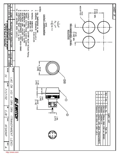
LASOAV11HGRNGRN;中文规格书,Datasheet资料
- 格式:pdf
- 大小:49.48 KB
- 文档页数:2

February 2008 Rev 61/31VN5050AJ-ESingle channel high side driver with analog current sense for automotive applicationsFeatures■General features–Inrush current active management by power limitation–Very low stand-by current – 3.0V CMOS compatible input–Optimized electromagnetic emission –Very low electromagnetic susceptibility –In compliance with the 2002/95/EC European directive ■Diagnostic functions–Proportional load current sense–High current sense precision for wide range currents–Current sense disable–Thermal shutdown indication –Very low current sense leakage■Protection–Undervoltage shut-down –Overvoltage clamp –Load current limitation–Self limiting of fast thermal transients–Protection against loss of ground and loss of V CC–Thermal shut down–Reverse battery protection ( see Application schematic )–Electrostatic discharge protectionApplication■All types of resistive, inductive and capacitive loads■Suitable as LED driverDescriptionThe VN5050AJ-E is a monolithic device made using STMicroelectronics VIPower technology. It is intended for driving resistive or inductive loads with one side connected to ground. Active V CC pin voltage clamp protects the device against low energy spikes (see ISO7637 transient compatibility table).This device integrates an analog current sense which delivers a current proportional to the load current (according to a known ratio) when CS_DIS is driven low or left open.When CS_DIS is driven high, the CURRENT SENSE pin is in a high impedance condition.Output current limitation protects the device in overload condition. In case of long overloadduration, the device limits the dissipated power to safe level up to thermal shut-down intervention. Thermal shut-down with automatic restart allows the device to recover normal operation as soon as fault condition disappears.Max supply voltage V CC 41 V Operating voltage range V CC 4.5 to 36V Max On-State resistance R ON 50 m ΩCurrent limitation (typ)I LIMH 16.5 A Off state supply currentI S2 µAPowerSSO-12Table 1.Device summaryPackage Order codesTubeTape and Reel PowerSSO-12VN5050AJ-EVN5050AJTR-EContents VN5050AJ-EContents1Block diagram and pin description . . . . . . . . . . . . . . . . . . . . . . . . . . . . . 52Electrical specifications . . . . . . . . . . . . . . . . . . . . . . . . . . . . . . . . . . . . . . 72.1Absolute maximum ratings . . . . . . . . . . . . . . . . . . . . . . . . . . . . . . . . . . . . . 72.2Thermal data . . . . . . . . . . . . . . . . . . . . . . . . . . . . . . . . . . . . . . . . . . . . . . . 82.3Electrical characteristics . . . . . . . . . . . . . . . . . . . . . . . . . . . . . . . . . . . . . . . 92.4Electrical characteristics curves . . . . . . . . . . . . . . . . . . . . . . . . . . . . . . . . 183Application information . . . . . . . . . . . . . . . . . . . . . . . . . . . . . . . . . . . . . 213.1GND protection network against reverse battery . . . . . . . . . . . . . . . . . . . 213.1.1Solution 1: resistor in the ground line (RGND only) . . . . . . . . . . . . . . . . 213.1.2Solution 2: diode (D GND) in the ground line . . . . . . . . . . . . . . . . . . . . . . 223.2Load dump protection . . . . . . . . . . . . . . . . . . . . . . . . . . . . . . . . . . . . . . . . 223.3MCU I/O protection . . . . . . . . . . . . . . . . . . . . . . . . . . . . . . . . . . . . . . . . . . 223.4Maximum demagnetization energy (VCC = 13.5V) . . . . . . . . . . . . . . . . . 234Package and PCB thermal data . . . . . . . . . . . . . . . . . . . . . . . . . . . . . . . 244.1PowerSSO-12™ thermal data . . . . . . . . . . . . . . . . . . . . . . . . . . . . . . . . . 245Package information . . . . . . . . . . . . . . . . . . . . . . . . . . . . . . . . . . . . . . . . 275.1ECOP ACK® packages . . . . . . . . . . . . . . . . . . . . . . . . . . . . . . . . . . . . . . . 275.2Package mechanical data . . . . . . . . . . . . . . . . . . . . . . . . . . . . . . . . . . . . 275.3Packing information . . . . . . . . . . . . . . . . . . . . . . . . . . . . . . . . . . . . . . . . . 29 6Revision history . . . . . . . . . . . . . . . . . . . . . . . . . . . . . . . . . . . . . . . . . . . 302/31VN5050AJ-E List of tables List of tablesTable 1.Device summary. . . . . . . . . . . . . . . . . . . . . . . . . . . . . . . . . . . . . . . . . . . . . . . . . . . . . . . . . . 1 Table 2.Pin function. . . . . . . . . . . . . . . . . . . . . . . . . . . . . . . . . . . . . . . . . . . . . . . . . . . . . . . . . . . . . . 5 Table 3.Suggested connections for unused and N.C. pins . . . . . . . . . . . . . . . . . . . . . . . . . . . . . . . . 6 Table 4.Absolute maximum ratings. . . . . . . . . . . . . . . . . . . . . . . . . . . . . . . . . . . . . . . . . . . . . . . . . . 7 Table 5.Thermal data. . . . . . . . . . . . . . . . . . . . . . . . . . . . . . . . . . . . . . . . . . . . . . . . . . . . . . . . . . . . . 8 Table 6.Power section. . . . . . . . . . . . . . . . . . . . . . . . . . . . . . . . . . . . . . . . . . . . . . . . . . . . . . . . . . . . 9 Table 7.Switching (V CC=13V, T j=25°C). . . . . . . . . . . . . . . . . . . . . . . . . . . . . . . . . . . . . . . . . . . . . . . 9 Table 8.Logic input . . . . . . . . . . . . . . . . . . . . . . . . . . . . . . . . . . . . . . . . . . . . . . . . . . . . . . . . . . . . . 10 Table 9.Protection and diagnostics . . . . . . . . . . . . . . . . . . . . . . . . . . . . . . . . . . . . . . . . . . . . . . . . . 10 Table 10.Current sense (8V<V CC<16V) . . . . . . . . . . . . . . . . . . . . . . . . . . . . . . . . . . . . . . . . . . . . . . 11 Table 11.Truth table. . . . . . . . . . . . . . . . . . . . . . . . . . . . . . . . . . . . . . . . . . . . . . . . . . . . . . . . . . . . . . 15 Table 12.Electrical transient requirements . . . . . . . . . . . . . . . . . . . . . . . . . . . . . . . . . . . . . . . . . . . . 16 Table 13.Thermal parameter. . . . . . . . . . . . . . . . . . . . . . . . . . . . . . . . . . . . . . . . . . . . . . . . . . . . . . . 26 Table 14.PowerSSO-12™ mechanical data . . . . . . . . . . . . . . . . . . . . . . . . . . . . . . . . . . . . . . . . . . . 28 Table 15.Document revision history . . . . . . . . . . . . . . . . . . . . . . . . . . . . . . . . . . . . . . . . . . . . . . . . . 303/31List of figures VN5050AJ-E List of figuresFigure 1.Block diagram. . . . . . . . . . . . . . . . . . . . . . . . . . . . . . . . . . . . . . . . . . . . . . . . . . . . . . . . . . . . 5 Figure 2.Configuration diagram (top view) . . . . . . . . . . . . . . . . . . . . . . . . . . . . . . . . . . . . . . . . . . . . . 6 Figure 3.Current and voltage conventions . . . . . . . . . . . . . . . . . . . . . . . . . . . . . . . . . . . . . . . . . . . . . 7 Figure 4.Current sense delay characteristics . . . . . . . . . . . . . . . . . . . . . . . . . . . . . . . . . . . . . . . . . . 12 Figure 5.Output voltage drop limitation. . . . . . . . . . . . . . . . . . . . . . . . . . . . . . . . . . . . . . . . . . . . . . . 12 Figure 6.Delay response time between rising edge of ouput current and rising edge of current sense (CS enabled) . . . . . . . . . . . . . . . . . . . . . . . . . . . . . . . . . . . . . . . . . . . . . . . . . . . . . . . . . . . . . . . . . . . 13 Figure 7.Switching characteristics . . . . . . . . . . . . . . . . . . . . . . . . . . . . . . . . . . . . . . . . . . . . . . . . . . 13 Figure 8.I OUT/I SENSE Vs. I OUT. . . . . . . . . . . . . . . . . . . . . . . . . . . . . . . . . . . . . . . . . . . . . . . . . . . . . . 14 Figure 9.Maximum current sense ratio drift vs load current . . . . . . . . . . . . . . . . . . . . . . . . . . . . . . . 14 Figure 10.Waveforms . . . . . . . . . . . . . . . . . . . . . . . . . . . . . . . . . . . . . . . . . . . . . . . . . . . . . . . . . . . . . 17 Figure 11.Off state output current. . . . . . . . . . . . . . . . . . . . . . . . . . . . . . . . . . . . . . . . . . . . . . . . . . . . 18 Figure 12.High level input current. . . . . . . . . . . . . . . . . . . . . . . . . . . . . . . . . . . . . . . . . . . . . . . . . . . . 18 Figure 13.Input clamp voltage. . . . . . . . . . . . . . . . . . . . . . . . . . . . . . . . . . . . . . . . . . . . . . . . . . . . . . . 18 Figure 14.Input low level. . . . . . . . . . . . . . . . . . . . . . . . . . . . . . . . . . . . . . . . . . . . . . . . . . . . . . . . . . . 18 Figure 15.Input high level . . . . . . . . . . . . . . . . . . . . . . . . . . . . . . . . . . . . . . . . . . . . . . . . . . . . . . . . . . 18 Figure 16.Input hysteresis voltage . . . . . . . . . . . . . . . . . . . . . . . . . . . . . . . . . . . . . . . . . . . . . . . . . . . 18 Figure 17.On state resistance vs. Tcase . . . . . . . . . . . . . . . . . . . . . . . . . . . . . . . . . . . . . . . . . . . . . . 19 Figure 18.On state resistance vs. VCC. . . . . . . . . . . . . . . . . . . . . . . . . . . . . . . . . . . . . . . . . . . . . . . . 19 Figure 19.Undervoltage shutdown . . . . . . . . . . . . . . . . . . . . . . . . . . . . . . . . . . . . . . . . . . . . . . . . . . . 19 Figure 20.Turn-On voltage slope . . . . . . . . . . . . . . . . . . . . . . . . . . . . . . . . . . . . . . . . . . . . . . . . . . . . 19 Figure 21.ILIMH Vs. Tcase. . . . . . . . . . . . . . . . . . . . . . . . . . . . . . . . . . . . . . . . . . . . . . . . . . . . . . . . . 19 Figure 22.Turn-Off voltage slope . . . . . . . . . . . . . . . . . . . . . . . . . . . . . . . . . . . . . . . . . . . . . . . . . . . . 19 Figure 23.CS_DIS high level voltage . . . . . . . . . . . . . . . . . . . . . . . . . . . . . . . . . . . . . . . . . . . . . . . . . 20 Figure 24.CS_DIS clamp voltage . . . . . . . . . . . . . . . . . . . . . . . . . . . . . . . . . . . . . . . . . . . . . . . . . . . . 20 Figure 25.CS_DIS low level voltage. . . . . . . . . . . . . . . . . . . . . . . . . . . . . . . . . . . . . . . . . . . . . . . . . . 20 Figure 26.Application schematic. . . . . . . . . . . . . . . . . . . . . . . . . . . . . . . . . . . . . . . . . . . . . . . . . . . . . 21 Figure 27.Maximum turn Off current versus inductance . . . . . . . . . . . . . . . . . . . . . . . . . . . . . . . . . . 23 Figure 28.PowerSSO-12™ PC Board. . . . . . . . . . . . . . . . . . . . . . . . . . . . . . . . . . . . . . . . . . . . . . . . . 24 Figure 29.Rthj-amb Vs. PCB copper area in open box free air condition . . . . . . . . . . . . . . . . . . . . . 24 Figure 30.PowerSSO-12™ thermal impedance junction ambient single pulse . . . . . . . . . . . . . . . . . 25 Figure 31.Thermal fitting model of a single channel HSD in PowerSSO-12™ . . . . . . . . . . . . . . . . . 25 Figure 32.PowerSSO-12™ package dimensions. . . . . . . . . . . . . . . . . . . . . . . . . . . . . . . . . . . . . . . . 27 Figure 33.PowerSSO-12™ tube shipment (no suffix). . . . . . . . . . . . . . . . . . . . . . . . . . . . . . . . . . . . . 29 Figure 34.PowerSSO-12™ tape and reel shipment (suffix “TR”) . . . . . . . . . . . . . . . . . . . . . . . . . . . . 29 4/31VN5050AJ-E Block diagram and pin description5/311 Block diagram and pin descriptionTable 2.Pin functionName FunctionV CCBattery connection.OUTPUT Power output.GND Ground connection. Must be reverse battery protected by an external diode/resistor network.INPUTVoltage controlled input pin with hysteresis, CMOS compatible. Controls output switch state.CURRENT SENSE Analog current sense pin, delivers a current proportional to the load current.CS_DISActive high CMOS compatible pin, to disable the current sense pin.Block diagram and pin description VN5050AJ-E6/31Note:The above pin configuration reflects the changes notified with PCN-APG-BOD/07/2886. The new pinout is backaward compatible with existing PCB layouts where pins #1 and #6 areconnected to Vcc and/or pins #7 and 12 are connected to OUTPUT. For new PCB designs,these pins should be left unconnected.Table 3.Suggested connections for unused and N.C. pinsConnection / Pin Current Sense N.C.Output Input CS_DIS Floating N.R.X X X XTo ground Through 1kΩ resistor X N.R.(1) 1.Not recommended.Through 10kΩresistorThrough10kΩ resistorVN5050AJ-E Electrical specifications7/312 Electrical specificationsFigure 3.Current and voltage conventionsNote:V F = V OUT - V CC during reverse battery condition.2.1 Absolute maximum ratingsStressing the device above the rating listed in the “Absolute maximum ratings” table maycause permanent damage to the device. These are stress ratings only and operation of the device at these or any other conditions above those indicated in the Operating sections of this specification is not implied. Exposure to the conditions in table below for extended periods may affect device reliability. Refer also to the STMicroelectronics SURE Program and other relevant quality document.I SI GND V CCV CCV SENSEOUTPUTI OUTCURRENT SENSEI SENSEINPUTI INV INV OUTGNDCS_DIS I CSD V CSDV FTable 4.Absolute maximum ratingsSymbol ParameterValue Unit V CC DC supply voltage 41V -V CC Reverse DC supply voltage 0.3V - I GND DC reverse ground pin current 200mA I OUT DC output currentInternally limited A - I OUT Reverse DC output current 30A I IN DC input current-1 to 10mA I CSDDC current sense disable input current-1 to 10mA -I CSENSE DC reverse CS pin current 200mA V CSENSE Current sense maximum voltage V CC -41+V CC V V E MAXMaximum switching energy (single pulse)(L= 3mH; R L =0Ω; V bat =13.5V; T jstart =150ºC; I OUT = I limL (Typ.) )104mJElectrical specificationsVN5050AJ-E8/312.2 Thermal dataV ESDElectrostatic discharge (Human Body Model: R=1.5k Ω; C=100pF)- INPUT- CURRENT SENSE - CS_DIS - OUTPUT - V CC40002000400050005000V V V V V V ESD Charge device model (CDM-AEC-Q100-011)750V T j Junction operating temperature -40 to 150°C T stgStorage temperature-55 to 150°CTable 4.Absolute maximum ratings (continued)SymbolParameterValue Unit Table 5.Thermal dataSymbolParameterMax valueUnit R thj-case Thermal resistance junction-case (MAX) 2.7°C/WR thj-amb Thermal resistance junction-ambient (MAX)See Figure 29. °C/WVN5050AJ-E Electrical specifications9/312.3 Electrical characteristicsValues specified in this section are for 8V < VCC < 36V; -40°C < Tj < 150°C, unlessotherwise specified.Table 6.Power sectionSymbol Parameter Test conditionsMin.Typ.Max.Unit V CC Operating supply voltage 4.51336V V USD Undervoltage shutdown3.54.5V V USDhystUndervoltageshutdown hysteresis 0.5V R ON On state resistance I OUT = 2A; T j =25°C I OUT = 2A; T j =150°CI OUT = 2A; V CC =5V; T j =25°C 5010065m Ωm Ωm ΩV clamp Clamp voltage I S = 20mA414652V I SSupply currentOff State; V CC =13V; T j =25°C; V IN =V OUT =V SENSE =V CSD =0VOn State; V CC =13V; V IN =5V; I OUT =0A 2(1)1.51.PowerMOS leakage included.5(1)3µA mA I L(off)Off state output current V IN =V OUT =0V; V CC =13V; T j =25°C V IN =V OUT =0V; V CC =13V; T j =125°C 000.0135µA V FOutput - V CC diode voltage-I OUT = 2A; T j = 150°C0.7VTable 7.Switching (V CC =13V, T j =25°C)Symbol ParameterTest conditions Min.Typ.Max.Unitt d(on)T urn-on delay time R L = 6.5Ω (see Figure 7.)20µs t d(off)T urn-off delay timeR L = 6.5Ω (see Figure 7.)40µs (dV OUT /dt)on T urn-on voltage slope R L = 6.5ΩSee Figure 20V /µs (dV OUT /dt)off T urn-off voltage slopeR L = 6.5ΩSee Figure 22V /µs W ON Switching energy lossesduring tw onR L = 6.5Ω (see Figure 7.)0.20mJ W OFFSwitching energy lossesduring tw offR L = 6.5Ω (see Figure 7.)0.3mJElectrical specifications VN5050AJ-E10/31Table 8.Logic inputSymbol Parameter Test conditions Min.Typ.Max.Unit V IL Input low level voltage0.9VI IL Low level input current V IN= 0.9V1µAV IH Input high level voltage 2.1VI IH High level input current V IN= 2.1V10µAV I(hyst)Input hysteresis voltage0.25V V ICL Input clamp voltageI IN= 1mAI IN= -1mA5.5-0.77VV V CSDL CS_DIS low level voltage0.9VI CSDL Low level CS_DIS current V CSD= 0.9V1µAV CSDH CS_DIS high level voltage 2.1VI CSDH High level CS_DIS current V CSD= 2.1V10µA V CSD(hyst)CS_DIS hysteresis voltage0.25V V CSCL CS_DIS clamp voltageI CSD= 1mAI CSD= -1mA5.5-0.77VV Table 9.Protection and diagnostics(1)1.To ensure long term reliability under heavy overload or short circuit conditions, protection and relateddiagnostic signals must be used together with a proper software strategy. If the device operates under abnormal conditions this software must limit the duration and number of activation cycles.Symbol Parameter Test conditions Min.Typ.Max.UnitI limHDC Short circuitcurrentV CC = 13V5V<V CC<36V1216.52323AAI limLShort circuit currentduring thermal cyclingV CC=13V T R<T j<T TSD7A T TSDShutdowntemperature150175200°C T R Reset temperature T RS + 1T RS + 5°C T RSThermal reset ofSTA TUS135°C T HYSTThermal hysteresis(T TSD-T R)7°C V DEMAGTurn-off output voltageclampI OUT= 2A; V IN= 0; L= 6mH V CC-41V CC-46V CC-52VV ONOutput voltage droplimitationI OUT= 0.1A;T j= -40°C...+150°C(see Figure 5.)25mV分销商库存信息:STMVN5050AJTR-E VN5050AJ-E。


C6I n d i c a t o r sA c c e s s o r i e sS u p p l e m e n tT a c t i l e sK e y l o c k sR o t a r i e sI l l u m i n a t e d P S l i d e s P r o g r a m m a b l e R o c k e r sT o u c h T i l t T o g g l e sGeneral SpecificationsElectrical Capacity (Resistive Load)Logic Level:0.4VA maximum @ 28V AC/DC maximum(Applicable Range 0.1mA ~ 0.1A @ 20mV ~ 28V)Note: Find additional explanation of operating range in Supplement section.Other RatingsContact Resistance: 50 milliohms maximumInsulation Resistance: 500 megohms minimum @ 500V DCDielectric Strength: 500V AC minimum for 1 minute minimum Mechanical Life: 50,000 operations minimum Electrical Life:50,000 operations minimum Nominal Operating Force:2.55NContact Timing:Nonshorting (break-before-make)Travel: Pretravel .028” (0.7mm); Overtravel .016” (0.4mm); Total Travel .043” (1.1mm)Materials & FinishesPlunger: PolyacetalCase Housing: Glass fiber reinforced polyamide Support Bracket: Tin plated phosphor bronzeMovable Contact: Phosphor bronze with gold plating Stationary Contacts:Brass with gold platingTerminals: Brass with gold platingEnvironmental DataOperating Temp Range:–30°C through +85°C (–22°F through +185°F) Humidity: 90 ~ 95% humidity for 96 hours @ 40°C (104°F)Vibration:10 ~ 55Hz with peak-to-peak amplitude of 1.5mm traversing the frequency range & returning in 1 minute; 3 right angled directions for 2 hoursShock: 50G (490m/s 2) acceleration (tested in 6 right angled directions, with 5 shocks in each direction)InstallationCap Installation Force: 49.03N (11.2 lbf) maximum downward force on actuatorPCB ProcessingSoldering:Wave Soldering Recommended: See Profile A in Supplement section.Manual Soldering: See Profile B in Supplement section.Cleaning: Automated cleaning. See Cleaning specifications in Supplement section.Standards & CertificationsThe AB Series pushbuttons have not been tested for UL recognition or CSA certification. These switches are designed for use in a low-voltage, low-current, logic-level circuit.When used as intended in a logic-level circuit, the results do not produce hazardous energy. C7I n d i c a t o r sA c c e s s o r i e s S u p p l e m e n t T a c t i l e s K e y l o c k s R o t a r i e sI l l u m i n a t e d P S l i d es P r o g r a m m a b l e T o g g l e sR o c k e r sT o u ch T i l t Distinctive CharacteristicsSubminiature size (1/3 size of Series M switches) saves space on PC boards.Specifically developed for logic-level applications.Totally sealed body construction prevents contact contamination and allows time- and money-saving automated soldering and cleaning.Award-winning STC contact mechanism with benefits unavailable in conventional mechanisms: smoother, positive detent actuation, increased contact stability and unparalleled logic-level reliability. (Additional STC details in Terms & Acronyms; see Supplement section.)Molded-in, epoxy sealed or ultrasonically weldedterminals lock out flux, solvents, and other contaminants..100” x .100” (2.54mm x 2.54mm) terminal spacing conforms to standard PC board grid spacing.Matching indicators available.Actual SizeC8I n d i c a t o r sA c c e s s o r i e sS u p p l e m e n t T a c t i l e s K e y l o c k sR o t a r i e sI l l u m i n a t e d P S l i d e sP r o g r a m m a b l e R o c k e r sT o u c hT i l tT o g g l e sTYPICAL SWITCH ORDERING EXAMPLEDPDTON-(ON) CircuitStraight PC TerminalsDESCRIPTION FOR TYPICAL ORDERING EXAMPLEAB25AP-HA.213” (5.4mm) LongWhite Plunger Black .295” (7.5mm) Diameter CapC9I n d i c a t o r s A c c e s s o r i e s S u p p l e m e n t T a c t i l e s K e y l o c k sR o t a r i e sI l l u m i n a t e d P S l i d e s P r o g r a m m a b l e T o g g l e sR o c k e r s T o u c hT i l tPLUNGERSSLIP-ON CAPSPC TERMINALSMaterial: Polyamide For use withplungers A & B only..213” (5.4mm) LongStandard Plunger Color: White Contact factory for red or black options..183” (4.6mm) Long(on SP only)Use of a support bracket is recommended to increase PCB mounting strength and stability.B1 & V1 terminal dimensions appear on the pushbutton drawings which follow..080” (2.03mm) Long(on SP only)AT475.201” (5.1mm) Diameter CapAT496.295” (7.5mm) Diameter CapMaterial: Polyamide For use withplungers A & B only.StraightStraight with BracketRight Angle with BracketVerticalwith Bracket.100Colors Available:BlackWhiteRedABCPBHVFHABCC10I n d i c a t o r sA c c e s s o r i e sS u p p l e m e n tT a c t i l e sK e y l o c k sR o t a r i e sI l l u m i n a t e d P S l i d e sP r o g r a m m a b l e R o c k e r sT o u c hT il tT o g g l e sTYPICAL SWITCH DIMENSIONSStraight PCSingle PoleStraight PC • BracketSingle PoleStraight PCDouble PoleStraight PC • BracketDouble PoleRight Angle PCSingle Pole (Single Throw)AB15AP-FAAB11 model does not have terminal 2.AB25AP-FAAB15AB-FA B Terminals B1 TerminalsAB25AB-FAAB11AH-FA.201.110L.201(2.8) Dia .110.201.110L.201.110.201.110C11I n d i c a t o r s A c c e s s o r i e s S u p p l e m e n t T a c t i l e s K e y l o c k sR o t a r i e sI l l u m i n a t e d P S l i d e sP r o g r a m m a b l e T o g g l e sR o c k e r s T o u c h T il t TYPICAL SWITCH DIMENSIONSSingle Pole (Double Throw)Right Angle PCSingle PoleVertical PC • Inline BracketDouble PoleRight Angle PCSingle PoleVertical PCDouble PoleVertical PCAB15AH-FAAB25AH-FAAB11 model does not have terminal 2. AB11AV1-FAAB11 model does not have terminal 2. AB15AV-FAAB25AV-FA.201.110.110.201.201.110.201.110.110.201分销商库存信息:NKK-SWITCHAB11AP AB15BP-FA AB15AHAB11AH-FA AB11AH-HC AB15AH-HB AB15AH-HA AB25AH AB15AP-HA AB11CW AB11AW AB11BWAB11CH AB11CV1AB15AWAB15BW AB15AV/328AB11BB-HA AB11BV-FA AB11AH-FC AB11BV-FC AB15AH-FA AB15AV-FA AB11BPAB11CP AB15AP AB11BP-FA AB11BP-FC AB11AP-FA AB15AP-FA AB15BP-FC AB15AP-FB AB15AP-FC AB15BP-FB AB11AP-HC AB11BP-HA AB11CB AB25AP-HB AB15AP-HB AB15AB AB15AP-HC AB15AW-FA AB11AV AB11AH AB11AB-FC AB11AB1-FA AB15AV AB15AB-FA AB15AB1-FC AB15AB1-FA AB15BB-FA AB11AB-HC AB11AB-HB AB11BB-HB AB11AB1-HA AB15BB-HA AB15AB-HA AB15AB-HC AB25AW AB11AV1-FA AB11BH-FB AB11AH-FB AB11AV-FA AB11BH-FC AB15AV-FC AB15AV-FB AB15BH-FA AB15AH-FB AB15AH-FC AB11AH-HA AB11AV1-HA AB15BH-HA AB15AH-HC AB15BV-HA AB25APAB25AP-FA AB25AP-FC AB25AP-HC AB25AW-HA AB25AV AB25AB-HA AB25AH-FA AB25AH-HC AB25AH-HA AB25AV-HA AB25AV-HB。
