EP1C3T144C8芯片引脚对照表
- 格式:doc
- 大小:61.50 KB
- 文档页数:2

EDA考试题题库及答案一、选择题1.一个项目的输入输出端口是定义在(A)A、实体中;B、结构体中;C、任何位置;D、进程中。
2.QuartusII中编译VHDL源程序时要求(C)A、文件名和实体可以不同名;B、文件名和实体名无关;C、文件名和实体名要相同;D、不确定。
3.VHDL语言中变量定义的位置是(D)A、实体中中任何位置;B、实体中特定位置;C、结构体中任何位置;D、结构体中特定位置。
4.可以不必声明而直接引用的数据类型是(C)A、STD_LOGIC;B、STD_LOGIC_VECTOR;C、BIT;D、ARRAY。
5.大规模可编程器件主要有FPGA、CPLD两类,下列对FPGA结构与工作原理的描述中,正确的是(C)A、FPGA全称为复杂可编程逻辑器件;B、FPGA是基于乘积项结构的可编程逻辑器件;C、基于SRAM的FPGA器件,在每次上电后必须进行一次配置;D、在Altera公司生产的器件中,MAX7000系列属FPGA结构。
6.下面不属于顺序语句的是(C)A、IF语句;B、LOOP语句;C、PROCESS语句;D、CASE语句。
7.VHDL语言是一种结构化设计语言;一个设计实体(电路模块)包括实体与结构体两部分,实体体描述的是(A)A、器件外部特性;B、器件的内部功能;C、器件的综合约束;D、器件外部特性与内部功能。
8.进程中的信号赋值语句,其信号更新是(C)A、按顺序完成;B、比变量更快完成;C、在进程的最后完成;D、都不对。
9.在EDA工具中,能完成在目标系统器件上布局布线软件称为(C)A、仿真器B、综合器C、适配器D、下载器10.VHDL常用的库是(A)A、IEEE;B、STD;C、WORK;D、PACKAGE。
11.在VHDL中,用语句(D)表示clock的下降沿。
A、clock'EVENT;B、clock'EVENT AND clock='1';C、clock='0';D、clock'EVENT AND clock='0'。
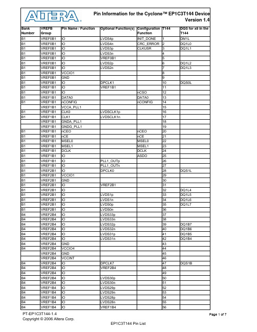
B1VREF0B1IO LVDS4p INIT_DONE1DM1L B1VREF0B1IO LVDS4n CRC_ERROR2DQ1L0 B1VREF0B1IO LVDS3p CLKUSR3DQ1L1 B1VREF0B1IO LVDS3n4B1VREF0B1IO VREF0B15B1VREF0B1IO LVDS2p6DQ1L2 B1VREF0B1IO LVDS2n7DQ1L3 B1VREF0B1VCCIO18B1VREF0B1GND9B1VREF0B1IO DPCLK110DQS0L B1VREF1B1IO VREF1B111B1VREF1B1IO nCSO12B1VREF1B1DATA0DATA013B1VREF1B1nCONFIG nCONFIG14VREF1B1VCCA_PLL115B1VREF1B1CLK0LVDSCLK1p16B1VREF1B1CLK1LVDSCLK1n17VREF1B1GNDA_PLL118VREF1B1GNDG_PLL119B1VREF1B1nCEO nCEO20B1VREF1B1nCE nCE21B1VREF1B1MSEL0MSEL022B1VREF1B1MSEL1MSEL123B1VREF1B1DCLK DCLK24B1VREF1B1IO ASDO25B1VREF1B1IO PLL1_OUTp26B1VREF1B1IO PLL1_OUTn27B1VREF2B1IO DPCLK028DQS1L B1VREF2B1VCCIO129B1VREF2B1GND30B1VREF2B1IO VREF2B131B1VREF2B1IO32DQ1L4 B1VREF2B1IO LVDS1p33DQ1L5 B1VREF2B1IO LVDS1n34DQ1L6 B1VREF2B1IO LVDS0p35DQ1L7 B1VREF2B1IO LVDS0n36B4VREF2B4IO LVDS33p37B4VREF2B4IO LVDS33n38B4VREF2B4IO LVDS32p39DQ1B7 B4VREF2B4IO LVDS32n40DQ1B6 B4VREF2B4IO LVDS31p41DQ1B5 B4VREF2B4IO LVDS31n42DQ1B4 B4VREF2B4GND43B4VREF2B4VCCIO444VREF2B4GND45VREF2B4VCCINT46B4VREF2B4IO DPCLK747DQS1B B4VREF2B4IO VREF2B448B4VREF2B4IO49B4VREF2B4IO LVDS30p50B4VREF2B4IO LVDS30n51B4VREF1B4IO LVDS29p52B4VREF1B4IO LVDS29n53B4VREF1B4IO LVDS28p54B4VREF1B4IO LVDS28n55B4VREF1B4IO VREF1B456B4VREF1B4IO LVDS27p57DM1B B4VREF1B4IO LVDS27n58B4VREF1B4IO LVDS26p59B4VREF0B4IO LVDS26n60B4VREF0B4IO VREF0B461B4VREF0B4IO DPCLK662DQS0B VREF0B4GND63VREF0B4VCCINT64B4VREF0B4GND65B4VREF0B4VCCIO466B4VREF0B4IO LVDS25p67DQ1B3 B4VREF0B4IO LVDS25n68DQ1B2 B4VREF0B4IO LVDS24p69DQ1B1 B4VREF0B4IO LVDS24n70DQ1B0 B4VREF0B4IO LVDS23p71B4VREF0B4IO LVDS23n72B3VREF2B3IO LVDS22n73B3VREF2B3IO LVDS22p74B3VREF2B3IO LVDS21n75B3VREF2B3IO LVDS21p76B3VREF2B3IO LVDS20n77DQ1R7 B3VREF2B3IO LVDS20p78DQ1R6 B3VREF2B3IO VREF2B379B3VREF2B3GND80B3VREF2B3VCCIO381B3VREF2B3IO DPCLK582DQS1R B3VREF2B3IO LVDS19n83DQ1R5 B3VREF2B3IO LVDS19p84DQ1R4 B3VREF2B3IO85DM1R B3VREF1B3CONF_DONE CONF_DONE86B3VREF1B3nSTATUS nSTATUS87B3VREF1B3TCK TCK88B3VREF1B3TMS TMS89B3VREF1B3TDO TDO90B3VREF1B3IO91B3VREF1B3CLK3LVDSCLK2n92B3VREF1B3CLK2LVDSCLK2p93B3VREF1B3IO94B3VREF1B3TDI TDI95B3VREF1B3IO VREF1B396B3VREF0B3IO97DQ1R3 B3VREF0B3IO LVDS18n98DQ1R2 B3VREF0B3IO LVDS18p99DQ1R1 B3VREF0B3IO DPCLK4100DQS0R B3VREF0B3GND101B3VREF0B3VCCIO3102B3VREF0B3IO103DQ1R0 B3VREF0B3IO VREF0B3104B3VREF0B3IO LVDS17n105B3VREF0B3IO LVDS17p106B3VREF0B3IO LVDS16n107B3VREF0B3IO LVDS16p108B2VREF0B2IO LVDS15n109B2VREF0B2IO LVDS15p110B2VREF0B2IO LVDS14n111DQ0T0 B2VREF0B2IO LVDS14p112DQ0T1B2VREF0B2IO LVDS13n113DQ0T2 B2VREF0B2IO LVDS13p114DQ0T3 B2VREF0B2VCCIO2115B2VREF0B2GND116VREF0B2VCCINT117VREF0B2GND118B2VREF0B2IO DPCLK3119DQS0T B2VREF0B2IO VREF0B2120B2VREF0B2IO LVDS12n121B2VREF1B2IO LVDS12p122B2VREF1B2IO LVDS11n123DM0T B2VREF1B2IO LVDS11p124B2VREF1B2IO VREF1B2125B2VREF1B2IO LVDS10n126B2VREF1B2IO LVDS10p127B2VREF1B2IO LVDS9n128B2VREF1B2IO LVDS9p129B2VREF2B2IO LVDS8n130B2VREF2B2IO LVDS8p131B2VREF2B2IO132B2VREF2B2IO VREF2B2133B2VREF2B2IO DPCLK2134DQS1T VREF2B2VCCINT135VREF2B2GND136B2VREF2B2VCCIO2137B2VREF2B2GND138B2VREF2B2IO LVDS7n139DQ0T4 B2VREF2B2IO LVDS7p140DQ0T5 B2VREF2B2IO LVDS6n141DQ0T6 B2VREF2B2IO LVDS6p142DQ0T7 B2VREF2B2IO LVDS5n DEV_OE143B2VREF2B2IO LVDS5p DEV_CLRn144VCCIO[1..4]Power These are I/O supply voltage pins for banks 1 through 4. Each bank can support a different voltage level. VCCIO supplies power to the output buffers for all I/O standards. VCCIO also supplies power to the input buffers used for the LVTTL, LVCMOS, 1.5-V, 1.8-V, 2.5-V, and 3.3-V PCI I/O standards.VCCINT Power These are internal logic array voltage supply pins. VCCINT also supplies power to the input buffers used for the LVDS, SSTL2, and SSTL3 I/O standards.GND Ground Device ground pins. All GND pins should be connected to the board GND plane.VREF[0..2]B[1..4]I/O, Input Input reference voltage for banks 1-4. If a bank uses a voltage-referenced I/O standard, then these pins are used as the voltage-reference pins for the bank. If voltage reference I/O standards are not used in the bank, the VREF pins are available as user I/O pins.VCCA_PLL[1..2]Power Analog power for PLLs[1..2]. The designer must connect this pin to 1.5 V, even if the PLL is not used. GNDA_PLL[1..2]Ground Analog ground for PLLs[1..2]. The designer can connect this pin to the GND plane on the board. GNDG_PLL[1..2]Ground Guard ring ground for PLLs[1..2]. The designer can connect this pin to the GND plane on the board. NC No Connect No connect pins should not be connected on the board. They should be left floating.CONF_DONE Bidirectional (open-drain)This is a dedicated configuration status pin; it is not available as a user I/O pin.nSTATUS Bidirectional (open-drain)This is a dedicated configuration status pin; it is not available as a user I/O pin.nCONFIG Input Dedicated configuration control input. A low transition resets the target device; a low-to-high transition begins configuration. All I/O pins tri-state when nCONFIG is driven low.DCLK Input (PS mode), Output(AS mode)In passive serial configuration mode, DCLK is a clock input used to clock configuration data from an externalsource into the Cyclone device. In active serial configuration mode, DCLK is a clock output from the Cyclonedevice (the Cyclone device acts as master in this mode). This is a dedicated pin used for configuration.DATA0Input Dedicated configuration data input pin.nCE Input Active-low chip enable. Dedicated chip enable input used to detect which device is active in a chain of devices. When nCE is low, the device is enabled. When nCE is high, the device is disabled.nCEO Output Output that drives low when device configuration is complete. During multi-device configuration, this pin feeds a subsequent device’s nCE pin.ASDO I/O, Output Active serial data output from the Cyclone device. This output pin is utilized during active serial configuration mode. The Cyclone device controls configuration and drives address and control information out on ASDO. In passive serial configuration, this pin is available as a user I/O pin.nCSO I/O, Output Chip select output that enables/disables a serial configuration device. This output is utilized during active serial configuration mode. The Cyclone device controls configuration and enables the serial configuration device by driving nCSO low. In passive serial configuration, this pin is available as a user I/O pin.CRC_ERROR I/O, Output Active high signal that indicates that the error detection circuit has detected errors in the configuration SRAM bits. This pin is optional and is used when the CRC error detection circuit is enabled.INIT_DONE I/O, Output (open-drain)This is a dual-purpose pin and can be used as an I/O pin when not enabled as INIT_DONE. When enabled, the pin indicates when the device has entered user mode. This pin can be used as a user I/O pin after configuration.CLKUSR I/O, Input Optional user-supplied clock input. Synchronizes the initialization of one or more devices. This pin can be used as a user I/O pin after configuration.DEV_CLRn I/O, Input Dual-purpose pin that can override all clears on all device registers. When this pin is driven low, all registers are cleared; when this pin is driven high, all registers behave as defined in the design.DEV_OE I/O, Input Dual-purpose pin that can override all tri-states on the device. When this pin is driven low, all I/O pins are tri-stated; when this pin is driven high, all I/O pins behave as defined in the design.MSEL[1..0]Input Dedicated mode select control pins that set the configuration mode for the device. TMS Input This is a dedicated JTAG input pin.TDI Input This is a dedicated JTAG input pin.TCK Input This is a dedicated JTAG input pin.TDO Output This is a dedicated JTAG output pin.CLK0Input, LVDS Input Dedicated global clock input. The dual-function of CLK0 is LVDSCLK1p, which is used for differential input to PLL1.CLK1Input, LVDS Input Dedicated global clock input. The dual-function of CLK1 is LVDSCLK1n, which is used for differential input to PLL1. The EP1C3T100 does not support this clock pin.CLK2Input, LVDS Input Dedicated global clock input. The dual-function of CLK2 is LVDSCLK2p, which is used for differential input to PLL2.Clock and PLL PinsSupply and Reference PinsConfiguration and JTAG PinsCLK3Input, LVDS Input Dedicated global clock input. The dual-function of CLK3 is LVDSCLK2n, which is used for differential input to PLL2. The EP1C3T100 does not support this clock pin.DPCLK[7..0]I/O Dual-purpose clock pins that can connect to the global clock network. These pins can be used for high fan-out control signals, such as clocks, clears, IRDY, TRDY, or DQS signals. These pins are also available as user I/O pins.PLL1_OUTp I/O, Output External clock output from PLL 1. This pin can be used with differential or single ended I/O standards. If clock output from PLL1 is not used, this pin is available as a user I/O pin. The EP1C3T100 does not support this output pin.PLL1_OUTn I/O, Output Negative terminal for external clock output from PLL1. If the clock output is single ended, this pin is available as a user I/O pin. The EP1C3T100 does not support this output pin.LVDS[0..33]p I/O, LVDS RX or TX Dual-purpose LVDS I/O channels 0 to 33. These channels can be used for receiving or transmitting LVDS compatible signals. Pins with a "p" suffix carry the positive signal for the differential channel. If not used for LVDS interfacing, these pins are available as user I/O pins. The EP1C3T100 does not support LVDS I/O interfacing.LVDS[0..33]n I/O, LVDS RX or TX Dual-purpose LVDS I/O channels 0 to 33. These channels can be used for receiving or transmitting LVDS compatible signals. Pins with an "n" suffix carry the negative signal for the differential channel. If not used for LVDS interfacing, these pins are available as user I/O pins. The EP1C3T100 does not support LVDS I/O interfacing.LVDSCLK1p Input, LVDS Input Dual-purpose LVDS clock input to PLL1. If differential input to PLL1 is not required, this pin is available as the CLK0 input pin.LVDSCLK1n Input, LVDS Input Dual-purpose LVDS clock input to PLL1. If differential input to PLL1 is not required, this pin is available as the CLK1 input pin. The EP1C3T100 does not support this clock pinLVDSCLK2p Input, LVDS Input Dual-purpose LVDS clock input to PLL2. If differential input to PLL2 is not required, this pin is available as the CLK2 input pin.LVDSCLK2n Input, LVDS Input Dual-purpose LVDS clock input to PLL2. If differential input to PLL2 is not required, this pin is available as the CLK3 input pin. The EP1C3T100 does not support this clock pin.DQS[0..1][L,R,T,B]I/O Optional data strobe signal for use in external memory interfacing. These pins also function as DPCLK pins; therefore, the DQS signals can connect to the global clock network. A programmable delay chain is used to shift the DQS signals by 90 or 72 degreesDQ[0..7][L,R,T,B]I/O Optional data signal for use in external memory interfacing.DM[0..1][L,R,T,B]I/O Optional data mask output signal for use in external memory interfacing.Dual-Purpose LVDS & External Memory Interface PinsPin Information for the Cyclone™ EP1C3T144 Device, ver 1.4VREF2B2VREF1B2VREF0B2B2V R E F 0B 1B 1B 3V R E F 0B 3V R E F 1B 1V R E F 1B 3PLL1V R E B 2B 1V R E B 2B 3B4VREF2B4VREF1B4VREF0B4Notes:1.This is a top view of the silicon die.2.This is a pictoral representation only to get an idea of placement on the device. Refer to the pin-list andthe Quartus II for exact locations.Version 1.4 Version Number Date Changes Made1.43/6/2006Added CRC_ERROR pin in Pin List and Pin Definitions。

第二种:建立TCL文件进行管脚分配。
这种方法比较灵活,是比较常用的。
这种方法具有分配灵活,方便快捷,可重用性等多方面优点。
方法如下:选择Projects菜单项,并选择Generate tcl file for project选项,系统会为你自动生成相应文件,然后你只要向其中添加你的分配内容就可以了。
还有一种方法就是直接用new ,新建一个TCL文件即可,具体不再细讲。
下面是我分配的内容一部分,可供大家参考。
set_global_assignment -name FAMILY Cycloneset_global_assignment -name DEVICE EP1C3T144C8set_global_assignment -name ORIGINAL_QUARTUS_VERSION 8.0 set_global_assignment -name PROJECT_CREATION_TIME_DATE "19:14:58 JANUARY 06, 2009"set_global_assignment -name LAST_QUARTUS_VERSION 8.0set_global_assignment -nameUSE_GENERATED_PHYSICAL_CONSTRAINTS OFF -section_ideda_palaceset_global_assignment -name DEVICE_FILTER_PACKAGE "ANY QFP" set_global_assignment -name LL_ROOT_REGION ON -section_id "Root Region"set_global_assignment -name LL_MEMBER_STATE LOCKED-section_id "Root Region"set_global_assignment -name DEVICE_FILTER_PIN_COUNT 144 set_global_assignment -name DEVICE_FILTER_SPEED_GRADE 8 set_global_assignment -name FITTER_EFFORT "STANDARD FIT" set_global_assignment -name BDF_FILE topDesign.bdfset_global_assignment -name QIP_FILE nios.qipset_global_assignment -name QIP_FILE altpll0.qipset_global_assignment -name USE_CONFIGURATION_DEVICE ON set_global_assignment -name STRATIX_DEVICE_IO_STANDARD "3.3-V LVTTL"set_global_assignment -name PARTITION_NETLIST_TYPE SOURCE -section_id Topset_global_assignment -name PARTITION_COLOR 14622752-section_id Topset_location_assignment PIN_72 -to addr[7]set_location_assignment PIN_69 -to addr[6]set_location_assignment PIN_70 -to addr[5]set_location_assignment PIN_67 -to addr[4]set_location_assignment PIN_68 -to addr[3]set_location_assignment PIN_42 -to addr[2]set_location_assignment PIN_39 -to addr[1]set_location_assignment PIN_40 -to addr[0]set_location_assignment PIN_48 -to data[15]set_location_assignment PIN_47 -to data[14]set_location_assignment PIN_50 -to data[13]set_location_assignment PIN_49 -to data[12]set_location_assignment PIN_56 -to data[11]set_location_assignment PIN_55 -to data[10]set_location_assignment PIN_58 -to data[9]set_location_assignment PIN_57 -to data[8]set_location_assignment PIN_61 -to data[7]set_location_assignment PIN_62 -to data[6]set_location_assignment PIN_59 -to data[5]set_location_assignment PIN_60 -to data[4]set_location_assignment PIN_53 -to data[3]set_location_assignment PIN_54 -to data[2]set_location_assignment PIN_51 -to data[1]set_location_assignment PIN_52 -to data[0]set_location_assignment PIN_16 -to clkset_location_assignment PIN_38 -to csset_location_assignment PIN_141 -to led[3]set_location_assignment PIN_142 -to led[2]set_location_assignment PIN_143 -to led[1]set_location_assignment PIN_144 -to led[0]set_location_assignment PIN_33 -to reset_nset_location_assignment PIN_41 -to rdset_location_assignment PIN_71 -to wrset_location_assignment PIN_105 -to mosiset_location_assignment PIN_107 -to sclkset_location_assignment PIN_106 -to ssset_location_assignment PIN_73 -to motor[0]set_location_assignment PIN_74 -to motor[1]set_location_assignment PIN_75 -to motor[2]set_location_assignment PIN_76 -to motor[3]set_instance_assignment -name PARTITION_HIERARCHY root_partition -to | -section_id Top# Commit assignmentsexport_assignmentsFPGA 点滴(2008-09-30 09:44:45)转载标签:杂谈以此记录心得以及重要的知识点。

EP1C3T144FPGAdevelopboardmanual(开发板原理图)FPGA develop board manual ALTERA Cyclone EP1C3T144ALTERA Cyclone 系列的fpga是altera 公司针对底端用户推出的一个系列的fpga。
具有成本低,使用的方便的优点,规模从3000到20000LE。
这一块实验板用的EP1C3T144的芯片,有3000LE逻辑资源,另外还有13条M4K RAM (共6.5Kbyte),另外还有还有一个数字锁相环。
这些资源能够足够应付电子设计竞赛和日常教学的需要,也可以作为初学者入门学习fpga的工具。
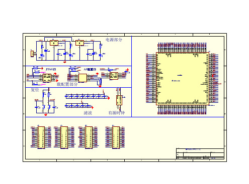
1. 开发板介绍1.1. 总体介绍开发板的电路图,如附录所示,电路图一共可分为9个部分:电源部分、按键和LED、下载配置部分、复位部分、外部时钟、滤波电容、用户扩展接口、5 1单片机接口、FPGA 芯片。
1.2. 具体介绍1.2.1. 电源部分板子由外部提供5V电源,使用的圆头插座的封装,可以直接用5V的电源适配器插上使用,不需要直流稳压电源,FPGA的IO的电源是3.3V,内核的电压是1.5V,所以用上两个LEO,一个将5V转到3.3V,另一个将3.3V转到1.5V,加上一些滤波电容,板上的其他外设的电源均是3.3V,另外有3.3V的电源指示灯,表示电源是否正常,还有防反插二极管,防止电源反插,对器件造成损坏。
1.2.2. 按键和LED板上提供4个拨码按键和4个led,分别接到fpga的8个IO引脚上,具体的引脚可以参看电路图或者丝印。
对于初学者,按键和led 可以用外当成最简单的外设,用和来控制这些外设。
对于用该板作开发的用户来说,可以把按键当成键盘控制,而把led当成提示来用。
1.2.3. 下载配置部分大家都知道fpga是sram型的可编程逻辑器件,不像rom型可编程器件cpld那样,通过jtag就可以直接把代码固化片子里面。
B1VREF0B1IO INIT_DONE1B1VREF0B1IO CRC_ERROR2B1VREF0B1IO CLKUSR3B1VREF0B1IO VREF0B14B1VREF0B1VCCIO1B1VREF0B1GNDB1VREF1B1IO VREF1B15B1VREF1B1IO nCSO6B1VREF1B1DATA0DATA07B1VREF1B1nCONFIG nCONFIG8VREF1B1VCCA_PLL19B1VREF1B1CLK010VREF1B1GNDA_PLL111B1VREF1B1nCEO nCEO12B1VREF1B1nCE nCE13B1VREF1B1MSEL0MSEL014B1VREF1B1MSEL1MSEL115B1VREF1B1DCLK DCLK16B1VREF1B1IO ASDO17B1VREF2B1VCCIO118B1VREF2B1GND19B1VREF2B1IO VREF2B120B1VREF2B1IO21B1VREF2B1IO22B1VREF2B1IO23B1VREF2B1IO24B1VREF2B1IO25B4VREF2B4IO26B4VREF2B4IO27DQ1B7 B4VREF2B4IO28DQ1B6 B4VREF2B4IO29DQ1B5 B4VREF2B4GND30B4VREF2B4VCCIO431VREF2B4GND32VREF2B4VCCINT33B4VREF2B4IO DPCLK734DQS1B B4VREF2B4IO VREF2B435B4VREF2B4IO36DQ1B4 B4VREF1B4IO37B4VREF1B4IO VREF1B438B4VREF1B4IO39DM1B B4VREF1B4IO40B4VREF0B4IO VREF0B441B4VREF0B4IO DPCLK642DQS0B VREF0B4GND43VREF0B4VCCINT44B4VREF0B4GND45B4VREF0B4VCCIO446B4VREF0B4IO47DQ1B3 B4VREF0B4IO48DQ1B2 B4VREF0B4IO49DQ1B1 B4VREF0B4IO50DQ1B0 B3VREF2B3IO51B3VREF2B3IO52B3VREF2B3IO53DQ0R7 B3VREF2B3IO54DQ0R6B3VREF2B3IO55DQ0R5 B3VREF2B3IO56DQ0R4 B3VREF2B3IO VREF2B357B3VREF2B3GND58B3VREF2B3VCCIO359B3VREF1B3CONF_DONE CONF_DONE60B3VREF1B3nSTATUS nSTATUS61B3VREF1B3TCK TCK62B3VREF1B3TMS TMS63B3VREF1B3TDO TDO64B3VREF1B3IO65DM0R B3VREF1B3CLK266B3VREF1B3TDI TDI67B3VREF1B3IO VREF1B368B3VREF0B3IO69DQ0R3 B3VREF0B3IO70DQ0R2 B3VREF0B3IO71DQ0R1 B3VREF0B3IO DPCLK472DQS0R B3VREF0B3GNDB3VREF0B3VCCIO3B3VREF0B3IO VREF0B373B3VREF0B3IO74DQ0R0 B3VREF0B3IO75B2VREF0B2IO76DQ1T0 B2VREF0B2IO77DQ1T1 B2VREF0B2IO78DQ1T2 B2VREF0B2IO79DQ1T3 B2VREF0B2VCCIO280B2VREF0B2GND81VREF0B2VCCINT82VREF0B2GND83B2VREF0B2IO DPCLK384DQS0T B2VREF0B2IO VREF0B285B2VREF1B2IO86B2VREF1B2IO87B2VREF1B2IO VREF1B288B2VREF1B2IO89B2VREF2B2IO90DM1T B2VREF2B2IO VREF2B291B2VREF2B2IO DPCLK292DQS1T VREF2B2VCCINT93VREF2B2GND94B2VREF2B2VCCIO295B2VREF2B2GND96B2VREF2B2IO97DQ1T4 B2VREF2B2IO98DQ1T5 B2VREF2B2IO DEV_OE99DQ1T6 B2VREF2B2IO DEV_CLRn100DQ1T7VCCIO[1..4]Power These are I/O supply voltage pins for banks 1 through 4. Each bank can support a different voltage level. VCCIO supplies power to the output buffers for all I/O standards. VCCIO also supplies power to the input buffers used for the LVTTL, LVCMOS, 1.5-V, 1.8-V, 2.5-V, and 3.3-V PCI I/O standards.VCCINT Power These are internal logic array voltage supply pins. VCCINT also supplies power to the input buffers used for the LVDS, SSTL2, and SSTL3 I/O standards.GNDGroundDevice ground pins. All GND pins should be connected to the board GND plane.VREF[0..2]B[1..4]I/O, Input Input reference voltage for banks 1-4. If a bank uses a voltage-referenced I/O standard, then these pins are used as the voltage-reference pins for the bank. If voltage reference I/O standards are not used in the bank, the VREF pins are available as user I/O pins.VCCA_PLL1Power Analog power for PLL1. The designer must connect this pin to 1.5 V, even if the PLL is not used.GNDA_PLL1Ground Analog ground for PLL1. The designer can connect this pin to the GND plane on the board.NCNo Connect No connect pins should not be connected on the board. They should be left floating.CONF_DONE Bidirectional (open-drain)This is a dedicated configuration status pin; it is not available as a user I/O pin.nSTATUS Bidirectional (open-drain)This is a dedicated configuration status pin; it is not available as a user I/O pin.nCONFIGInputDedicated configuration control input. A low transition resets the target device; a low-to-high transition begins configuration. All I/O pins tri-state when nCONFIG is driven low.DCLK Input (PS mode), Output (AS mode)In passive serial configuration mode, DCLK is a clock input used to clock configuration data from an external source into the Cyclone device. In active serial configuration mode, DCLK is a clock outputfrom the Cyclone device (the Cyclone device acts as master in this mode). This is a dedicated pin used for configuration.DATA0InputDedicated configuration data input pin.nCE Input Active-low chip enable. Dedicated chip enable input used to detect which device is active in a chain of devices. When nCE is low, the device is enabled. When nCE is high, the device is disabled.nCEOOutputOutput that drives low when device configuration is complete. During multi-device configuration, this pin feeds a subsequent device’s nCE pin.ASDO I/O, OutputActive serial data output from the Cyclone device. This output pin is utilized during active serial configuration mode. The Cyclone device controls configuration and drives address and control information out on ASDO. In passive serial configuration, this pin is available as a user I/O pin.nCSO I/O, OutputChip select output that enables/disables a serial configuration device. This output is utilized during active serial configuration mode. The Cyclone device controls configuration and enables the serial configuration device by driving nCSO low. In passive serial configuration, this pin is available as a user I/O pin.CRC_ERRORI/O, OutputActive high signal that indicates that the error detection circuit has detected errors in the configuration SRAM bits. This pin is optional and is used when the CRC error detection circuit is enabled.INIT_DONE I/O, Output (open-drain)This is a dual-purpose pin and can be used as an I/O pin when not enabled as INIT_DONE. When enabled, the pin indicates when the device has entered user mode. This pin can be used as a user I/Opin after configuration.CLKUSRI/O, InputOptional user-supplied clock input. Synchronizes the initialization of one or more devices. This pin can be used as a user I/O pin after configuration.DEV_CLRn I/O, InputDual-purpose pin that can override all clears on all device registers. When this pin is driven low, all registers are cleared; when this pin is driven high, all registers behave as defined in the design.DEV_OE I/O, Input Dual-purpose pin that can override all tri-states on the device. When this pin is driven low, all I/O pins are tri-stated; when this pin is driven high, all I/O pins behave as defined in the design.MSEL[1..0]Input Dedicated mode select control pins that set the configuration mode for the device.TMS Input This is a dedicated JTAG input pin.TDI Input This is a dedicated JTAG input pin.TCK Input This is a dedicated JTAG input pin.TDO Output This is a dedicated JTAG output pin.CLK0Input Dedicated global clock input.CLK2InputDedicated global clock input.Clock and PLL PinsSupply and Reference PinsConfiguration and JTAG PinsDPCLK[7, 6, 4, 3, 2]I/O Dual-purpose clock pins that can connect to the global clock network. These pins can be used for high fan-out control signals, such as clocks, clears, IRDY, TRDY, or DQS signals. These pins are also available as user I/O pins.DQS[0..1][L,R,T,B]I/O Optional data strobe signal for use in external memory interfacing. These pins also function as DPCLK pins; therefore, the DQS signals can connect to the global clock network. A programmable delay chain is used to shift the DQS signals by 90 or 72 degrees.DQ[0..7][L,R,T,B]I/O Optional data signal for use in external memory interfacing.DM[0..1][L,R,T,B]I/O Optional data mask output signal for use in external memory interfacing.Dual-Purpose External Memory Interface PinsPin Information for the Cyclone™ EP1C3T100 Device, ver 1.5VREF2B2VREF1B2VREF0B2B2V R E F 0B 1B 1B 3V R E F 0B 3V R E F 1B 1V R E F 1B 3PLL1V R E B 2B 1V R E B 2B 3B4VREF2B4VREF1B4VREF0B4Notes:1.This is a top view of the silicon die.2.This is a pictoral representation only to get an idea of placement on the device. Refer to the pin-list andthe Quartus II for exact locations.Version 1.5 Version Number Date Changes Made1.53/6/2006Added CRC_ERROR pin in Pin List and Pin Definitions。
实验一Quartus II开发环境入门一、实验目的1、了解QuartusII软件及基本操作2、熟悉图形编辑器Block Builder/Schematic File的设计输入3、掌握电路的编译和适配4、掌握电路仿真与时序分析5、熟悉3/8线译码器工作原理和五人表决器设计二、实验原理1、以3/8线译码器为例,总体思路以EP1C3中的三个拨位开关,SW3,SW2,SW1为三个输入信号,可以代表8种不同的状态,该译码器对这8种状态译码,并把所译码的结果在七个彩灯上显示。
2、三、实验步骤主要仪器和设备:计算机,EDA实验箱。
步骤一:1、建立工程,设计输入。
选择菜单“File”→“New Preject Wizard”将设计文件加入工程中:点击下方的“Next” 按钮,在弹出的对话框中点击“File”栏的按钮,将此工程相关的所有VHDL文件加入进此工程(如果有的话)。
Cyclone系列的EP1C3T144C8按下“Next”后,出现仿真工具选择对话框。
不作任何选择。
4、完成设置点击“Next”后,完成工程的设定,点击“finish”。
步骤二:1、选择File/New或点击主菜单中的空白图标,进入新建程序文件状态,选择VHDL file 。
VHDL程序文件的扩展名是:* .vhd程序代码:-- A simple 3 to 8 decoderlibrary ieee;use ieee.std_logic_1164.all;entity decoder isport ( inp: in std_logic_vector(2 downto 0);outp: out std_logic_vector(7 downto 0)); end decoder;architecture behave of decoder isbeginoutp(0) <= '1' when inp = "000" else '0';outp(1) <= '1' when inp = "001" else '0';outp(2) <= '1' when inp = "010" else '0';outp(3) <= '1' when inp = "011" else '0';outp(4) <= '1' when inp = "100" else '0';outp(5) <= '1' when inp = "101" else '0';outp(6) <= '1' when inp = "110" else '0';outp(7) <= '1' when inp = "111" else '0';end behave;步骤三:1、选择菜单“File”→“New ” →“ Schematic File”,即弹出原理图编辑框。