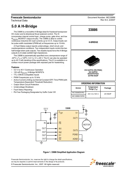
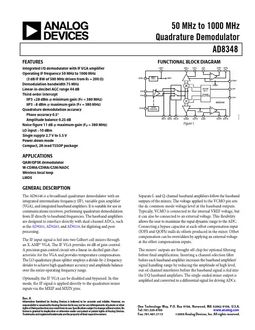
50 MHz to 1000 MHzQuadrature DemodulatorAD8348 Rev. AInformation furnished by Analog Devices is believed to be accurate and reliable. However, noresponsibility is assumed by Analog Devices for its use, nor for any infringements of patents or other rights of third parties that may result from its use. Specifications subject to change without notice. No license is granted by implication or otherwise under any patent or patent rights of Analog Devices. T rademarks and registered trademarks are the property of their respective owners. One Technology Way, P.O. Box 9106, Norwood, MA 02062-9106, U.S.A. Tel: 781.329.4700 Fax: 781.461.3113 ©2006 Analog Devices, Inc. All rights reserved.FEATURESIntegrated I/Q demodulator with IF VGA amplifier Operating IF frequency 50 MHz to 1000 MHz(3 dB IF BW of 500 MHz driven from R S = 200 Ω) Demodulation bandwidth 75 MHzLinear-in-decibel AGC range 44 dBThird-order interceptIIP3 +28 dBm @ minimum gain (F IF = 380 MHz) IIP3 −8 dBm @ maximum gain (F IF = 380 MHz) Quadrature demodulation accuracyPhase accuracy 0.5°Amplitude balance 0.25 dBNoise figure 11 dB @ maximum gain (F IF = 380 MHz) LO input −10 dBmSingle supply 2.7 V to 5.5 VPower-down modeCompact, 28-lead TSSOP packageAPPLICATIONSQAM/QPSK demodulatorW-CDMA/CDMA/GSM/NADCWireless local loopLMDS FUNCTIONAL BLOCK DIAGRAM3678-1Figure 1.GENERAL DESCRIPTIONThe AD8348 is a broadband quadrature demodulator with an integrated intermediate frequency (IF), variable gain amplifier (VGA), and integrated baseband amplifiers. It is suitable for use in communications receivers, performing quadrature demodulation from IF directly to baseband frequencies. The baseband amplifiers are designed to interface directly with dual-channel ADCs, such as the AD9201, AD9283, and AD9218, for digitizing and post-processing.The IF input signal is fed into two Gilbert cell mixers through an X-AMP® VGA. The IF VGA provides 44 dB of gain control.A precision gain control circuit sets a linear-in-decibel gain char-acteristic for the VGA and provides temperature compensation. The LO quadrature phase splitter employs a divide-by-2 frequency divider to achieve high quadrature accuracy and amplitude balance over the entire operating frequency range.Optionally, the IF VGA can be disabled and bypassed. In this mode, the IF signal is applied directly to the quadrature mixer inputs via the MXIP and MXIN pins. Separate I- and Q-channel baseband amplifiers follow the baseband outputs of the mixers. The voltage applied to the VCMO pin sets the dc common-mode voltage level at the baseband outputs. Typically, VCMO is connected to the internal VREF voltage, but it can also be connected to an external voltage. This flexibility allows the user to maximize the input dynamic range to the ADC. Connecting a bypass capacitor at each offset compensation input (IOFS and QOFS) nulls dc offsets produced in the mixer. Offset compensation can be overridden by applying an external voltage at the offset compensation inputs.The mixers’ outputs are brought off-chip for optional filtering before final amplification. Inserting a channel selection filter before each baseband amplifier increases the baseband amplifiers’ signal handling range by reducing the amplitude of high level, out-of-channel interferers before the baseband signal is fed into the I/Q baseband amplifiers. The single-ended mixer output is amplified and converted to a differential signal for driving ADCs.AD8348Rev. A | Page 2 of 28TABLE OF CONTENTSFeatures..............................................................................................1 Applications.......................................................................................1 Functional Block Diagram..............................................................1 General Description.........................................................................1 Revision History...............................................................................2 Specifications.....................................................................................3 Absolute Maximum Ratings............................................................6 ESD Caution..................................................................................6 Pin Configuration and Function Descriptions.............................7 Equivalent Circuits...........................................................................9 Typical Performance Characteristics...........................................11 VGA and Demodulator.............................................................11 Demodulator Using MXIP and MXIN....................................14 Final Baseband Amplifiers........................................................15 VGA/Demodulator and Baseband Amplifier.........................16 Theory of Operation......................................................................18 VGA..............................................................................................18 Downconversion Mixers...........................................................18 Phase Splitter...............................................................................18 I/Q Baseband Amplifiers...........................................................18 Enable...........................................................................................18 Baseband Offset Cancellation...................................................18 Applications.....................................................................................20 Basic Connections......................................................................20 Power Supply...............................................................................20 Device Enable.............................................................................20 VGA Enable................................................................................20 Gain Control...............................................................................20 LO Inputs.....................................................................................20 IF Inputs......................................................................................20 MX Inputs...................................................................................20 Baseband Outputs......................................................................21 Output DC Bias Level................................................................21 Interfacing to Detector for AGC Operation...............................21 Baseband Filters..........................................................................22 LO Generation............................................................................23 Evaluation Board........................................................................23 Outline Dimensions.......................................................................28 Ordering Guide.. (28)REVISION HISTORY4/06—Rev. 0 to Rev. AUpdated Format..................................................................Universal Changes to Specifications................................................................3 Changes to IF Inputs Section........................................................20 Changes to Evaluation Board Section..........................................23 Changes to Table 6..........................................................................27 Changes to Ordering Guide..........................................................28 8/03—Revision 0: Initial VersionAD8348Rev. A | Page 3 of 28SPECIFICATIONSV S = 5 V , T A = 25o C, F LO = 380 MHz, F IF = 381 MHz, P LO = −10 dBm, R S (LO) = 50 Ω, R S (IFIP and MXIP/MXIN) = 200 Ω, unless otherwise noted. Table 1.Parameter Conditions Min Typ Max Unit OPERATING CONDITIONS LO Frequency Range External input = 2 × LO frequency 100 2000 MHz IF Frequency Range 50 1000 MHz Baseband Bandwidth 75 MHz LO Input Level 50 Ω source −12 −10 0 dBm V SUPPLY (V S ) 2.7 5.5 V Temperature Range −40 +85 °C IF FRONT END WITH VGA IFIP to IMXO (QMXO), ENVG = 5 V, IMXO/QMXO load = 1.5 kΩ Input Impedance Measured differentially across MXIP/MXIN 200||1.1 Ω||pF Gain Control Range 44 dB Maximum Conversion Voltage Gain VGIN = 0.2 V (maximum voltage gain) 25.5 dB Minimum Conversion Voltage Gain VGIN = 1.2 V (minimum voltage gain) −18.5 dB 3 dB Bandwidth 500 MHz Gain Control Linearity VGIN = 0.4 V (+21 dB) to 1.1 V (−14 dB) ±0.5 dB IF Gain Flatness F IF = 380 MHz ± 5% (VGIN = 1.2 V) 0.1 dB p-p F IF = 900 MHz ± 5% (VGIN = 1.2 V) 1.3 dB p-p Input 1 dB Compression Point (P1dB) VGIN = 0.2 V (maximum gain) −22 dBmVGIN = 1.2 V (maximum gain) +13 dBm Second-Order Input Intercept (IIP2) IF1 = 385 MHz, IF2 = 386 MHz+3 dBm each tone from 200 Ω source, 65 dBm VGIN = 1.2 V (minimum gain)−42 dBm each tone from 200 Ω source, 18 dBmVGIN = 0.2 V (maximum gain) Third-Order Input Intercept (IIP3) IF1 = 381 MHz, IF2 = 381.02 MHz Each tone 10 dB below P1dB from 200 Ω source,28 dBm VGIN = 1.2 V (minimum gain)Each tone 10 dB below P1dB from 200 Ω source,−8 dBmVGIN = 0.2 V (maximum gain)LO Leakage Measured at IFIP , IFIN −80 dBm Measured at IMXO/QMXO (LO = 50 MHz) −60 dBm Demodulation Bandwidth Small signal 3 dB bandwidth 75 MHz Quadrature Phase Error 1LO = 380 MHz (LOIP/LOIN 760 MHz) −0.7 ±0.1 +0.7 Degrees vs. temperature −0.0032 °/°C vs. baseband frequency (dc to 30 MHz) +0.01 °/MHzI/Q Amplitude Imbalance 1−0.3 ±0.05 +0.3 dB vs. temperature 0 dB/°C vs. baseband frequency (dc to 30 MHz) ±0.0125 dB Noise Figure (Double Sideband) Maximum gain, from 200 Ω source,F IF = 380 MHz10.75 dB Mixer Output Impedance 40 Ω Capacitive Load Shunt from IMXO, QMXO to VCMO 0 10 pF Resistive LoadShunt from IMXO, QMXO to VCMO 200 1.5 kΩ Mixer Peak Output Current 2.5 mAAD8348Rev. A | Page 4 of 28Parameter Conditions Min Typ Max Unit IF FRONT END WITHOUT VGA From MXIP , MXIN to IMXO (QMXO), ENVG = 0 V, IMXO/QMXO load = 1.5 kΩ Input Impedance Measured differentially across MXIP/MXIN 200||1.5 Ω||pF Conversion voltage Gain 10.5 dB 3 dB Output Bandwidth 75 MHz IF Gain Flatness F IF = 380 MHZ ± 5% 0.1 dB p-p F IF = 900 MHZ ± 5% 0.15 dB p-p Input 1 dB Compression Point (P1dB) −4 dBm Third-Order Input Intercept (IIP3) IF1 = 381 MHz, IF2 = 381.02 MHz 14 dBm Each tone 10 dB below P1dB from200 Ω sourceLO Leakage Measured at MXIP/MXIN −70 dBm Measured at IMXO, QMXO −60 dBm Demodulation Bandwidth Small signal 3 dB bandwidth 75 MHz Quadrature Phase Error LO = 380 MHz (LOIP/LOIN 760 MHz,single-ended)−2 ±0.5 +2 Degrees I/Q Amplitude Imbalance 0.25 dB Noise Figure (Double Sideband) From 200 Ω source, F IF = 380 MHz 21 dB I/Q BASEBAND AMPLIFIER From IAIN to IOPP/IOPN and QAIN to QOPP/QOPN, R LOAD = 2 kΩ, single-ended to groundGain 20 dB Bandwidth 10 pF differential load 125 MHz Output DC Offset (Differential) LO leakage offset corrected using 500 pFcapacitor on IOFS, QOFS (V IOPP − V IOPN )−50 ±12 +50 mV Output Common-Mode Offset (V IOPP + V IOPN )/2 − VCMO −75 ±35 +75 mV Group Delay Flatness 0 MHz to 50 MHz 3 ns p-p Input-Referred Noise Voltage Frequency = 1 MHz 8 nV/√Hz Output Swing Limit (Upper) V S −1 V Output Swing Limit (Lower) 0.5 V Peak Output Current 1 mA Input Impedance 50||1 kΩ||pF Input Bias Current 2 μARESPONSE FROM IF AND MX INPUTS TO BASEBAND AMPLIFIER OUTPUT IMXO and QMXO connected directly toIAIN and QAIN, respectivelyGain From MX I P/MX I N 30.5 dB From IFIP/IFIN, VGIN = 0.2 V 45.5 dB From IFIP/IFIN, VGIN = 1.2 V 1.5 dB CONTROL INPUT/OUTPUTS VCMO Input Range V S = 5 V 0.5 1 4 V V S = 2.7 V 0.5 1 1.7 V VREF Output Voltage 0.95 1 1.05 V Gain Control Voltage Range VGIN 0.2 1.2 V Gain Slope −55 −50 −45 dB/V Gain Intercept Linear extrapolation back to theoreticalgain at VGIN = 0 V55 61 67 dB Gain Control Input Bias Current 1 μA LO INPUTSLOIP Input Return Loss LOIN ac-coupled to ground(760 MHz applied to LOIP)−6 dBAD8348Rev. A | Page 5 of 28Parameter Conditions Min Typ Max Unit POWER-UP CONTROL ENBL Threshold Low Low = standby 0 V S /2 1 V ENBL Threshold High High = enable V S − 1 V S /2 V S V Input Bias Current 2 μA Power-Up Time Time for final baseband amplifiers to bewithin 90% of final amplitude45 μs Power-Down Time Time for supply current to be <10% ofenabled value700 ns POWER SUPPLIES VPOS1, VPOS2, VPOS3Voltage 2.7 5.5 V Current (Enabled) V S = 5 V, V ENBL = 5 V 38 48 58 mA Current (Standby) V S = 5 V, V ENBL = 0 V 75 μA1These parameters are guaranteed but not tested in production. Limits are ±6 Σ from the mean.AD8348Rev. A | Page 6 of 28ABSOLUTE MAXIMUM RATINGSTable 2.Parameter RatingSupply Voltage on VPOS1, VPOS2, VPOS3 Pins 5.5 VLO Input Power 10 dBm (re: 50 Ω)IF Input Power 18 dBm (re: 200 Ω)Internal Power Dissipation 450 mWθJA 68°C/WMaximum Junction Temperature 150°C Operating Temperature Range −40°C to +85°C Storage Temperature Range −65°C to +125°CLead Temperature (Soldering, 60 sec) 300°CStresses above those listed under Absolute Maximum Ratings may cause permanent damage to the device. This is a stressrating only; functional operation of the device at these or anyother conditions above those indicated in the operationalsection of this specification is not implied. Exposure to absolutemaximum rating conditions for extended periods may affectdevice reliability.ESD CAUTIONESD (electrostatic discharge) sensitive device. Electrostatic charges as high as 4000 V readily accumulate on the human body and test equipment and can discharge without detection. Although this product features proprietary ESD protection circuitry, permanent damage may occur on devices subjected to high energy electrostatic discharges. Therefore, proper ESD precautions are recommended to avoid performancedegradation or loss of functionality.AD8348Rev. A | Page 7 of 28PIN CONFIGURATION AND FUNCTION DESCRIPTIONSLOIPVPOS1IOPN IOPP VCMO IAIN COM3IMXO COM2IFIN IFIP VPOS2IOFS VREF 03678-002Figure 2. 28-Lead TSSOP Pin ConfigurationTable 3. Pin Function Descriptions—28-Lead TSSOPPin No. Mnemonic DescriptionEquivalent Circuit 1, 28LOIP , LOINLO Inputs. For optimum performance, these inputs should be ac-coupled and driven differentially. Differential drive from single-ended sources can be achieved via a balun. To obtain a broadband 50 Ω input impedance, connect a 60.4 Ω shunt resistor between LOIP and LOIN. Typical input drive level is equal to −10 dBm.A2, 12, 20 VPOS1, VPOS2, VPOS3 Positive Supply for LO, IF, and Biasing and Baseband Sections, Respectively. These pinsshould be decoupled with 0.1 μF and 100 pF capacitors.3, 4, 25, 26 IOPN, IOPP , QOPP , QOPN I- and Q-Channel Differential Baseband Outputs. Typical output swing is equal to 2 V p-pdifferential. The dc common-mode voltage level on these pins is set by the voltage on VCMO.B 5 VCMO Baseband DC Common-Mode Voltage. The voltage applied to this pin sets the dccommon-mode levels for all the baseband outputs and inputs (IMXO, QMXO, IOPP , IOPN, QOPP , QOPN, IAIN, and QAIN). This pin can be connected either to VREF or to a reference voltage from another device (typically an ADC).C6, 23 IAIN, QAIN I- and Q-Channel Baseband Amplifier Inputs. The single-ended signals on these pins arereferenced to VCMO and must have a dc bias equal to the dc voltage on the VCMO pin. If IMXO (QMXO) is dc-coupled to IAIN (QAIN), biasing will be provided by IMXO (QMXO). If an ac-coupled filter is placed between IMXO and IAIN, these pins can be biased from the source driving VCMO through a 1 kΩ resistor. The gain from IAIN/QAIN to the differential outputs (IOPP/IOPN and QOPP/QOPN) is 20 dB.D7, 22 COM3 Ground for Biasing and Baseband Sections. 8, 21 IMXO, QMXO I- and Q-Channel Mixer Baseband Outputs. These are low impedance (40 Ω) outputs whosebias levels are set by the voltage applied to the VCMO pin. These pins are typically connected to IAIN and QAIN, respectively, either directly or through a filter. Each output can drive a maximum current of 2.5 mA.H9 COM2 IF Section Ground. 10, 11 IFIN, IFIP IF Inputs. IFIN should be ac-coupled to ground. The single-ended IF input signal shouldbe ac-coupled into IFIP . The nominal differential input impedance of these pins is 200 Ω. For a broadband 50 Ω input impedance, a minimum-loss L pad should be used; R SERIES = 174 Ω, R SHUNT = 57.6 Ω. This provides a 200 Ω source impedance to the IF input. However, the AD8348 does not necessarily require a 200 Ω source impedance, and a single shunt 66.7 Ω resistor can be placed between IFIP and IFIN.E13, 16 IOFS, QOFS I- and Q-Channel Offset Nulling Inputs. DC offsets on the I-channel mixer output (IMXO)can be nulled by connecting a 0.1 μF capacitor from IOFS to ground. Driving IOFS with a fixed voltage (typically a DAC calibrated such that the offset at IOPP/IOPN is nulled) can extend the operating frequency range to include dc. The QOFS pin can likewise be used to null offsets on the Q-channel mixer output (QMXO).F14 VREF Reference Voltage Output. This output voltage (1 V) is the main bias level for the deviceand can be used to externally bias the inputs and outputs of the baseband amplifiers. The typical maximum drive current for this output is 2 mA.GAD8348Rev. A | Page 8 of 28Pin No. Mnemonic Description EquivalentCircuit 15 ENBL Chip Enable Input. Active high. Threshold is equal to V S /2. D 17 VG IN Gain Control Input. The voltage on this pin controls the gain on the IF VGA. The gain control voltage range is from 0.2 V to 1.2 V and corresponds to a conversion gain range from +25.5 dB to −18.5 dB. This is the gain to the output of the mixers (that is, IMXO and QMXO). There is an additional 20 dB of fixed gain in the final baseband amplifiers (IAIN to IOPP/IOPN and QAIN to QOPP/QOPN). Note that the gain control function has a negative sense (that is, increasing voltage decreases gain).D18, 19 MXIP , MXIN Auxiliary Mixer Inputs. If ENVG is low, the IFIP and IFIN inputs are disabled and MXIP and MXIN are enabled, allowing the VGA to be bypassed. The auxiliary mixer inputs are fully differential inputs that should be ac-coupled to the signal source.I24 ENVG Active High VGA Enable. When ENVG is high, IFIP and IFIN inputs are enabled and MXIP and MXIN inputs are disabled. When ENVG is low, MXIP and MXIN inputs are enabled and IFIP and IFIN inputs are disabled.D27 COM1 LO Section Ground.AD8348Rev. A | Page 9 of 28EQUIVALENT CIRCUITSLOIN LOIP03678-003Figure 3. Circuit A VCMOVPOS3IOPP , IOPN,QOPP , QOPN 03678-004Figure 4. Circuit BVCMO03678-005Figure 5. Circuit C 03678-006Figure 6. Circuit DVPOS2IFIPIFIN03678-007Figure 7. Circuit E03678-008Figure 8. Circuit FAD8348Rev. A | Page 10 of 2803678-009Figure 9. Circuit G03678-010Figure 10. Circuit H03678-011Figure 11. Circuit IRev. A | Page 11 of 28TYPICAL PERFORMANCE CHARACTERISTICSVGA AND DEMODULATORVGIN (V)V G A A N D M I X E R G A I N (d B )L I N E A R I T Y E R R O R (d B )0.20.30.4–20–5–10–15105030252015–6–3–4–50–1–243210.50.60.70.80.9 1.0 1.1 1.203678-012Figure 12. Mixer Gain and Linearity Error vs. VGIN, V POS = 5 V, F IF = 380 MHz,F BB = 1 MHz, Temperature = −40°C, +25°C, +85°CVGIN (V)V G A A N D M I X E R G A I N (d B )L I N E A R I T Y E R R O R (d B )0.20.30.4–25–10–15–2050–525201510–6–3–4–50–1–243210.50.60.70.80.9 1.0 1.1 1.203678-013Figure 13. Mixer Gain and Linearity Error vs. VGIN, V POS = 5 V, F IF = 900 MHz,F BB = 1 MHz, Temperature = −40°C, +25°C, +85°C VGIN (V)V G A A N D M I X E R G A I N (d B )L I N E A R I T Y E R R O R (d B )0.20.30.4–6–3–4–50–1–243210.50.60.70.80.91.01.11.203678-014Figure 14. Mixer Gain and Linearity Error vs. VGIN, V POS = 2.7 V, F IF = 380 MHz,F BB = 1 MHz, Temperature = −40°C, +25°C, +85°CVGIN (V)V G A A N D M I X E R G A I N (d B )L I N E A R I T Y E R R O R (d B )0.20.30.4–25–10–15–2050–525201510–6–3–4–50–1–243210.50.60.70.80.91.01.11.203678-015Figure 15. Mixer Gain and Linearity Error vs. VGIN, V POS = 2.7 V, F IF = 900 MHz,F BB = 1 MHz, Temperature = −40°C, +25°C, +85°CIF FREQUENCY (MHz)V G A A N D M I X E R G A I N (d B )100182022242628200300400500600700800900100003678-016Figure 16. Gain vs. F IF , VGIN = 0.2 V, F BB = 1 MHz,Temperature = −40°C, +25°C, +85°CIF FREQUENCY (MHz)V G A A N D M I X E R G A I N (d B )100–30–25–20–15200300400500600700800900100003678-017Figure 17. Gain vs. F IF , VGIN = 1.2 V, F BB = 1 MHz,Temperature = −40°C, +25°C, +85°CRev. A | Page 12 of 28BASEBAND FREQUENCY (MHz)V G A A N D M I X E R G A I N (d B )1001718192021222325262427203040506070809010003678-018Figure 18. Gain vs. F BB , VGIN = 0.2 V, F IF = 380 MHz, V POS = 2.7 V, 5 V,Temperature = −40°C, +25°C, +85°CBASEBAND FREQUENCY (MHz)V G A A N D M I X E R G A I N (d B )10–26–23–20–17203040506070809010003678-019Figure 19. Gain vs. F BB , VGIN = 1.2 V, F IF = 380 MHz, V POS = 2.7 V, 5 V,Temperature = −40°C, +25°C, +85°C VGIN (V)I N P U T 1d B C O M P R E S S I O N P O I N T (d B m ) (r e 200Ω)0.30.2–25–10–15–20–515100.40.50.60.70.80.91.01.11.203678-020Figure 20. Input 1 dB Compression Point (IP1dB) vs. VGIN, F IF = 380 MHz, F BB = 1 MHz, V POS = 2.7 V, 5 V, Temperature = −40°C, +25°C, +85°CVGIN (V)I N P U T 1d B C O M P R E S S I O N P O I N T (d B m ) (r e 200Ω)0.30.2–20–5–10–15105020150.40.50.60.70.80.91.01.11.203678-021Figure 21. Input 1 dB Compression Point (IP1dB) vs. VGIN, F IF = 900 MHz, F BB = 1 MHz, V POS = 2.7 V, 5 V, Temperature = −40°C, +25°C, +85°CIF FREQUENCY (MHz)I N P U T I I P 3 (d B m ) (r e 200Ω)20010024262528273029300400500600700800900100003678-022Figure 22. IIP3 vs. F IF , VGIN = 1.2 V, F BB = 1 MHz, V POS = 2.7 V, 5 V, Temperature = −40°C, +25°C, +85°C, Tone Spacing = 20 kHzIF FREQUENCY (MHz)I N P U T I I P 3 (dB m ) (r e 200Ω)100200–15–10–5300400500600700800900100003678-023Figure 23. IIP3 vs. F IF , VGIN = 0.2 V, F BB = 1 MHz, V POS = 2.7 V, 5 V,Temperature = −40°C, +25°C, +85°CRev. A | Page 13 of 28BASEBAND FREQUENCY (MHz)V G A A N D M I X E R I N P U T I I P 3 (d B m ) (r e 200Ω)100202226242830323040506070809010003678-024Figure 24. IIP3 vs. F BB , VGIN = 1.2 V, F IF = 380 MHz, V POS = 2.7 V, 5 V,Temperature = −40°C, +25°C, +85°C BASEBAND FREQUENCY (MHz)V G A A N D M I X E R I N P U T I I P 3 (d B m ) (r e 200Ω)10020–20–15–10–53040506070809010003678-025Figure 25. IIP3 vs. F BB , VGIN = 0.2 V, F IF = 380 MHz, V POS = 2.7 V, 5 V,Temperature = −40°C, +25°C, +85°C IF FREQUENCY (MHz)N O I S E F I G U R E (d B )15050250891011121314151635045055065075085095003678-026Figure 26. Noise Figure vs. F IF , T = 25°C, VGIN = 0.2 V, F BB = 1 MHzVGIN (V)N O I S E F I G U R E (d B )I N P U T I I P 3 (d B m ) (r e 200Ω)0.20.30.4015105302520454035–1050–51510353025200.50.60.70.80.9 1.0 1.11.203678-027NFIIP3Figure 27. Noise Figure and IIP3 vs. VGIN, Temperature = 25°C,F IF = 380 MHz, F BB = 1 MHz, V POS = 2.7 VVGIN (V)N O I S E F I G U R E (d B )I N P U T I I P 3 (d B m ) (r e 200Ω)0.20.30.40151053025204035–1050–51510353025200.50.60.70.80.9 1.0 1.11.203678-028NFIIP3Figure 28. Noise Figure and IIP3 vs. VGIN, Temperature = 25°C,F IF = 380 MHz, F BB = 1 MHz, V POS = 5 VLO INPUT LEVEL (V)N O I S E F I G U R E (d B )P H A S E E R R OR (D e g r e e s )–12–108111091413121615–2.0–0.5–1.0–1.502.01.51.00.5–8–6–4–203678-029Figure 29. Noise Figure and Quadrature Phase Error IMXO/QMXO vs. LO InputLevel, Temperature = 25°C, VGIN = 0.2 V, V POS = 5 V for F IF = 50 MHz,380 MHz, and 900 MHzRev. A | Page 14 of 28DEMODULATOR USING MXIP AND MXINIF FREQUENCY (MHz)M I X E R G A I N (d B )1002008.58.010.09.59.011.010.5300400500600700800900100003678-030Figure 30. Mixer Gain vs. F IF , V POS = 2.7 V, 5 V, F BB = 1 MHz,Temperature = −40°C, +25°C, +85°CIF FREQUENCY (MHz)M I X E R I N P U T P 1d B (d B m ) (r e 200Ω)100200–8.0–6.5–7.0–7.5–3.0–2.5–2.0–3.5–4.0–4.5–5.0–5.5–6.0–1.5300400500600700800900100003678-031Figure 31. Input 1 dB Compression Point vs. F IF , F BB = 1 MHz, V POS = 2.7 V, 5 V,Temperature = −40°C, +25°C, +85°CIF FREQUENCY (MHz)I N P U T I I P 3 (d B m ) (r e 200Ω)50150101421.01312111716151825035045055065075085095003670-032N O I S E F I G U R E (d B )19.020.520.019.523.022.522.021.5Figure 32. IIP3 and Noise Figure vs. F IF , V POS = 2.7 V, 5 V, Temperature = 25°CRev. A | Page 15 of 28FINAL BASEBAND AMPLIFIERSBASEBAND FREQUENCY (MHz)G A I N (d B )0.1141317161520191821110100100003678-033Figure 33. Gain vs. F BB , V VCMO = VREF = 1 V, V POS = 2.7 V, 5 V,Temperature = −40°C, +25°C, +85°C BASEBAND FREQUENCY (MHz)O P 1d B (d B V )0.1–15–20–10–55110100100003678-034Figure 34. OP1dB Compression vs. F BB , V VCMO = VREF = 1 V, V POS = 2.7 V, 5 V,Temperature = −40°C, +25°C, +85°CBASEBAND FREQUENCY (MHz)O I P 3 (d B V )10–101015202530–15–505355070903013011015017019003678-035Figure 35. OIP3 vs. F BB , V VCMO = VREF = 1 V, V POS = 2.7 V, 5 V,Temperature = −40°C, +25°C, +85°CFREQUENCY (kHz)11010010001000010000003678-036Figure 36. Noise Spectral DensityRev. A | Page 16 of 28VGA/DEMODULATOR AND BASEBAND AMPLIFIERIF FREQUENCY (MHz)Q U A D R A T U R E P H A S E E R R O R (D e g r e e s )100–1.50.51.01.5–2.0–1.0–0.52.0200300400500600700800900100003678-037Figure 37. Quadrature Phase Error vs. F IF , VGIN = 0.7 V, V POS = 2.7 V, 5 V,Temperature = −40°C, +25°C, +85°CBASEBAND FREQUENCY (MHz)Q U A D R A T U R E P H A S E E R R O R (D e g r e e s )–1.50.51.01.5–2.0–1.0–0.52.0501015202530354003678-038Figure 38. Quadrature Phase Error vs. F BB , VGIN = 0.7 V, V POS = 2.7 V, 5 V,Temperature = −40°C, +25°C, +85°C, F IF = 380 MHzBASEBAND FREQUENCY (MHz)I /QA M P L I T U D E M I S M A T C H (dB )–0.4–0.20.20.451015202530354003678-039Figure 39. I/Q Amplitude Imbalance vs. F BB , Temperature = 25°C, V POS = 5 VIF FREQUENCY (MHz)I /Q A M PL I T U D E M I S M A T C H (d B )–1.500.51.01.5–2.0–1.0–0.52.020*******400500600700800900100003678-040Figure 40. I/Q Amplitude Imbalance vs. F IF , Temperature = 25°C, V POS = 5 VIF FREQUENCY (MHz)S H U N T R E S I S T A N C E (Ω)S H U N T C A P A C I T A N C E (p F )501502501001601401202202001803002802602400.20.80.60.41.41.21.02.22.01.81.635045055065075085095003678-041Figure 41. Input Impedance of IF Input vs. F IF , VGIN = 0.7 V, V POS = 5 V03678-042Figure 42. S11 of IF Input vs. F IF , F IF = 50 MHz to 1 GHz, VGIN = 0.7 V,V POS = 5 V (with L Pad, with No Pad, Normalized to 50 Ω)。