STM8L中文参考手册(4)-
- 格式:doc
- 大小:26.00 KB
- 文档页数:5

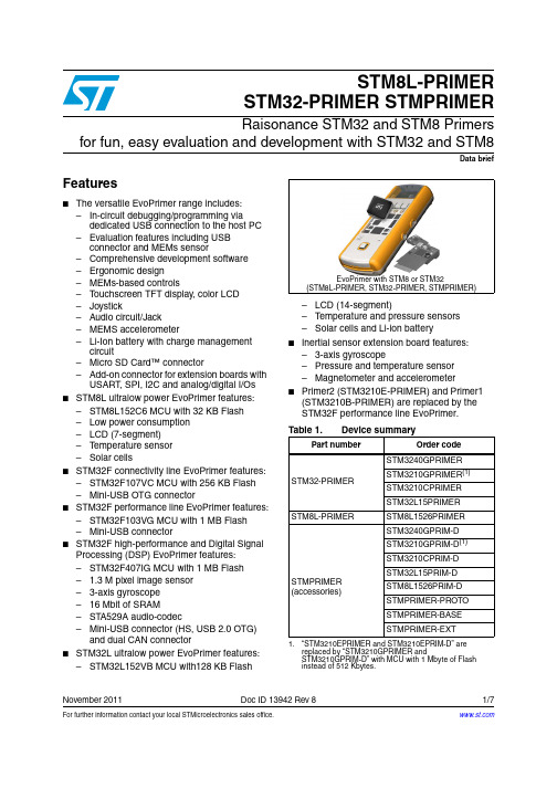
STM8超低功耗微控制器平台低功耗的承诺●从STM8L到STM32L完整的低功耗微控制器平台●采用最新、超低漏电流的工艺●极大的改善包括动态和静态的功耗高效率的承诺●由于采用最新的架构,性能/功耗比达到新高●运行模式功耗低至:150 μA/MHz●在低功耗模式下,仅需350nA,SRAM和寄存器数据还可以保留优化的产品分布●采用通用单片机从8位到32位全覆盖的策略●针对特殊的应用,提供片上集成的安全特性●最佳的性价比低功耗的要点超低功耗130nm工艺●在全温度范围内超低漏电流,工作电压低至1.8V.●性能和功耗与工作电压密切相关的。
低功耗设计●自动时钟门控●带有自动进入低功耗功能的闪存●DAC 和ADC工作电压低至1.8V●闪存编程电压可低至1.65V低功耗模式●多种低功耗模式:低功耗运行模式,低功耗等待模式,活跃暂停模式,暂停模式低至0.35μA●低功耗模式快速启动–暂停模式启动为4μs低功耗时钟●内部RC振荡器优化后在2MHz启动,以降低功耗●内部36.768KHz振荡器校正可达+/-0.2% ,以减少外部晶振的功耗STM8L 特性●采用高性能STM8 8位内核:在16Mhz运行频率下,高达16MIPS●26个引脚和软件兼容的型号,3个产品线●内置4KB 到32KB Flash,多达2KB SRAM●在运行模式下,功耗低至150 μA/MHz●提供四种低功耗模式,在SRAM数据保留的低功耗模式下,功耗仅为350 nA ●配置丰富的数字和模拟外设●提供免费的触摸感应程序库STM8L 电源监控和复位电路●电源监控和复位电路Full Reset circuitry / Supply Monitoring上电复位/掉电复位"零功耗"—一直打开电源下降检测—BOR 在低功耗模式可以被打开或关闭可编程电压检测—可以被打开或关闭在BOR关闭的情况下,电池电压低至1.65V, STM8L 依然可以工作●在运行模式下,用户通过选项字节激活BOR.●BOR 工作对电源电压上升/下降的时间没有特别的要求,也就意味着对电源波形没有特别的要求STM8L 灵活的时钟控制器●时钟失效监测和恢复机制●内部高速RC振荡器(HSI) @16MHz, 在室温下最大+/-2%误差●内部32.768KHz晶振时钟源,可自我校正到+/-0.2% 的精度●内部低速RC振荡器(LSI) 32KHz,带有自动唤醒功能。


STM参考手册中文pdf23 串行外设接口(SPI)小容量产品是指闪存存储器容量在16K至32K字节之间的STM32F101xx、STM32F102xx和STM32F103xx微控制器。
中容量产品是指闪存存储器容量在64K至128K字节之间的STM32F101xx、STM32F102xx和STM32F103xx微控制器。
大容量产品是指闪存存储器容量在256K至512K字节之间的STM32F101xx和STM32F103xx微控制器。
互联型产品是指STM32F105xx和STM32F107xx微控制器。
除非特别说明,本章描述的模块适用于整个STM32F10xxx微控制器系列。
SPI简介在大容量产品和互联型产品上,SPI接口可以配置为支持SPI协议或者支持I2S音频协议。
SPI接口默认工作在SPI方式,可以通过软件把功能从SPI 模式切换到I2S模式。
在小容量和中容量产品上,不支持I2S音频协议。
串行外设接口(SPI)允许芯片与外部设备以半/全双工、同步、串行方式通信。
此接口可以被配置成主模式,并为外部从设备提供通信时钟(SCK)。
接口还能以多主配置方式工作。
它可用于多种用途,包括使用一条双向数据线的双线单工同步传输,还可使用CRC校验的可靠通信。
I2S也是一种3引脚的同步串行接口通讯协议。
它支持四种音频标准,包括飞利浦I2S标准,MSB和LSB对齐标准,以及PCM标准。
它在半双工通讯中,可以工作在主和从2种模式下。
当它作为主设备时,通过接口向外部的从设备提供时钟信号。
警告:由于SPI3/I2S3的部分引脚与JTAG引脚共享(SPI3_NSS/I2S3_WS与JTDI,SPI3_SCK/I2S3_CK与JTDO),因此这些引脚不受IO控制器控制,他们(在每次复位后)被默认保留为JTAG用途。
如果用户想把引脚配置给SPI3/I2S3,必须(在调试时)关闭JTAG并切换至SWD接口,或者(在标准应用时)同时关闭JTAG和SWD接口。
UM0560User manualSTM8 bootloader 1 IntroductionThis document describes the features and operation of the STM8 integrated bootloaderprogram. This code embedded in the system memory of the device (ROM memory allowsmemories, including Flash program, data EEPROM, and RAM, to be written into the deviceusing the standard serial interfaces LINUART/UART/USART, SPI, and CAN.The bootloader code is similar for all STM8 versions. However, even though a peripheralmay be present in a product, the product may not support it (for example the SPI is notsupported in 128 Kbyte devices. In addition, different STM8 device types support differentperipherals (see Table5: Serial interfaces associated with STM8 devices for detailedinformation.For further information on the STM8 family features, pinout, electrical characteristics,mechanical data and ordering information, please refer to the STM8 datasheets.March 2011Doc ID 14798 Rev 41/70Contents UM0560Contents1Introduction . . . . . . . . . . . . . . . . . . . . . . . . . . . . . . . . . . . . . . . . . . . . . . . . 12Bootloader introduction . . . . . . . . . . . . . . . . . . . . . . . . . . . . . . . . . . . . . . 62.1Bootloader activation . . . . . . . . . . . . . . . . . . . . . . . . . . . . . . . . . . . . . . . . . 73Peripheral settings . . . . . . . . . . . . . . . . . . . . . . . . . . . . . . . . . . . . . . . . . 113.1USART/UARTs settings . . . . . . . . . . . . . . . . . . . . . . . . . . . . . . . . . . . . . . 11 3.1.1LINUART/UARTs in “reply” mode settings . . . . . . . . . . . . . . . . . . . . . . . 11 3.2SPI settings . . . . . . . . . . . . . . . . . . . . . . . . . . . . . . . . . . . . . . . . . . . . . . . 123.3CAN settings . . . . . . . . . . . . . . . . . . . . . . . . . . . . . . . . . . . . . . . . . . . . . . 134Bootloader command set . . . . . . . . . . . . . . . . . . . . . . . . . . . . . . . . . . . . 144.1Get command . . . . . . . . . . . . . . . . . . . . . . . . . . . . . . . . . . . . . . . . . . . . . . 154.1.1Get command via USART/LINUART/UART1/ UART2/UART3 . . . . . . . . 15 4.1.2Get command via SPI . . . . . . . . . . . . . . . . . . . . . . . . . . . . . . . . . . . . . . 174.1.3Get command via CAN . . . . . . . . . . . . . . . . . . . . . . . . . . . . . . . . . . . . . 194.2Read memory command . . . . . . . . . . . . . . . . . . . . . . . . . . . . . . . . . . . . . 214.2.1Read memory command via USART/LINUART/UART1/UART2/UART3 214.2.2Read memory command via SPI . . . . . . . . . . . . . . . . . . . . . . . . . . . . . . 234.2.3Read memory command via CAN . . . . . . . . . . . . . . . . . . . . . . . . . . . . . 264.3Erase memory command . . . . . . . . . . . . . . . . . . . . . . . . . . . . . . . . . . . . . 274.3.1Erase memory command via USART/LINUART/UART1/UART2/UART3 . . . . . . . . . . . . . . . . . . . . . . . . . . . . . . . . . . . . . . . . . . . . . . . . . . 284.3.2Erase memory command via SPI . . . . . . . . . . . . . . . . . . . . . . . . . . . . . 314.3.3Erase memory command via CAN . . . . . . . . . . . . . . . . . . . . . . . . . . . . 334.4Write memory command . . . . . . . . . . . . . . . . . . . . . . . . . . . . . . . . . . . . . 354.4.1Write memory command via USART/LINUART/UART1/UART2/UART3 364.4.2Write memory command via SPI . . . . . . . . . . . . . . . . . . . . . . . . . . . . . . 384.4.3Write memory command via CAN . . . . . . . . . . . . . . . . . . . . . . . . . . . . . 414.5Speed command . . . . . . . . . . . . . . . . . . . . . . . . . . . . . . . . . . . . . . . . . . . 434.5.1Speed command via CAN . . . . . . . . . . . . . . . . . . . . . . . . . . . . . . . . . . . 434.6Go command . . . . . . . . . . . . . . . . . . . . . . . . . . . . . . . . . . . . . . . . . . . . . . 454.6.1Go command via USART/LINUART/UART1/UART2/UART3 . . . . . . . . . 454.6.2Go command via SPI . . . . . . . . . . . . . . . . . . . . . . . . . . . . . . . . . . . . . . . 472/70Doc ID 14798 Rev 4UM0560Contents4.6.3Go command via CAN . . . . . . . . . . . . . . . . . . . . . . . . . . . . . . . . . . . . . . 494.7Sector codes . . . . . . . . . . . . . . . . . . . . . . . . . . . . . . . . . . . . . . . . . . . . . . 504.8Software model (STM8A/L/S . . . . . . . . . . . . . . . . . . . . . . . . . . . . . . . . . . 564.8.1RAM erase/write routines . . . . . . . . . . . . . . . . . . . . . . . . . . . . . . . . . . . 575Error management . . . . . . . . . . . . . . . . . . . . . . . . . . . . . . . . . . . . . . . . . 586Programming time . . . . . . . . . . . . . . . . . . . . . . . . . . . . . . . . . . . . . . . . . . 59Appendix A How to upload ROP protected device . . . . . . . . . . . . . . . . . . . . . . . 60A.1Rules for upgrading ROP protected devices. . . . . . . . . . . . . . . . . . . . . . . 60 Appendix B Bootloader entry points . . . . . . . . . . . . . . . . . . . . . . . . . . . . . . . . . . 61Appendix C SPI peripheral timing options. . . . . . . . . . . . . . . . . . . . . . . . . . . . . . 62C.1SPI with busy state checking. . . . . . . . . . . . . . . . . . . . . . . . . . . . . . . . . . . 62C.2Modified erase/write RAM routines. . . . . . . . . . . . . . . . . . . . . . . . . . . . . . 62 Appendix D PC software support . . . . . . . . . . . . . . . . . . . . . . . . . . . . . . . . . . . . . 63Appendix E Bootloader UART limitation . . . . . . . . . . . . . . . . . . . . . . . . . . . . . . . 64E.1Description . . . . . . . . . . . . . . . . . . . . . . . . . . . . . . . . . . . . . . . . . . . . . . . . 64E.1.1UART automatic baudrate calculation. . . . . . . . . . . . . . . . . . . . . . . . . . . 64E.1.2Description of UART limitation . . . . . . . . . . . . . . . . . . . . . . . . . . . . . . . . 64E.2Workaround for UART limitation . . . . . . . . . . . . . . . . . . . . . . . . . . . . . . . . 65 Appendix F Limitations and improvements versus bootloader versions. . . . . 66 Revision history . . . . . . . . . . . . . . . . . . . . . . . . . . . . . . . . . . . . . . . . . . . . . . . . . . . . 68Doc ID 14798 Rev 43/70List of tables UM0560 List of tablesTable 1.STM8 subfamilies featuring abootloader. . . . . . . . . . . . . . . . . . . . . . . . . . . . . . . . . . . . . . . 6 Table 2. STM8 subfamilies without bootloader . . . . . . . . . . . . . . . . . . . . . . . . . . . . . . . . . . . . . . . . . 7 Table3.Bootloader versions for which bootloader activation flowchart isvalid. . . . . . . . . . . . . . . . . 7 Table 4.Initialchecking . . . . . . . . . . . . . . . . . . . . . . . . . . . . . . . . . . . . . . . . . . . . . . . . . . . . . . . . . . 10 Table 5.Serial interfaces associated with STM8devices. . . . . . . . . . . . . . . . . . . . . . . . . . . . . . . . . 11 Table 6.Bootloadercommands . . . . . . . . . . . . . . . . . . . . . . . . . . . . . . . . . . . . . . . . . . . . . . . . . . . . 14 Table 7.Bootloader codes . . . . . . . . . . . . . . . . . . . . . . . . . . . . . . . . . . . . . . . . . . . . . . . . . . . . . . . .14 Table 8.Examples ofdelay . . . . . . . . . . . . . . . . . . . . . . . . . . . . . . . . . . . . . . . . . . . . . . . . . . . . . . . 39 Table9.STM8 sector codes. . . . . . . . . . . . . . . . . . . . . . . . . . . . . . . . . . . . . . . . . . . . . . . . . . . . . . .50 Table 10.Errortable. . . . . . . . . . . . . . . . . . . . . . . . . . . . . . . . . . . . . . . . . . . . . . . . . . . . . . . . . . . . . . 58 Table ART/LINUART/UART1/UART2/UART3 programmingtimes. . . . . . . . . . . . . . . . . . . . . 59 Table 12.SPI programmingtime . . . . . . . . . . . . . . . . . . . . . . . . . . . . . . . . . . . . . . . . . . . . . . . . . . . . 59 Table 13.CAN programming time . . . . . . . . . . . . . . . . . . . . . . . . . . . . . . . . . . . . . . . . . . . . . . . . . . . 59 Table 14.Bootloader entrypoints. . . . . . . . . . . . . . . . . . . . . . . . . . . . . . . . . . . . . . . . . . . . . . . . . . . . 61 Table15.Description of limitation, improvements and addedfeatures . . . . . . . . . . . . . . . . . . . . . . . 66 Table 16.Document revisionhistory . . . . . . . . . . . . . . . . . . . . . . . . . . . . . . . . . . . . . . . . . . . . . . . . . 68 4/70Doc ID 14798 Rev 4UM0560List of figures List of figuresFigure 1.Bootloader activation flowchart . . . . . . . . . . . . . . . . . . . . . . . . . . . . . . . . . . . . . . . . . . . . . . 8 Figure 2.CANframe . . . . . . . . . . . . . . . . . . . . . . . . . . . . . . . . . . . . . . . . . . . . . . . . . . . . . . . . . . . . . 13 Figure 3.Get command via USART/LINUART/UART1/UART2/UART3 - hostside . . . . . . . . . . . . . 15 Figure 4.Get command viaUSART/LINUART/UART1/UART2/UART3 - device side. . . . . . . . . . . . 16 Figure5.Get command via SPI - host side. . . . . . . . . . . . . . . . . . . . . . . . . . . . . . . . . . . . . . . . . . . .17 Figure 6.Get command via SPI - deviceside . . . . . . . . . . . . . . . . . . . . . . . . . . . . . . . . . . . . . . . . . . 18 Figure 7.Get command via CAN - host side. . . . . . . . . . . . . . . . . . . . . . . . . . . . . . . . . . . . . . . . . . . 19 Figure 8.Get command via CAN - device side . . . . . . . . . . . . . . . . . . . . . . . . . . . . . . . . . . . . . . . . . 20 Figure 9.Read memory command via USART/LINUART/UART1/UART2/UART3 - host side. . . . . 21 Figure 10.Read memory command viaUSART/LINUART/UART1/UART2/UART3 - device side . . . 22 Figure 11.Read memory command via SPI - host side . . . . . . . . . . . . . . . . . . . . . . . . . . . . . . . . . . . 23 Figure 12.Read memory command via SPI - deviceside. . . . . . . . . . . . . . . . . . . . . . . . . . . . . . . . . . 25 Figure 13.Read memory command via CAN - host side. . . . . . . . . . . . . . . . . . . . . . . . . . . . . . . . . . . 26 Figure 14.Read memory command via CAN - device side. . . . . . . . . . . . . . . . . . . . . . . . . . . . . . . . . 26 Figure 15.Erase memory command via USART/LINUART/UART1/UART2/UART3 - host side. . . . . 28 Figure 16.Erase memory command viaUSART/LINUART/UART1/UART2/UART3 - device side. . . 30 Figure 17.Erase memory command via SPI - host side . . . . . . . . . . . . . . . . . . . . . . . . . . . . . . . . . . . 31 Figure 18.Erase memory command via SPI - deviceside . . . . . . . . . . . . . . . . . . . . . . . . . . . . . . . . . 32 Figure 19.Erase memory command via CAN - host side . . . . . . . . . . . . . . . . . . . . . . . . . . . . . . . . . . 33 Figure 20.Erase memory command via CAN - device side . . . . . . . . . . . . . . . . . . . . . . . . . . . . . . . . 34 Figure 21.Write memory command via USART/LINUART/UART1/UART2/UART3 - hostside . . . . . 36 Figure 22.Write memory command viaUSART/LINUART/UART1/UART2/UART3 - device side . . . 37 Figure 23.Write memory command via SPI - host side. . . . . . . . . . . . . . . . . . . . . . . . . . . . . . . . . . . . 38 Figure 24.Write memory command via SPI - deviceside. . . . . . . . . . . . . . . . . . . . . . . . . . . . . . . . . . 40 Figure 25.Write memory command via CAN - host side. . . . . . . . . . . . . . . . . . . . . . . . . . . . . . . . . . . 41 Figure 26.Write memory command via CAN - device side. . . . . . . . . . . . . . . . . . . . . . . . . . . . . . . . . 42 Figure 27.Speed command via CAN - hostside. . . . . . . . . . . . . . . . . . . . . . . . . . . . . . . . . . . . . . . . . 43 Figure 28.Speed command via CAN - device side. . . . . . . . . . . . . . . . . . . . . . . . . . . . . . . . . . . . . . . 44 Figure 29.Go command via USART/LINUART/UART1/UART2/UART3 - host side. . . . . . . . . . . . . .45 Figure 30.Go command via USART/LINUART/UART1/UART2/UART3 - device side . . . . . . . . . . . . 46 Figure 31.Go command via SPI - hostside . . . . . . . . . . . . . . . . . . . . . . . . . . . . . . . . . . . . . . . . . . . . 47 Figure 32.Go command via SPI - device side. . . . . . . . . . . . . . . . . . . . . . . . . . . . . . . . . . . . . . . . . . . 48 Figure 33.Go command via CAN - hostside . . . . . . . . . . . . . . . . . . . . . . . . . . . . . . . . . . . . . . . . . . . 49 Figure 34.Go command via CAN - device side. . . . . . . . . . . . . . . . . . . . . . . . . . . . . . . . . . . . . . . . . . 49 Figure35.Delay elimination in modified RAMroutines . . . . . . . . . . . . . . . . . . . . . . . . . . . . . . . . . . . 62 Figure 36."Flash loader demonstrator" software. . . . . . . . . . . . . . . . . . . . . . . . . . . . . . . . . . . . . . . . . 63Doc ID 14798 Rev 45/706/70Doc ID 14798 Rev 42 Bootloader introductionThe main task of the bootloader is to download the application program into the internalmemories through the integrated peripherals (UARTs, SPI, or CAN without using the SWIM protocol and dedicated hardware. Data are provided by any device (host which is capable of sending information through one of the above-mentioned serial interfaces.The bootloader permits downloading of application software into the device memories, including RAM, program and data memory, using standard serial interfaces. It is a complementary solution to programming via the SWIM debugging interface.The bootloader code is stored in the internal boot ROM memory. After a reset, thebootloader code checks whether the program memory is virgin or whether a specific option byte is set allowing code modifications.If these conditions are not fulfilled, the bootloader resumes and the user application is started.In case of a successful check the bootloader is executed.When the bootloader procedure starts, the main tasks are:●Polling all supported serial interfaces to check which peripheral is used●Programming code, data, option bytes and/or vector tables at the address(es received from the host.Each STM8 device embeds a specific bootloader code which is common to a whole group of STM8 devices. The correspondence between STM8 groups and STM8 part numbers is given in Table 1. Group names are used all over this user manual.Table 2 gives the list of STM8 devices without embedded bootloader (no ROM bootloader is implemented inside the microcontroller. When using these devices, youhave to write your own bootloader code and save it in the UBC program area (refer to STM8S and STM8A families reference manual for information on the UBC area.Table 1.STM8 subfamilies featuring a bootloaderSTM8 group STM8 part numbersSTM8A/S-128KSTM8AF52xx, STM8AF6269/8x/Ax, STM8AF51xx, STM8AF6169/7x/8x/9x/Ax,STM8S20xxx STM8A/S-32KSTM8AF622x/4x, STM8AF6266/68, STM8AF612x/4x, STM8AF6166/68,STM8S105xxSTM8L-64k STM8L15xx8, STM8L15xR6, STM8L16xx8STM8L-32KSTM8L15xC4, STM8L15xK4, STM8L15xG4,STM8L15xC6, STM8L15xK6, STM8L15xG6(x = 1 or 2STM8L-8KSTM8L15xC2, STM8L15xK2, STM8L15xG2, STM8L15xC3, STM8L15xK3, STM8L15xG3(x = 1 or 2Doc ID 14798 Rev 47/702.1 Bootloader activationThe STM8 hardware reset vector is located at the beginning of the boot ROM(0x006000,while the other interrupt vectors are in the Flash program memory starting at address 0x008004.The device executes the boot ROM (jumps inside the boot ROM area and after checking certain address locations (see Table 4: Initial checking on page 10, it starts to execute the bootloader or the user code defined by the reset vector (0x008000.The bootloader activation flowchart is described in Figure 1: Bootloader activation flowchart . In previous bootloader versions, a return to the “wait for SYNCHR” state (see dashed line in Figure 1 was performed when the “Flash virgin” test was positive. In newer versions, it has been replaced by a software (SW reset to prevent the customer firmware from remaining in a infinite loop (e.g. due to EMC disturbance. This bootloader modification is referred to as "EMC lockup protection" in T able 15. Table 3 lists the bootloader versions for which the dashed line was replaced by a SW reset.The bootloader version number of a given device is obtained by the “Get command” (see Section 4.1: Get command . The bootloader version is represented by a two-digitbinary-coded decimal (BCD number (with a decimal point between the two digits which is coded into one byte in the “Get command” result. For example, 0x21 version byte is bootloader version 2.1.Table 2.STM8 subfamilies without bootloaderSTM8 group STM8 part numbersSTM8A/S-8K STM8Sx03xx STM8L-8KSTM8L101xxTable 3.Bootloader versions for which bootloader activation flowchart is validSTM8 group Bootloader versionSTM8A/S-128K v2.2STM8A/S-32K v1.3STM8L-64K v1.0STM8L-32K v1.2STM8L-8Kv1.01.See Flow chart description on page9 for explanation of points 1 to 8.2.See Table4: Initial checking.3.Dotted routines are loaded in RAM by the host. They are removed by the go command before jumping to the Flash programmemory to execute an application.8/70Doc ID 14798 Rev 4Flow chart description1.Disable all interrupt sources.2. The host can start the bootloader process according to checks shown in Table4 (inkeeping with the content of the first Flash program memory location (0x008000 and “bootloader enable” option bytes. The host checks the following bootloader startconditions:Condition 1: the host checks if the device memory is empty by inspecting the content of address 0x00 8000 (reset vector. If the content is not equal to 0x82 or 0xAC, thedevice is recognized as being empty and the bootloader remains active and waits for host commands without timeouts.Condition 2: the host checks if the bootloader option bytes (two bytes are set to enable the bootloader or not. The bootloader is enabled with a value of 0x55AA and disabled by all other values (see the device datasheets for the bootloader option byte locations.If the option bytes are enabled, the bootloader remains active and waits for hostcommands with a 1-second timeout. If the host does not send a command within this timeout, the bootloader jumps directly to the application user vector (jump to address0x008000.Condition 3: If the option bytes disable the bootloader (by a value different from0x55AA, the bootloader jumps directly to the application user vector (jump to address 0x00 8000.The above checking process is summarized in T able4.3. When readout protection (ROP is active, the Flash program memory is readoutprotected. In this case, the bootloader stops and the user application starts. If ROP is inactive, the bootloader continues to be executed (see Appendix A: How to upload ROP protected device.4. The CAN peripheral can only be used if an external clock (8 MHz, 16 MHz, or 24 MHzis present. It is initialized at 125 kbps. The UARTs and SPI peripherals do not require an external clock.5. Set the high speed internal RC oscillator (HSI to 16 MHz and initialize the UARTsreceiver pins in input pull-up mode in the GPIO registers. Initialize the SPI in slave mode. Then, wait 4 ms for I/O pin voltage level stabilization. It is recommended that the host waits 10 ms from the STM8 reset before sending the SYNCHR byte/message.This is the time needed for bootloader initialization.Doc ID 14798 Rev 49/7010/70Doc ID 14798 Rev 46.Interface polling: The bootloader polls all peripherals waiting for a synchronizationbyte/message (SYNCHR = 0x7F within a timeout of 1 s. If a timeout occurs, either the Flash program memory is virgin in which case it waits for a synchronizationbyte/message in an infinite loop through a software reset, or the Flash programmemory is not virgin and the bootloader re stores the registers’ reset status and jumps to the memory address given by the reset vector (located at 0x008000. For thebootloader versions listed in Table 3, a software reset is generated after a timeout has elapsed, in case the Flash program memory is empty (this is because it is safer to stay in an infinite loop if there is a hardware chip error.Note:When synchronization fails (the bootloader receives a byte/message different to‘SYNCHR’ = 0x7F two different situations can be distinguished according to the peripheral:With the UART peripherals, a device reset or power-down is necessary beforesynchronization can be tried again. Refer to Appendix E: Bootloader UART limitation With the CAN or SPI peripheral, the user can continue to poll the interfaces until a synchronization or a timeout occurs.7.If the synchronization message is received by the UARTs, the bootloader automatically detects the baud rate, initializes the UART and goes to step 8 below. If thesynchronization message is received by the CAN or SPI, the bootloader goes directly to step 8 below.Note: Once one of the available interfaces receives the synchronization message, all others are disabled.8.Waiting for commands: Commands are checked in an infinite loop and executed. To exit from the bootloader, the host has to send a ‘GO’ command. When this is done, the bootloader removes the EM and WM routines from the RAM memory and jumps to the address selected by the host.Note:To be able to write/erase data in Flash and EEPROM the host must write into RAMexecutable routines for writing and erasing. Those routines (*.s19 files are provided with the bootloader. Host must upload those routines at address 0xA0. See section 4.8.1: RAM erase/write routines for more information.Note:After interface initialization, the ROP bit is checked to avoid non-authorized reading of the Flash program memory and data EEPROM.Table 4.Initial checkingChecksProgram memory byte location [0x008000]Bootloader check option bytes[BL_OPT](11.See device datasheet for the [BL_OPT] location in the option byte area memory map.Actual Flash program memory status-> Flash action1st [0x00 8000] <>(0x82 or 0xAC[BL_OPT] = 0x00XXXX Flash program memory virgin.-> jump to bootloader 2nd[0x00 8000] <>(0x82 or 0xAC[BL_OPT] = 0x0055AA Flash program memory already written, bootloader enabled by option bytes.-> jump to bootloader 3rd[0x00 8000] <>(0x82 or 0xAC[BL_OPT] <> 0x0055AAFlash program memory already written,bootloader disabled by option bytes.-> jump to Flash program memory resetUM0560Peripheral settingsDoc ID 14798 Rev 411/703 Peripheral settingsThis section describes the hardware settings of the STM8 communication peripherals:●UARTs/LINUART ●SPI ●CANNote:During bootloading only one peripheral (first addressed is enabled. All others are disabled.3.1 USART/UARTs settingsThis peripheral supports asynchronous serial communication.The USART/UARTs settings are:●Data frame: 1 start bit, 8 data bit, 1 parity bit set to even, 1 stop bit●Baud rate: The baud rate is automatically detected by the bootloader. When the usersends the synchronization byte, 0x7F , the bootloader automatically detects the baud rate and sets the USART/UARTs to the same baud rate. Maximum baud rate = 1 Mbps (115200 baud for STM8L-64K; minimum baud rate = 4800 bps.To perform the automatic speed detection, the RxD line must be stable in the application board (internal pull-up is enabled on the RxD line by the bootloader.3.1.1 LINUART/UARTs in “reply” mode settingsSettings are:●Data frame: 1 start bit, 8 data bit, no parity bit, 1 stop bit●Baud rate: The baud rate is automatically detected by the bootloader. When the user sends the synchronization byte 0x7F , the bootloader automatically detects the baud rate and sets the UARTs to the same baud rate. Maximum baud rate = 550 kbps (115200 baud for STM8L-64K; minimum baud rate = 4800 bps.To perform automatic speed detection, the RxD line must be stable in the application board (internal pull-up is enabled on the RxD line by the bootloader.Table 5.Serial interfaces associated with STM8 devices (11.The above table reflects only current bootloader versions and device states.STM8 groups Serial interfaceSTM8A-128K USART , LINUART (in “reply” mode, CAN STM8A-32K LINUART, SPISTM8S-128K UART1, UAR T3 (in “reply” mode, CAN STM8S-32K UART2 (in “reply” mode, SPI STM8L-8K UART, SPI STM8L-32K UARTSTM8L-64KUART1, UART2, UART3 (in “reply” mode,SPI1, SPI2Peripheral settings UM056012/70Doc ID 14798 Rev 4Reply modeThe host must reply to all the bytes sent from the bootloader. If TxD and RxD lines share the same physical medium (for example, 1-wire communication, then host replies are not necessary since RxD and TxD pins coincide.3.2 SPI settingsThe SPI settings are:●8 data bit, MSB first●Bit rate: S et by the host which acts as a master●Peripheral set in slave mode with software management of NSS●Data polarity : CPOL = 0 (SCK to 0 when idle, CPHA = 0 (the first clock transition is thefirst data capture edge.Note:1Before sending a ‘token’ byte, th e host has to wait for a delay of a specified period of time. If this period is not quantified, it is equal to 6 µs.2The SPI peripheral is accessible via SPI_SCK, SPI_MOSI and SPI_MISO pins.UM0560Peripheral settingsDoc ID 14798 Rev 413/703.3 CAN settingsTo address additional devices on the same bus, the CAN protocol provides a standardidentifier field (11-bit and an optional extended identifier field (18-bit in the frame. Figure 2 shows the CAN frame that uses the standard identifier only.The CAN settings are as follows:●Standard identifier (not extended●Bit rateBy default, it is 125 kbps. The runtime can be changed via the speed command to achieve a maximum bitrate of 1 Mbps.The transmit settings (from the STM8 to the host are:●Tx mailbox0: On●Tx mailbox1 and Tx mailbox2: Off ●Tx identifier: 0x02●Outgoing messages contain 1 data byteThe receive settings (from the host to the STM8 are:●The synchronization byte, 0x7F , is in the RX identifier and not in the data field●The RX identifier depends on the command (0x00, 0x03, 0x11, 0x21, 0x31, 0x43●Error checking: If the error field (bit [6:4] in the CESR register is different from 000b, the message is discarded and a NACK is sent to the host.●In FIFO overrun condition, the message is discarde d and a NACK is sent to the host.●Incoming messages can contain from 1 to 8 data bytes.Note:The CAN peripheral is accessible via CAN_TX and CAN_RX pins.Bootloader command set UM056014/70Doc ID 14798 Rev 44 Bootloader command setThe commands supported by the bootloader are listed in Table 6 below.Table 7.Bootloader codesWhen the bootloader receives a command via the UARTs, CAN or SPI peripherals, the general protocol is as follows:1.The bootloader sends an ACK byte (0x79 to the host and waits for an address and for a checksum byte, both of which are checked when received.2.When the address is valid and the checksum is correct, the bootloader transmits an ACK byte (0x79, otherwise it transmits a NACK byte (0x1F and aborts the command. The bootloader waits for the number of bytes to be transmitted (N bytes and for its complemented byte (checksum. –If the checksum is correct, it then carries out the command, starting from the received address.–If the checksum is incorrect, it sends a NACK (0x1F byte before aborting the command.Table 6.Bootloader commandsCommandCommand codeCommand descriptionGet 0x00Gets the version and the allowed commands supported bythe current version of the bootloaderRead memory 0x11Reads up to 256 bytes of memory starting from an address specified by the hostErase memory0x43Erases from one to all of the Flash program memory/data EEPROM sectorsWrite memory0x31Writes up to 128 bytes to RAM or the Flash programmemory/data EEPROM starting from an address specified by the hostSpeed 0x03Allows the baud rate for CAN runtime to be changed Go0x21。

UM0970用户手册STM8L-DISCOVERY 简介STM8L-DISCOVERY可以帮助用户探索发现STM8L的超低功耗特性,也可以开发相关的应用。
STM8L-DISCOVERY是基于STM8L152C6T6芯片做的开发板,包括一个嵌入的ST-LINK调试工具接口(ST-LINK调试器/编程器集成在同一块板子上,留有SWIM调试接口)、LCD(24段,4个COM 端)和按键。
图 1STM8L-DISCOVERY板本文仅供参考,请以ST官方文档为准/internet/com/TECHNICAL_RESOURCES/TECHNICAL_LITERATURE/USER_MANUAL/CD00278045.pdf目 录第1章 快速入门 (4)1.1 开始 (4)1.2 系统要求 (4)1.3 开发工具 (5)1.4 演示软件 (5)1.5 订单编码 (5)第2章 特点 (6)第3章 硬件和布局 (7)3.1 STM8L152C6T6微控制器 (11)3.2 嵌入的ST-LINK (13)3.2.1 使用ST-LINK编程/调试板上STM8L (14)3.2.2 使用ST-LINK编程/调试外部STM8L应用 (14)3.3 供电和电源选择 (15)3.4 LED灯 (15)3.5 按键 (16)3.6 内建的IDD测量电路 (16)3.6.1 运行模式 (17)3.6.2 低功耗模式 (17)3.6.3 低功耗模式IDD测量原理 (17)3.6.4 Ibias电流测量步骤 (18)3.7 锡桥 (18)3.8 LCD(24段,4个COM) (19)第4章 扩展连接 (22)第5章 机械制图 (26)第6章 电气原理图 (28)2 - 王志杰(QQ:411238869; MSN:iewangzhijie@)Design a Solution for Future第1章快速入门第1章 快速入门STM8L-DISCOVERY是一个低成本的、易于使用的开发工具,可快速评估和开始一个STM8L超低功耗微控制器的开发。
手动开关手动开关没有自动切换为直接的但它提供给用户的切换事件时间的精确控制。
参照图20中的流程图。
1。
写使用系统时钟开关选择目标时钟源的8位值寄存器(clk_swr)。
然后swbsy位是由硬件,和目标源振荡器开始。
古老的时钟源继续驱动CPU和外设。
2。
该软件具有等到目标时钟源准备(稳定的)。
这是在clk_swcr寄存器和快捷旗由中断如果swien位设置显示。
3。
最终软件的作用是设置,在所选择的时间,在clk_swcr的赛文点寄存器来执行开关。
在手动和自动切换模式,旧的系统时钟源不会自动关闭的情况下是由其他模块(LSI混凝土可用于例如独立的看门狗驱动)。
时钟源可以关机使用在内部时钟寄存器的位(clk_ickcr)和外部时钟寄存器(clk_eckcr)。
如果时钟开关不因任何原因的工作,软件可以通过清除swbsy 标志复位电流开关操作。
这将恢复clk_swr注册到其以前的内容(旧的系统时钟)。
注意:在清理swbsy标志具有复位时钟主开关的程序,应用程序必须等到后产生新的主时钟切换请求之前有一段至少两个时钟周期。
9.7周门控时钟(PCG)外周时钟门控(PCG)模式选择性地启用或禁用系统时钟(SYSCLK)连接到外围设备在运行或慢速模式的任何时间来优化功耗。
设备复位后,所有的外设时钟被禁用。
唯一的一点是在复位状态是默认启用pcken27因为它用于启动。
软件已被正确地写入关掉ROM Bootloader执行后的时钟。
您可以启用时钟的任何外围设置在clk_pckenrx周围门控时钟寄存器的相应pcken点。
●使周围,首先使在clk_pckenr相应的pcken点寄存器然后设置使点周围的外围控制寄存器。
●禁用适当的外围,先禁用在周边的适当位控制寄存器,然后停止相应的时钟。
注:蜂鸣器,RTC和液晶显示器是由不同的SYSCLK特定的时钟,使他们继续运行,即使时钟门控的外设寄存器是断言。
9.8时钟安全系统(CSS)9.8.1时钟安全系统对HSE时钟安全系统(CSS)监控HSE晶体时钟源故障时安全作为系统时钟。
本参考手册的目标应用程序开发人员。
它提供了完整的信息如何使用stm8l05xx,stm8l15xx和stm8l16xx微控制器的存储器和外围设备。
该stm8l05xx / stm8l15xx / stm8l16xx是一个家庭的不同存储密度的微控制器和外围设备。
这些产品是专为超低功耗应用。
可用的外设的完整列表,请参阅产品数据表。
订购信息,引脚说明,机械和电气设备的特点,请参阅产品数据表。
关于STM8 SWIM通信协议信息和调试模块,请参阅用户手册(um0470)。
在STM8的核心信息,请参阅STM8的CPU编程手册(pm0044)。
关于编程,擦除和保护的内部快闪记忆体,请参阅STM8L闪存编程手册(pm0054)。
1 中央处理单元(CPU)。
30。
1.1 引言301.2 CPU的寄存器。
30。
1.2.1 描述CPU寄存器。
..。
301.2.2 STM8 CPU寄存器图。
..。
341.3 全球配置寄存器(cfg_gcr)。
34。
1.3.1 激活水平。
..。
341.3.2 游泳禁用。
..。
351.3.3 描述全局配置寄存器(cfg_gcr)。
..。
351.3.4 全局配置寄存器图及复位值。
..。
352 启动ROM . . . 363程序存储器和数据存储器。
37。
3.1引言373.2术语。
37。
3.3个主要的快闪存储器的特点。
38。
3.4记忆的组织。
39。
3.4.1低密度设备的存储器组织。
393.4.2介质密度的装置记忆的组织。
..。
403.4.3介质+密度装置记忆的组织。
..。
413.4.4高密度存储器组织。
..。
423.4.5专有代码区(译)。
433.4.6用户区(UBC)。
433.4.7数据的EEPROM(数据)。
..。
463.4.8主程序区。
463.4.9选项字节。
..。
463.5内存保护。
47。
3.5.1读出保护。
473.5.2内存访问安全系统(质量)。
473.5.3使写访问选项字节。
493.6内存编程493.6.1同时读写(读写网)。
本参考手册的目标应用程序开发人员。
它提供了完整的信息如何使用stm8l05xx,stm8l15xx和stm8l16xx 微控制器的存储器和外围设备。
该stm8l05xx / stm8l15xx / stm8l16xx是一个家庭的不同存储密度的微控制器和外围设备。
这些产品是专为超低功耗应用。
可用的外设的完整列表,请参阅产品数据表。
订购信息,引脚说明,机械和电气设备的特点,请参阅产品数据表。
关于STM8 SWIM通信协议信息和调试模块,请参阅用户手册(um0470)。
在STM8的核心信息,请参阅STM8的CPU编程手册(pm0044)。
关于编程,擦除和保护的内部快闪记忆体,请参阅STM8L闪存编程手册(pm0054)。
1 中央处理单元(CPU)。
30。
1.1 引言301.2 CPU的寄存器。
30。
1.2.1 描述CPU寄存器。
..。
301.2.2 STM8 CPU寄存器图。
..。
341.3 全球配置寄存器(cfg_gcr)。
34。
1.3.1 激活水平。
..。
341.3.2 游泳禁用。
..。
351.3.3 描述全局配置寄存器(cfg_gcr)。
..。
35 1.3.4 全局配置寄存器图及复位值。
..。
352 启动ROM . . . 363程序存储器和数据存储器。
37。
3.1引言373.2术语。
37。
3.3个主要的快闪存储器的特点。
38。
3.4记忆的组织。
39。
3.4.1低密度设备的存储器组织。
393.4.2介质密度的装置记忆的组织。
..。
40 3.4.3介质+密度装置记忆的组织。
..。
41 3.4.4高密度存储器组织。
..。
423.4.5专有代码区(译)。
433.4.6用户区(UBC)。
433.4.7数据的EEPROM(数据)。
..。
463.4.8主程序区。
463.4.9选项字节。
..。
463.5内存保护。
47。
3.5.1读出保护。
473.5.2内存访问安全系统(质量)。
473.5.3使写访问选项字节。
20个16位通用定时器(TIM2,TIM3,tim5)20.1引言本章介绍TIM2,TIM3和tim5是相同的定时器。
每个定时器包括一个16位的升降自动重载计数器由一个可编程分频器驱动。
它可用于多种用途,包括:●时基产生●测量输入信号的脉冲长度(输入捕捉)●生成输出波形(输出比较,脉宽调制和脉冲模式)●中断能力的各种事件(捕获,比较,溢出)●同步与其他计时器或外部信号(外部时钟,复位,触发使)定时器时钟可以来自内部时钟可以通过配置寄存器或从外部源。
只有通用定时器的主要特点是本章中提出的。
指的是部分19:16点先进控制定时器对应的段落(TIM1)对每个功能的更多详细信息页面283。
20.2 TIMx主要特点通用TIMx TIM2 / TIM3功能包括:●16位上,下,上/ downauto刷新计数器。
●3位可编程分频器使计数器的时钟频率可分”飞”的任何权力,2从1到128。
2个独立的通道●:输入捕捉输出比较PWM生成(边缘对齐方式)-一个脉冲输出的方式●中断输入将定时器的输出信号在复位状态,或在一个已知状态。
●输入捕捉2可以通过从comp2比较器●中断和DMA请求生成下列事件:更新:计数器溢出时,计数器初始化(软件)输入捕捉输出比较中断输入触发事件(计数器的启动,停止,内部/外部触发初始化或计数)20.3.1时间单位计时器时基单元包括:●16位可逆计数器●16位自动重载寄存器●3位可编程分频器没有重复计数器。
时钟源是内部时钟(fsysclk)。
它是直接连接到ck_psc 时钟饲料的预分频器计数器的时钟ck_cnt驱动。
分频器分频器实现如下:●预分频器的基础上通过一个3位寄存器控制的7位计数器(在timx_pscr寄存器)。
它可以在飞这控制寄存器缓冲的改变。
它可以将计数器的时钟频率的1,2,4,8,16,32,64或128。
计数器的时钟频率计算如下:fck_cnt = fck_psc / 2(PSCR [2:0])计数器操作请参阅第19.3.4:上数288页,模式部分19.3.5:向下计数在290页和第19.3.6模式:中心对齐方式(向上/向下计数)292页。
STM8L中文参考手册(4)-
20 16位通用定时器(TIM2、TIM3、tim5)
20.1简介
本章介绍TIM2、TIM3和tim5是相同的定时器
每个定时器包括一个由可编程分频器驱动的16位上下自动重载计数器它可以用于多种目的,包括:●定时产生●测量输入信号的脉冲长度(输入捕获)
●产生输出波形(输出比较、脉宽调制和脉冲模式)●各种中断能力事件(捕获、比较、溢出)
●与其他定时器或外部信号(外部时钟、复位、触发使能)同步
定时器时钟可以来自内部时钟,也可以来自配置寄存器或外部源本章仅介绍通用定时器的主要特性。
它参考了与19:16高级控制定时器(TIM1)相对应的部分中的每个功能的更详细的信息页28320.2 TIMx 主要功能
通用TIMx TIM2/TIM3功能包括:
●16位向上、向下、向上/向下自动刷新计数器●3位可编程分频器允许将计数器的时钟频率分成1至128的任意2次方两个独立的低电平通道:输入捕获输出比较
脉冲宽度调制产生(边沿对齐)-一个脉冲输出模式
低电平中断输入,用于复位定时器输出信号,或处于已知状态●输入捕捉2可通过来自comp2比较器
:
更新的中断和DMA请求产生以下事件:当计数器溢出时,计数器初始化(软件)输入捕捉输出比较中断输入
触发事件(开始、停止、内部/外部触发初始化或计数)
20.3.1时间单元
定时器时基单元包括:●16位可逆计数器
时钟源是内部时钟(fsysclk)它由预分频器计数器的时钟ck_cnt驱动,预分频器计数器直接连接到ck_psc时钟馈送
分频器
分频器的实现如下:7位计数器(在timx_pscr寄存器中)由基于
低预分频器的3位寄存器控制它可以控制飞行中寄存器缓冲区的变化。
它可以将计数器的时钟频率转换为1、2、4、8、16、32、64或128计数器的时钟频率计算如下:
fCk _ CNT = fck _ PSC/2(PSCR[2:0)计数器操作
请参考第19.3.4页:上部288,模式部分19.3.5:在第290页向下计数,模式19.3.6:中心对齐(向上/向下计数)29220.3.2时钟/触发控制器
参见第296页第19.4节:TIM1时钟/触发控制器20.3.3采集/比较通道输入级
参见第310页第19.5节:TIM1采集/比较通道
有两个输入通道,如图122:输入级框图通道2内部连接到比较器
输出级
参见第19.5.4页:315,输出级19.5.5:强制输出模式在第316页,第19.5.7页:脉宽调制模式在第318页
如图124所示。
TIMx输出没有死区或互补输出当
使用中断功能中断
时,输出使能信号和无效电平根据附加控制位(timx_bkr寄存器中的MOE和Ossi位)进行修改当
退出复位时,中断电路被禁用,闪点低。
您可以通过设置timx_bkr 寄存器秘密位来中断该功能。
可以通过在同一寄存器中配置BKP点来选择中断输入极性贝克尔和BKP可以同时修改有关
的更多信息,请参见使用中断功能的-325页表73:具有销毁功能的OCI通道输出控制点(中断功能已实现,互补输出未实现)392页20.3.4定时器输入异或功能
在timx_cr2中注册ti1s位允许通道1的输入滤波器连接到异或门的输出,组合三个输入引脚timx_ch1、timx_ch2和timx_bkin
异或输出可用于所有输入功能,如触发或输入捕获
使用该功能作为接口的霍尔传感器的一个例子是19.5.12第331页的霍尔传感器接口。
20.4 TIMx中断
定时器5中断请求源:●捕获/比较2个中断●捕获/比较1个中断●更新中断●中断输入
●触发中断
使用中断功能设置timx_ier寄存器中所需的cc2ie和/或cc1ie位,为每个中断通道发出中断请求
不同的中断源也可以通过软件使用中相应的位寄存器产生timx_egr
7位:自动加载预载皮炎
0: TIMX _ ARR寄存器不通过预缓冲寄存器它可以通过预缓冲寄存器
位6: 5 CMS (1: 0):中心对齐选择
00:边缘对齐直接写入1: Timx _ ARR寄存器计数器计数的向上或向下方向取决于位(DIR)
01:中心对齐1计数器计数上下交替仅当计数器计数下降时,输出比较中断配置输出通道标志(CCIS = 00 timx_ccmri寄存器)
10:中心对齐2计数器计数上下交替仅当计数器计数时,输出比较中断配置输出通道标志(CCIS = 00 timx_ccmri寄存器)
11:中心对齐3计数器计数上下交替当计数器计数上升或下降时,设置输出比较中断配置输出通道标志(CCIS = 00 timx_ccmri寄存器)注意:只要启用计数器(Cen = 1),就不允许从边缘对齐切换到中心对齐在居中模式下,必须禁用
编码器模式(短消息= 001,010或011 gpt_smcr寄存器)4位控制器:direction
0:counter as counter 1:counter as counter
注意:如果定时器配置为中心对齐或编码模式,则该位为只读3位
OPM:单脉冲模式0:反连续更新事件
1:计数器在下一次更新事件时停止计数(结算中心点)2位策略:更新请求源
0:当启用udis点时,如果在发送点设置和更新中断请求时发生以下事件之一:寄存器更新(计数器上溢/下溢)-ug点由软件设置更新事件通过时钟/触发控制器1生成:当启用udis点时,如果仅当1位udis: update disable
0:当计数器溢出时,UEV产生时钟/触发模式控制器,或者产生更新软件或硬件复位缓冲寄存器,然后加载和预置值
1:不生成UEV,影子寄存器保持它们的值(ARR,PSC,中国棉花研究所)如果设置了UG位,计数器和分频器将重新初始化0记者:反击。