LM1117-3.3 电压转换芯片 数据手册 说明书
- 格式:pdf
- 大小:319.00 KB
- 文档页数:5
LM1117800mA Low-Dropout Linear RegulatorGeneral DescriptionThe LM1117is a series of low dropout voltage regulators with a dropout of1.2V at800mA of load current.It has the same pin-out as National Semiconductor’s industry standard LM317.The LM1117is available in an adjustable version,which can set the output voltage from1.25V to13.8V with only two ex-ternal resistors.In addition,it is also available in five fixed voltages,1.8V,2.5V,2.85V,3.3V,and5V.The LM1117offers current limiting and thermal shutdown.Its circuit includes a zener trimmed bandgap reference to as-sure output voltage accuracy to within±1%.The LM1117series is available in SOT-223,TO-220,and TO-252D-PAK packages.A minimum of10µF tantalum ca-pacitor is required at the output to improve the transient re-sponse and stability.Featuresn Available in1.8V,2.5V,2.85V,3.3V,5V,and Adjustable Versionsn Space Saving SOT-223Packagen Current Limiting and Thermal Protectionn Output Current800mA n Temperature Range0˚C to125˚C n Line Regulation0.2%(Max) n Load Regulation0.4%(Max)Applicationsn 2.85V Model for SCSI-2Active Terminationn Post Regulator for Switching DC/DC Convertern High Efficiency Linear Regulatorsn Battery Chargern Battery Powered InstrumentationTypical ApplicationActive Terminator for SCSI-2BusDS100919-5Fixed Output RegulatorDS100919-28LM1117 800mA Low-Dropout Linear RegulatorOrdering InformationPackageTemperature Range Packaging Marking Transport Media NSC Drawing 0˚C to +125˚C 3-lead SOT-223LM1117MPX-ADJN03A Tape and Reel MA04A LM1117MPX-1.8N12A Tape and Reel *LM1117MPX-2.5N13A Tape and Reel LM1117MPX-2.85N04A Tape and Reel LM1117MPX-3.3N05A Tape and Reel LM1117MPX-5.0N06A Tape and Reel 3-lead TO-220LM1117T-ADJLM1117T-ADJ Rails T03B LM1117T-2.85LM1117T-2.85Rails LM1117T-3.3LM1117T-3.3Rails LM1117T-5.0LM1117T-5.0Rails 3-lead TO-252LM1117DTX-ADJLM1117DT-ADJ Tape and Reel TD03BLM1117DTX-1.8LM1117DT-1.8Tape and Reel *LM1117DTX-2.5LM1117DT-2.5Tape and Reel LM1117DTX-2.85LM1117DT-2.85Tape and Reel LM1117DTX-3.3LM1117DT-3.3Tape and Reel LM1117DTX-5.0LM1117DT-5.0Tape and Reel Note:*Contact factory for availability.Block DiagramDS100919-1L M 1117Absolute Maximum Ratings (Note 1)If Military/Aerospace specified devices are required,please contact the National Semiconductor Sales Office/Distributors for availability and specifications.Maximum Input Voltage (V IN to GND)LM1117-ADJ,LM1117-1.8,LM1117-2.5,LM1117-3.3,LM1117-5.020V Power Dissipation (Note 2)Internally Limited Junction Temperature (T J )(Note 2)150˚C Storage Temperature Range-65˚C to 150˚C Lead Temperature TO-220(T)Package 260˚C,10sec SOT-223(IMP)Package 260˚C,4sec ESD Tolerance (Note 3)2000V Operating Ratings (Note 1)Input Voltage (V IN to GND)LM1117-ADJ,LM1117-1.8,LM1117-2.5,LM1117-3.3,LM1117-5.015V LM1117-2.8510V Junction Temperature Range (T J )(Note 2)0˚C to 125˚CElectrical CharacteristicsTypicals and limits appearing in normal type apply for T J =25˚C.Limits appearing in Boldface type apply over the entire junc-tion temperature range for operation,0˚C to 125˚C.SymbolParameter Conditions Min (Note 5)Typ (Note 4)Max (Note 5)Units V REF Reference Voltage LM1117-ADJI OUT =10mA,V IN -V OUT =2V,T J =25˚C10mA ≤I OUT ≤800mA,1.4V ≤V IN -V OUT≤10V1.2381.225 1.2501.250 1.2621.270V V V OUT Output Voltage LM1117-1.8I OUT =10mA,V IN =3.8V,T J =25˚C0≤I OUT ≤800mA,3.2V ≤V IN ≤10V1.7821.746 1.8001.800 1.8181.854V V LM1117-2.5I OUT =10mA,V IN =4.5V,T J =25˚C0≤I OUT ≤800mA,3.9V ≤V IN ≤10V2.4752.450 2.5002.500 2.5252.550V V LM1117-2.85I OUT =10mA,V IN =4.85V,T J =25˚C0≤I OUT ≤800mA,4.25V ≤V IN ≤10V0≤I OUT ≤500mA,V IN =4.10V2.8202.7902.790 2.8502.8502.850 2.8802.9102.910V V V LM1117-3.3I OUT =10mA,V IN =5V T J =25˚C0≤I OUT ≤800mA,4.75V ≤V IN ≤10V3.2673.235 3.3003.300 3.3333.365V V LM1117-5.0I OUT =10mA,V IN =7V,T J =25˚C0≤I OUT ≤800mA,6.5V ≤V IN ≤12V4.9504.9005.0005.000 5.0505.100V V ∆V OUT Line Regulation(Note 6)LM1117-ADJ I OUT =10mA,1.5V ≤V IN -V OUT ≤13.75V0.0350.2%LM1117-1.8I OUT =0mA,3.2V ≤V IN ≤10V16mV LM1117-2.5I OUT =0mA,3.9V ≤V IN ≤10V16mV LM1117-2.85I OUT =0mA,4.25V ≤V IN ≤10V16mV LM1117-3.3I OUT =0mA,4.75V ≤V IN ≤15V16mV LM1117-5.0I OUT =0mA,6.5V ≤V IN ≤15V 110mVL M 1117Typical Performance CharacteristicsDropout Voltage(V IN-V OUT)DS100919-22Short-Circuit CurrentDS100919-23Load RegulationDS100919-24LM1117-ADJ Ripple RejectionDS100919-6LM1117-ADJ Ripple Rejection vs.CurrentDS100919-7Temperature StabilityDS100919-25LM1117。
![LT1117-3[1].3+](https://uimg.taocdn.com/5b1911de6f1aff00bed51e15.webp)
12Input VoltageOperating VoltageLT1117, LT1117-3.3, LT1117-5......................15V LT1117-2.85...................................................10V Surge VoltageLT1117, LT1117-3.3, LT1117-5 (20V)Operating JunctionTemperature RangeC Grade .................................................0°C to 125°C I Grade .............................................–40°C to 125°C Storage Temperature Range.................–65°C to 150°C Lead Temperature...................(See Soldering Methods)ABSOLUTE AXI U RATI GSW W WU PACKAGE/ORDER I FOR ATIOU U W(Note 1)34C C HARA TERISTICSU WA TYPICAL PERFOR CE LT1117-5Line Transient ResponseLT1117-2.8Line Transient ResponseLT1117 Ripple RejectionL T1117 Ripple Rejection vs CurrentTemperature StabilityLT1117-2.85LT1117-5A djust Pin CurrentLoad Transient ResponseLoad Transient ResponseTEMPERATURE (°C)–500A J U S T P I N C U R R E N T (µA )205010050100150LT1117 • TPC0880–252575125103040607090TIME (µs)L O A D C U R R E N T (A )205070100LT1117 • TPC09103060804090O U P U T V O L T A G ED E V I A T I O N (V )TIME (µs)L O A D C U R R E N T (A )205070100LT1117 • TPC10103060804090O U P U T V O L T A G E D E V I A T I O N (V )TIME (µs)I N P U T V O L T A G E (V )40100140200LT1117 • TPC11206012016080180O U P U T V O L T A G E D E V I A T I O N (m V )TIME (µs)I N P U T V O L T A G E (V )40100140200LT1117 • TPC12206012016080180O U P U T V O L T A G E D E V I A T I O N (m V )FREQUENCY (Hz)20R I P PL E R E J E C T I O N (d B )406080100101k 10k 100kLT1117 • TPC051009070503010OUTPUT CURRENT (A)0R I P P L E R E J E C T I O N (d B )203050801000.20.40.60.8LT1117 • TPC061040607090TEMPERATURE (°C)–50–2.0O U T P U T V O L T A G E C H A N G E (%)–1.02.050100150LT1117 • TPC071.0–25257512556The adjust pin can be driven, on a transient basis, ±25V with respect to the output without any device degradation.Diodes between input and output are not usually needed.The internal diode between the output and input pins of the device can withstand microsecond surge currents of 10A to 20A. Normal power supply cycling can not generate currents of this magnitude. Only with extremely large output capacitors, such as 1000µF and larger, and with the input pin instantaneously shorted to ground can damage occur. A crowbar circuit at the input of the LT1117 in combination with a large output capacitor could generate currents large enough to cause damage. In this case a diode from output to input is recommended, as shown in Figure 1.to set the overall output voltage. Normally this current is chosen to be the specified minimum load current of 10mA.Because I ADJ is very small and constant when compared to the current through R1, it represents a small error and can usually be ignored. For fixed voltage devices R1 and R2 are included in the device.Load RegulationBecause the LT1117 is a 3-terminal device, it is not possible to provide true remote load sensing. Load regu-lation will be limited by the resistance of the wire connect-ing the regulator to the load. The data sheet specification for load regulation is measured at the output pin of the device. Negative side sensing is a true Kelvin connection,with the bottom of the output divider returned to the negative side of the load. Although it may not be immedi-ately obvious, best load regulation is obtained when the top of the resistor divider (R1) is returned directly to the output pin of the device, not to the load. This is illustrated in Figure 3. Connected as shown, R P is not multiplied by the divider ratio. If R1 were connected to the load, the effective resistance between the regulator and the load would be:R R R R R P P ×+=211,Parasitic Line Resistance Figure 2. Basic Adjustable RegulatorOutput VoltageThe LT1117 develops a 1.25V reference voltage between the output and the adjust terminal (see Figure 2). By placing a resistor between these two terminals, a constant current is caused to flow through R1 and down through R2Figure 1D11N4002FV OUT VLT1117 • TA03V OUTVFigure 3. Connections for Best Load RegulationV R LFor fixed voltage devices the top of R1 is internally Kelvinconnected, and the ground pin can be used for negative side sensing.APPLICATIO HI TSThermal ConsiderationsLT1117 series regulators have internal thermal limiting circuitry designed to protect the device during overload conditions. For continuous normal load conditions how-ever, the maximum junction temperature rating of 125°C must not be exceeded.It is important to give careful consideration to all sources of thermal resistance from junction to ambient. For the SOT-223 package, which is designed to be surface mounted, additional heat sources mounted near the de-vice must also be considered. Heat sinking is accom-plished using the heat spreading capability of the PC board and its copper traces. The thermal resistance of the LT1117 is 15°C/W from the junction to the tab. Thermal resistances from tab to ambient can be as low as 30°C/W. The total thermal resistance from junction to ambient can be as low as 45°C/W. This requires a reasonable sized PC board with at least one layer of copper to spread the heat across the board and couple it into the surrounding air. Experiments have shown that the heat spreading copper layer does not need to be electrically connected to the tab of the device. The PC material can be very effective at transmitting heat between the pad area, attached to the tab of the device, and a ground plane layer either inside or on the opposite side of the board. Although the actual thermal resistance of the PC material is high, the Length/Area ratio of the thermal resistor between layers is small. The data in Table 1 was taken using 1/16" FR-4 board with 1oz. copper foil. It can be used as a rough guideline in estimating thermal resistance.Table 1.COPPER AREA THERMAL RESISTANCE TOPSIDE*BACKSIDE BOARD AREA(JUNCTION-TO-AMBIENT) 2500 Sq. mm2500 Sq. mm2500 Sq. mm45°C/W1000 Sq. mm2500 Sq. mm2500 Sq. mm45°C/W225 Sq. mm2500 Sq. mm2500 Sq. mm53°C/W100 Sq. mm2500 Sq. mm2500 Sq. mm59°C/W1000 Sq. mm1000 Sq. mm1000 Sq. mm52°C/W1000 Sq. mm01000 Sq. mm55°C/W* Tab of device attached to topside copper The thermal resistance for each application will be affected by thermal interactions with other components on the board. Some experimentation will be necessary to deter-mine the actual value.The power dissipation of the LT1117 is equal to:P D = ( V IN – V OUT )( I OUT )Maximum junction temperature will be equal to:T J=T A(MAX) + P D(Thermal Resistance (junction-to-ambient))Maximum junction temperature must not exceed 125°C. Ripple RejectionThe curves for Ripple Rejection were generated using an adjustable device with the adjust pin bypassed. These curves will hold true for all values of output voltage. For proper bypassing, and ripple rejection approaching the values shown, the impedance of the adjust pin capacitor, at the ripple frequency, should be < R1. R1 is normally in the range of 100Ω to 200Ω. The size of the required adjust pin capacitor is a function of the input ripple frequency. At 120Hz, with R1 = 100Ω, the adjust pin capacitor should be >13µF. At 10kHz only 0.16µF is needed.For fixed voltage devices, and adjustable devices without an adjust pin capacitor, the output ripple will increase as the ratio of the output voltage to the reference voltage (V OUT/V REF). For example, with the output voltage equal to 5V, the output ripple will be increased by the ratio of 5V/1.25V. It will increase by a factor of four. Ripple rejection will be degraded by 12dB from the value shown on the curve.APPLICATIO HI TS781.2V to 10V Adjustable Regulator5V Regulator with ShutdownRemote SensingAdjusting Output Voltage of Fixed RegulatorsRegulator with ReferenceLT1117 • TA05FV OUT †V V OUT = 1.25V 1 + R2—R1NEEDED IF DEVICE IS FAR FROM FILTER CAPACITORS* † ()µF5VVVµF5V TO 10V V IN 10LT1117 • TA05* OPTIONAL IMPROVES RIPPLE REJECTIONµF10V V IN 10TYPICAL APPLICATIO SU910High Efficiency Dual Linear SupplyLow Dropout Negative SupplyLT1117 • TA12*MDA L1 = 1 % FILM RESISTORS = MOTOROLA= PULSE ENGINEERING, INC. #PE-92106LT1117 • TA13= –5VTYPICAL APPLICATIO SU11LT1117/LT1117-2.85LT1117-3.3/LT1117-5Information furnished by Linear Technology Corporation is believed to be accurate and reliable.However, no responsibility is assumed for its use. Linear Technology Corporation makes no represen-tation that the interconnection of its circuits as described herein will not infringe on existing patent rights.12LT1117/LT1117-2.85LT1117-3.3/LT1117-5© LINEAR TECHNOLOGY CORPORA TION 19931117fc LT/TP 0500 2K REV C • PRINTED IN USAHigh Efficiency RegulatorµF+28V INPUTTYPICAL APPLICATIOULinear Technology Corporation1630 McCarthy Blvd., Milpitas, CA 95035-7417(408) 432-1900 q FAX: (408) 434-0507 q RELATED PARTSPART NUMBER DESCRIPTIONCOMMENTSLT1120125mA Low Dropout Regulator with 20µA I Q Includes 2.5V Reference and Comparator LT1121150mA Micropower Low Dropout Regulator 30µA I Q , SOT-223 Package LT1129700mA Micropower Low Dropout Regulator 50µA Quiescent CurrentLT1175500mA Negative Low Dropout Micropower Regulator 45µA I Q , 0.26V Dropout Voltage, SOT-223 Package LT1374 4.5A, 500kHz Step-Down Converter4.5A, 0.07Ω Internal Switch, SO-8 Package LT1521300mA Low Dropout Micropower Regulator with Shutdown 15µA I Q , Reverse Battery Protection LT1573UltraFast TM Transient Response Low Dropout Regulator Drives External PNPLT1575UltraFast Transient Response Low Dropout Regulator Drives External N-Channel MOSFET LT1735Synchronous Step-Down ConverterHigh Efficiency, OPTI-LOOP TM CompensationLT1761 Series 100mA, Low Noise, Low Dropout Micropower Regulators in SOT-2320µA Quiescent Current, 20µV RMS Noise, SOT-23 Package LT1762 Series 150mA, Low Noise, LDO Micropower Regulators 25µA Quiescent Current, 20µV RMS Noise, MSOP Package LT1763 Series 500mA, Low Noise, LDO Micropower Regulators 30µA Quiescent Current, 20µV RMS Noise, SO-8 Package LT1764 Series 3A, Low Noise, Fast Transient Response LDO 40µV RMS Noise, DD and TO-220 Packages LT1962300mA, Low Noise, LDO Micropower Regulator 20µV RMS Noise, MSOP Package LT19631.5A, Low Noise, Fast Transient Response LDO40µV RMS Noise, SOT-223 PackageUltraFast and OPT-LOOP are trademarks of Linear Technology Corporation.。
1117 3.3v稳压芯片1117 3.3V稳压芯片概述:1117 3.3V稳压芯片是一种常用的线性稳压芯片,用于电子设备中对电压的稳定和调整。
它广泛应用于各种电子设备中,如电源模块、无线通信设备、计算机、嵌入式系统等。
本文将介绍1117 3.3V稳压芯片的工作原理、特点和常见应用场景。
工作原理:1117 3.3V稳压芯片采用线性稳压的方式来提供稳定的输出电压。
其核心组件是一个三端可调的稳压器,由稳压器管脚中的电压参考和电流限制来控制输出电压的稳定性。
当输入电压高于输出电压时,芯片将调整电压,保持输出电压恒定。
当输出电流变化时,芯片会自动调整输出电压以保持稳定。
特点:1. 低功耗:1117 3.3V稳压芯片采用低功耗设计,具有较高的转换效率和低的静态电流消耗,能有效提高系统的整体效率。
2. 稳定性高:该芯片具有较高的输出稳定性,在输入电压或输出电流变化时,能够快速响应并维持稳定的输出电压。
3. 低压差:1117 3.3V稳压芯片的最小输出电压差仅为0.8V,能够满足低电压要求的电子设备。
4. 高负载能力:该芯片具有较高的负载能力,能够稳定输出较大电流,并提供足够的电源供应给系统各个模块。
5. 过温保护:1117 3.3V稳压芯片内置过温保护电路,当温度超过设定阈值时,芯片会自动减小输出电压,以保护芯片和系统。
应用场景:1. 电源模块:1117 3.3V稳压芯片广泛应用于各种电源模块中,如线性电源、开关电源等。
它能够提供稳定的输出电压并具有较高的负载能力,使得整个电源模块的工作更加稳定可靠。
2. 无线通信设备:在无线通信设备中,对于各个模块的供电电压要求较高而且要稳定。
1117 3.3V稳压芯片能够提供固定的输出电压,保持通信设备的正常运行。
3. 计算机:在计算机系统中,各个芯片、模块的供电电压要求不同,需要稳定的电源供应。
1117 3.3V稳压芯片能够提供3.3V的稳定输出,满足计算机系统的电源需求。

1117稳压芯片参数
稳压芯片参数是指一种半导体元件,其主要功能是提供调节和稳定的电压输出,用于维护电子系统的性能和安全的稳定运转。
这种半导体芯片是一种非常重要的元件,它可以控制和调整电路的电压,从而保证电子设备的正常运行。
1117稳压芯片是一种常用的稳压芯片,它有三种型号:
LM1117-2.5V、LM1117-3.3V和LM1117-5.0V。
它采用恒流恒压工作模式,其最大输出电流在1A左右,并且可以承受较大的负载波动。
其参数如下:
1)输出电压:2.5V,3.3V,5.0V;
2)输出电流:最大1A,最大输入电压为36V;
3)保护功能:具有短路保护和过压保护功能;
4)输出噪声:低于50μV/V;
5)开关频率:1.2MHz;
6)热型号:SOT-223、 PDIP-8或TO-251-2。
1117稳压芯片具有非常多的优势,它可以具有短路保护,热保护和过压保护功能,从而保证电路的可靠性。
它的封装和热型号也可以根据客户要求定制,使用非常方便。
此外,它还具有良好的静态性能和动态性能,因此可以很好地适应高频或工业应用环境。
1117稳压芯片的应用也非常广泛,它可以用于电脑,网络设备,电源适配器,数字家电,汽车电子和通讯设备等领域。
它可以提供稳定的电压输出,保证电子系统正常工作,可靠性更好。
综上,1117稳压芯片参数具有较高的性能,可以很好地保证电子系统的可靠性。
它的应用非常广泛,可以满足多种不同的电子设备的需求。
它的优势使它成为一种非常有价值的稳压芯片元件,也是电路设计中的一种重要元件。
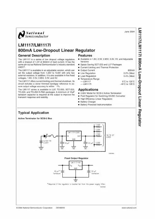
LM1117/LM1117I800mA Low-Dropout Linear RegulatorGeneral DescriptionThe LM1117is a series of low dropout voltage regulators with a dropout of 1.2V at 800mA of load current.It has the same pin-out as National Semiconductor’s industry standard LM317.The LM1117is available in an adjustable version,which can set the output voltage from 1.25V to 13.8V with only two external resistors.In addition,it is also available in five fixed voltages,1.8V,2.5V,2.85V,3.3V,and 5V.The LM1117offers current limiting and thermal shutdown.Its circuit includes a zener trimmed bandgap reference to as-sure output voltage accuracy to within ±1%.The LM1117series is available in LLP ,TO-263,SOT-223,TO-220,and TO-252D-PAK packages.A minimum of 10µF tantalum capacitor is required at the output to improve the transient response and stability.Featuresn Available in 1.8V,2.5V,2.85V,3.3V,5V,and Adjustable Versionsn Space Saving SOT-223and LLP Packages n Current Limiting and Thermal Protection n Output Current 800mA n Line Regulation 0.2%(Max)n Load Regulation 0.4%(Max)n Temperature Range —LM11170˚C to 125˚C —LM1117I −40˚C to 125˚CApplicationsn 2.85V Model for SCSI-2Active Termination n Post Regulator for Switching DC/DC Converter n High Efficiency Linear Regulators n Battery ChargernBattery Powered InstrumentationTypical ApplicationActive Terminator for SCSI-2Bus10091905Fixed Output Regulator10091928June 2004LM1117/LM1117I 800mA Low-Dropout Linear Regulator©2004National Semiconductor Corporation Ordering InformationPackage TemperatureRange Part Number Packaging MarkingTransport Media NSC Drawing 3-lead SOT-2230˚C to +125˚CLM1117MPX-ADJ N03A Tape and Reel MP04ALM1117MPX-1.8N12A Tape and Reel LM1117MPX-2.5N13A Tape and Reel LM1117MPX-2.85N04A Tape and Reel LM1117MPX-3.3N05A Tape and Reel LM1117MPX-5.0N06A Tape and Reel −40˚C to +125˚CLM1117IMPX-ADJ N03B Tape and Reel LM1117IMPX-3.3N05B Tape and Reel LM1117IMPX-5.0N06B Tape and Reel3-lead TO-2200˚C to +125˚CLM1117T-ADJ LM1117T-ADJ Rails T03B LM1117T-1.8LM1117T-1.8Rails LM1117T-2.5LM1117T-2.5Rails LM1117T-2.85LM1117T-2.85Rails LM1117T-3.3LM1117T-3.3Rails LM1117T-5.0LM1117T-5.0Rails 3-lead TO-2520˚C to +125˚CLM1117DTX-ADJ LM1117DT-ADJ Tape and Reel TD03B LM1117DTX-1.8LM1117DT-1.8Tape and Reel LM1117DTX-2.5LM1117DT-2.5Tape and Reel LM1117DTX-2.85LM1117DT-2.85Tape and Reel LM1117DTX-3.3LM1117DT-3.3Tape and Reel LM1117DTX-5.0LM1117DT-5.0Tape and Reel −40˚C to +125˚CLM1117IDTX-ADJ LM1117IDT-ADJ Tape and Reel LM1117IDTX-3.3LM1117IDT-3.3Tape and Reel LM1117IDTX-5.0LM1117IDT-5.0Tape and Reel 8-lead LLP0˚C to +125˚CLM1117LDX-ADJ 1117ADJ Tape and Reel LDC08A LM1117LDX-1.81117-18Tape and Reel LM1117LDX-2.51117-25Tape and Reel LM1117LDX-2.851117-28Tape and Reel LM1117LDX-3.31117-33Tape and Reel LM1117LDX-5.01117-50Tape and Reel −40˚C to 125˚CLM1117ILDX-ADJ 1117IAD Tape and Reel LM1117ILDX-3.31117I33Tape and Reel LM1117ILDX-5.01117I50Tape and Reel TO-2630˚C to +125˚CLM1117SX-ADJ LM1117SADJ Tape and Reel TS3B LM1117SX-2.85LM1117S2.85Tape and Reel LM1117SX-3.3LM1117S3.3Tape and Reel LM1117SX-5.0LM1117S5.0Tape and ReelL M 1117/L M 1117I 2Block Diagram10091901Connection DiagramsSOT-22310091904Top ViewTO-22010091902Top ViewTO-25210091938Top ViewTO-26310091944Top View10091945Side ViewLLP10091946When using the LLP packagePins2,3&4must be connected together andPins5,6&7must be connected togetherTop ViewLM1117/LM1117I3Absolute Maximum Ratings (Note 1)If Military/Aerospace specified devices are required,please contact the National Semiconductor Sales Office/Distributors for availability and specifications.Maximum Input Voltage (V IN to GND)20VPower Dissipation (Note 2)Internally LimitedJunction Temperature (T J )(Note 2)150˚CStorage Temperature Range -65˚C to 150˚CLead TemperatureTO-220(T)Package 260˚C,10sec SOT-223(IMP)Package 260˚C,4secESD Tolerance (Note 3)2000VOperating Ratings (Note 1)Input Voltage (V IN to GND)15VJunction Temperature Range (T J )(Note 2)LM11170˚C to 125˚C LM1117I−40˚C to 125˚CLM1117Electrical CharacteristicsTypicals and limits appearing in normal type apply for T J =25˚C.Limits appearing in Boldface type apply over the entire junc-tion temperature range for operation,0˚C to 125˚C.Symbol Parameter ConditionsMin (Note 5)Typ (Note 4)Max (Note 5)UnitsV REFReference VoltageLM1117-ADJI OUT =10mA,V IN -V OUT =2V,T J =25˚C 10mA ≤I OUT ≤800mA,1.4V ≤V IN -V OUT ≤10V1.2381.2251.2501.2501.2621.270V VV OUTOutput VoltageLM1117-1.8I OUT =10mA,V IN =3.8V,T J =25˚C 0≤I OUT ≤800mA,3.2V ≤V IN ≤10V 1.7821.746 1.8001.800 1.8181.854V V LM1117-2.5I OUT =10mA,V IN =4.5V,T J =25˚C 0≤I OUT ≤800mA,3.9V ≤V IN ≤10V 2.4752.450 2.5002.500 2.5252.550V V LM1117-2.85I OUT =10mA,V IN =4.85V,T J =25˚C 0≤I OUT ≤800mA,4.25V ≤V IN ≤10V 0≤I OUT ≤500mA,V IN =4.10V 2.8202.7902.790 2.8502.8502.850 2.8802.9102.910V V V LM1117-3.3I OUT =10mA,V IN =5V T J =25˚C 0≤I OUT ≤800mA,4.75V ≤V IN ≤10V 3.2673.235 3.3003.300 3.3333.365V V LM1117-5.0I OUT =10mA,V IN =7V,T J =25˚C 0≤I OUT ≤800mA,6.5V ≤V IN ≤12V4.9504.9005.0005.000 5.0505.100V V ∆V OUTLine Regulation (Note 6)LM1117-ADJI OUT =10mA,1.5V ≤V IN -V OUT ≤13.75V 0.0350.2%LM1117-1.8I OUT =0mA,3.2V ≤V IN ≤10V 16mV LM1117-2.5I OUT =0mA,3.9V ≤V IN ≤10V 16mVLM1117-2.85I OUT =0mA,4.25V ≤V IN ≤10V 16mV LM1117-3.3I OUT =0mA,4.75V ≤V IN ≤15V 16mV LM1117-5.0I OUT =0mA,6.5V ≤V IN ≤15V110mVL M 1117/L M 1117I 4LM1117Electrical Characteristics(Continued)Typicals and limits appearing in normal type apply for T J=25˚C.Limits appearing in Boldface type apply over the entire junc-tion temperature range for operation,0˚C to125˚C.Symbol Parameter ConditionsMin(Note5)Typ(Note4)Max(Note5)Units∆V OUT Load Regulation(Note6)LM1117-ADJV IN-V OUT=3V,10≤I OUT≤800mA0.20.4% LM1117-1.8V IN=3.2V,0≤I OUT≤800mA110mVLM1117-2.5V IN=3.9V,0≤I OUT≤800mA110mVLM1117-2.85V IN=4.25V,0≤I OUT≤800mA110mV LM1117-3.3V IN=4.75V,0≤I OUT≤800mA110mV LM1117-5.0V IN=6.5V,0≤I OUT≤800mA115mVV IN-V OUT Dropout Voltage(Note7)I OUT=100mA 1.10 1.20V I OUT=500mA 1.15 1.25V I OUT=800mA 1.20 1.30VI LIMIT Current Limit V IN-V OUT=5V,T J=25˚C80012001500mAMinimum Load Current(Note8)LM1117-ADJV IN=15V 1.75mAQuiescent Current LM1117-1.8V IN≤15V510mALM1117-2.5V IN≤15V510mALM1117-2.85V IN≤10V510mALM1117-3.3V IN≤15V510mALM1117-5.0V IN≤15V510mA Thermal Regulation T A=25˚C,30ms Pulse0.010.1%/W Ripple Regulation f RIPPLE=120Hz,V IN-V OUT=3V V RIPPLE=1V PP6075dB Adjust Pin Current60120µAAdjust Pin Current Change 10≤I OUT≤800mA,1.4V≤V IN-V OUT≤10V0.25µATemperature Stability0.5% Long Term Stability T A=125˚C,1000Hrs0.3% RMS Output Noise(%of V OUT),10Hz≤f≤10kHz0.003%Thermal Resistance Junction-to-Case 3-Lead SOT-22315.0˚C/W 3-Lead TO-220 3.0˚C/W 3-Lead TO-25210˚C/WThermal Resistance Junction-to-Ambient (No air flow)3-Lead SOT-223(No heat sink)136˚C/W3-Lead TO-220(No heat sink)79˚C/W3-Lead TO-252(Note9)(No heat sink)92˚C/W3-Lead TO-26355˚C/W8-Lead LLP(Note10)40˚C/WLM1117/LM1117I5LM1117I Electrical CharacteristicsTypicals and limits appearing in normal type apply for T J =25˚C.Limits appearing in Boldface type apply over the entire junc-tion temperature range for operation,−40˚C to 125˚C.Symbol Parameter ConditionsMin (Note 5)Typ (Note 4)Max (Note 5)UnitsV REFReference VoltageLM1117I-ADJI OUT =10mA,V IN -V OUT =2V,T J =25˚C 10mA ≤I OUT ≤800mA,1.4V ≤V IN -V OUT ≤10V1.2381.2001.2501.2501.2621.290V VV OUTOutput VoltageLM1117I-3.3I OUT =10mA,V IN =5V,T J =25˚C 0≤I OUT ≤800mA,4.75V ≤V IN ≤10V 3.2673.168 3.3003.300 3.3333.432V V LM1117I-5.0I OUT =10mA,V IN =7V,T J =25˚C 0≤I OUT ≤800mA,6.5V ≤V IN ≤12V4.9504.8005.0005.000 5.0505.200V V ∆V OUTLine Regulation (Note 6)LM1117I-ADJI OUT =10mA,1.5V ≤V IN -V OUT ≤13.75V 0.0350.3%LM1117I-3.3I OUT =0mA,4.75V ≤V IN ≤15V 110mV LM1117I-5.0I OUT =0mA,6.5V ≤V IN ≤15V115mV ∆V OUTLoad Regulation (Note 6)LM1117I-ADJV IN -V OUT =3V,10≤I OUT ≤800mA 0.20.5%LM1117I-3.3V IN =4.75V,0≤I OUT ≤800mA 115mV LM1117I-5.0V IN =6.5V,0≤I OUT ≤800mA120mV V IN -V OUTDropout Voltage (Note 7)I OUT =100mA 1.10 1.30V I OUT =500mA 1.15 1.35V I OUT =800mA1.20 1.40V I LIMITCurrent Limit V IN -V OUT =5V,T J =25˚C 80012001500mA Minimum Load Current (Note 8)LM1117I-ADJ V IN =15V 1.75mA Quiescent CurrentLM1117I-3.3V IN ≤15V 515mA LM1117I-5.0V IN ≤15V515mA Thermal Regulation T A =25˚C,30ms Pulse0.010.1%/W Ripple Regulation f RIPPLE =120Hz,V IN -V OUT =3V V RIPPLE =1V PP6075dBAdjust Pin Current 60120µA Adjust Pin Current Change10≤I OUT ≤800mA,1.4V ≤V IN -V OUT ≤10V 0.210µA Temperature Stability 0.5%Long Term Stability T A =125˚C,1000Hrs0.3%RMS Output Noise (%of V OUT ),10Hz ≤f ≤10kHz 0.003%Thermal Resistance Junction-to-Case 3-Lead SOT-22315.0˚C/W 3-Lead TO-25210˚C/W Thermal Resistance Junction-to-Ambient No air flow)3-Lead SOT-223(No heat sink)136˚C/W 3-Lead TO-252(No heat sink)(Note 9)92˚C/W 8-Lead LLP(Note 10)40˚C/WNote 1:Absolute Maximum Ratings indicate limits beyond which damage to the device may occur.Operating Ratings indicate conditions for which the device is intended to be functional,but specific performance is not guaranteed.For guaranteed specifications and the test conditions,see the Electrical Characteristics.L M 1117/L M 1117I 6Note 2:The maximum power dissipation is a function of T J(max),θJA ,and T A .The maximum allowable power dissipation at any ambient temperature is P D =(T J(max)–T A )/θJA .All numbers apply for packages soldered directly into a PC board.Note 3:For testing purposes,ESD was applied using human body model,1.5k Ωin series with 100pF.Note 4:Typical Values represent the most likely parametric norm.Note 5:All limits are guaranteed by testing or statistical analysis.Note 6:Load and line regulation are measured at constant junction room temperature.Note 7:The dropout voltage is the input/output differential at which the circuit ceases to regulate against further reduction in input voltage.It is measured when the output voltage has dropped 100mV from the nominal value obtained at V IN =V OUT +1.5V.Note 8:The minimum output current required to maintain regulation.Note 9:Minimum pad size of 0.038in 2Note 10:Thermal Performance for the LLP was obtained using JESD51-7board with six vias and an ambient temperature of 22˚C.For information about improved thermal performance and power dissipation for the LLP ,refer to Application Note AN-1187.Typical Performance CharacteristicsDropout Voltage (V IN -VOUT )Short-Circuit Current1009192210091923Load Regulation LM1117-ADJ Ripple Rejection1009194310091906LM1117/LM1117I7Typical Performance Characteristics(Continued)LM1117-ADJ Ripple Rejection vs.CurrentTemperature Stability1009190710091925Adjust Pin Current LM1117-2.85Load Transient Response1009192610091908LM1117-5.0Load Transient Response LM1117-2.85Line Transient Response1009190910091910L M 1117/L M 1117I 8Typical Performance Characteristics(Continued) LM1117-5.0Line Transient Response10091911Application Note1.0External Capacitors/Stability1.1Input Bypass CapacitorAn input capacitor is recommended.A10µF tantalum on theinput is a suitable input bypassing for almost all applications.1.2Adjust Terminal Bypass CapacitorThe adjust terminal can be bypassed to ground with a by-pass capacitor(C ADJ)to improve ripple rejection.This by-pass capacitor prevents ripple from being amplified as theoutput voltage is increased.At any ripple frequency,theimpedance of the C ADJ should be less than R1to prevent theripple from being amplified:1/(2π*f RIPPLE*C ADJ)<R1The R1is the resistor between the output and the adjust pin.Its value is normally in the range of100-200Ω.For example,with R1=124Ωand f RIPPLE=120Hz,the C ADJ should be>11µF.1.3Output CapacitorThe output capacitor is critical in maintaining regulator sta-bility,and must meet the required conditions for both mini-mum amount of capacitance and ESR(Equivalent Series Resistance).The minimum output capacitance required by the LM1117is10µF,if a tantalum capacitor is used.Any increase of the output capacitance will merely improve the loop stability and transient response.The ESR of the output capacitor should range between0.3Ω-22Ω.In the case of the adjustable regulator,when the C ADJ is used,a larger output capacitance(22µf tantalum)is required.2.0Output VoltageThe LM1117adjustable version develops a1.25V reference voltage,V REF,between the output and the adjust terminal. As shown in Figure1,this voltage is applied across resistor R1to generate a constant current I1.The current I ADJ from the adjust terminal could introduce error to the output.But since it is very small(60µA)compared with the I1and very constant with line and load changes,the error can be ig-nored.The constant current I1then flows through the output set resistor R2and sets the output voltage to the desired level.For fixed voltage devices,R1and R2are integrated inside the devices.3.0Load RegulationThe LM1117regulates the voltage that appears between itsoutput and ground pins,or between its output and adjustpins.In some cases,line resistances can introduce errors tothe voltage across the load.To obtain the best load regula-tion,a few precautions are needed.Figure2,shows a typical application using a fixed outputregulator.The Rt1and Rt2are the line resistances.It isobvious that the V LOAD is less than the V OUT by the sum ofthe voltage drops along the line resistances.In this case,theload regulation seen at the R LOAD would be degraded fromthe data sheet specification.To improve this,the load shouldbe tied directly to the output terminal on the positive side anddirectly tied to the ground terminal on the negative side.10091917FIGURE1.Basic Adjustable RegulatorLM1117/LM1117I9Application Note(Continued)When the adjustable regulator is used (Figure 3),the best performance is obtained with the positive side of the resistor R1tied directly to the output terminal of the regulator rather than near the load.This eliminates line drops from appearing effectively in series with the reference and degrading regu-lation.For example,a 5V regulator with 0.05Ωresistance between the regulator and load will have a load regulation due to line resistance of 0.05Ωx I L .If R1(=125Ω)is con-nected near the load,the effective line resistance will be 0.05Ω(1+R2/R1)or in this case,it is 4times worse.In addition,the ground side of the resistor R2can be returned near the ground of the load to provide remote ground sens-ing and improve load regulation.4.0Protection DiodesUnder normal operation,the LM1117regulators do not need any protection diode.With the adjustable device,the internal resistance between the adjust and output terminals limits the current.No diode is needed to divert the current around the regulator even with capacitor on the adjust terminal.The adjust pin can take a transient signal of ±25V with respect to the output voltage without damaging the device.When a output capacitor is connected to a regulator and the input is shorted to ground,the output capacitor will discharge into the output of the regulator.The discharge current de-pends on the value of the capacitor,the output voltage of the regulator,and rate of decrease of V IN .In the LM1117regu-lators,the internal diode between the output and input pins can withstand microsecond surge currents of 10A to 20A.With an extremely large output capacitor (≥1000µF),and with input instantaneously shorted to ground,the regulator could be damaged.In this case,an external diode is recommended between the output and input pins to protect the regulator,as shown in Figure 4.5.0Heatsink RequirementsWhen an integrated circuit operates with an appreciable current,its junction temperature is elevated.It is important to quantify its thermal limits in order to achieve acceptable performance and reliability.This limit is determined by sum-ming the individual parts consisting of a series of tempera-ture rises from the semiconductor junction to the operating environment.A one-dimensional steady-state model of con-duction heat transfer is demonstrated in Figure 5.The heat generated at the device junction flows through the die to the die attach pad,through the lead frame to the surrounding case material,to the printed circuit board,and eventually to the ambient environment.Below is a list of variables that may affect the thermal resistance and in turn the need for a heatsink.R θJC (ComponentVariables)R θCA (ApplicationVariables)Leadframe Size &Material Mounting Pad Size,Material,&Location No.of Conduction Pins Placement of Mounting PadDie SizePCB Size &Material Die Attach Material Traces Length &Width Molding Compound Size and MaterialAdjacent Heat Sources Volume of Air Ambient Temperatue Shape of Mounting Pad10091918FIGURE 2.Typical Application using Fixed OutputRegulator 10091919FIGURE 3.Best Load Regulation using AdjustableOutput Regulator 10091915FIGURE 4.Regulator with Protection Diode L M 1117/L M 1117I10Application Note(Continued)The LM1117regulators have internal thermal shutdown to protect the device from over-heating.Under all possible operating conditions,the junction temperature of the LM1117must be within the range of 0˚C to 125˚C.A heatsink may be required depending on the maximum power dissipation and maximum ambient temperature of the application.To deter-mine if a heatsink is needed,the power dissipated by the regulator,P D ,must be calculated:I IN =I L +I GP D =(V IN -V OUT )I L +V IN I GFigure 6shows the voltages and currents which are present in the circuit.The next parameter which must be calculated is the maxi-mum allowable temperature rise,T R (max):T R (max)=T J (max)-T A (max)where T J (max)is the maximum allowable junction tempera-ture (125˚C),and T A (max)is the maximum ambient tem-perature which will be encountered in the application.Using the calculated values for T R (max)and P D ,the maxi-mum allowable value for the junction-to-ambient thermal resistance (θJA )can be calculated:θJA =T R (max)/P DIf the maximum allowable value for θJA is found to be ≥136˚C/W for SOT-223package or ≥79˚C/W for TO-220package or ≥92˚C/W for TO-252package,no heatsink is needed since the package alone will dissipate enough heat to satisfy these requirements.If the calculated value for θJA falls below these limits,a heatsink is required.As a design aid,Table 1shows the value of the θJA of SOT-223and TO-252for different heatsink area.The copper patterns that we used to measure these θJA s are shown at the end of the Application Notes Section.Figure 7and Figure 8reflects the same test results as what are in the Table 1Figure 9and Figure 10shows the maximum allowable power dissipation vs.ambient temperature for the SOT-223and TO-252device.Figures Figure 11and Figure 12shows the maximum allowable power dissipation vs.copper area (in 2)for the SOT-223and TO-252devices.Please see AN1028for power enhancement techniques to be used with SOT-223and TO-252packages.*Application Note AN-1187discusses improved thermal per-formance and power dissipation for the LLP .TABLE 1.θJA Different Heatsink AreaLayout Copper AreaThermal ResistanceTop Side (in 2)*Bottom Side (in 2)(θJA ,˚C/W)SOT-223(θJA ,˚C/W)TO-25210.0123013610320.0660*******.30846040.530755450.76069526106647700.211584800.49870900.689631000.8825711017957120.0660.06612589130.1750.175937210091937FIGURE 5.Cross-sectional view of Integrated Circuit Mounted on a printed circuit board.Note that the case temperature is measured at the point where the leadscontact with the mounting pad surface 10091916FIGURE 6.Power Dissipation DiagramLM1117/LM1117IApplication Note(Continued)TABLE 1.θJA Different Heatsink Area (Continued)Layout Copper AreaThermal Resistance140.2840.2848361150.3920.3927555160.50.57053*Tab of device attached to topside copperL M 1117/L M 1117IApplication Note(Continued)10091913 FIGURE7.θJA vs.1oz Copper Area for SOT-22310091934 FIGURE8.θJA vs.2oz Copper Area for TO-25210091912 FIGURE9.Maximum Allowable Power Dissipation vs.Ambient Temperature for SOT-22310091936FIGURE10.Maximum Allowable Power Dissipation vs.Ambient Temperature for TO-25210091914FIGURE11.Maximum Allowable Power Dissipation vs.1oz Copper Area for SOT-22310091935FIGURE12.Maximum Allowable Power Dissipation vs.2oz Copper Area for TO-252LM1117/LM1117IApplication Note(Continued)10091941FIGURE 13.Top View of the Thermal Test Pattern in Actual ScaleL M 1117/L M 1117IApplication Note(Continued)10091942FIGURE14.Bottom View of the Thermal Test Pattern in Actual Scale LM1117/LM1117ITypical Application Circuits10091930Adjusting Output of Fixed Regulators10091931Regulator with Reference100919291.25V to 10V Adjustable Regulator with ImprovedRipple Rejection100919275V Logic Regulator with Electronic Shutdown*L M 1117/L M 1117ITypical Application Circuits(Continued)10091932Battery Backed-Up Regulated Supply10091933Low Dropout Negative Supply LM1117/LM1117IPhysical Dimensionsinches (millimeters)unless otherwise noted3-Lead SOT-223NS Package Number MP04A3-Lead TO-220NS Package Number T03BL M 1117/L M 1117IPhysical Dimensions inches(millimeters)unless otherwise noted(Continued)3-Lead TO-263NS Package Number TS3B LM1117/LM1117IPhysical Dimensionsinches (millimeters)unless otherwise noted (Continued)3-Lead TO-252NS Package Number TD03B8-Lead LLPNS Package Number LDC08AL M 1117/L M 1117INotesLIFE SUPPORT POLICYNATIONAL’S PRODUCTS ARE NOT AUTHORIZED FOR USE AS CRITICAL COMPONENTS IN LIFE SUPPORT DEVICES OR SYSTEMS WITHOUT THE EXPRESS WRITTEN APPROVAL OF THE PRESIDENT AND GENERAL COUNSEL OF NATIONAL SEMICONDUCTOR CORPORATION.As used herein:1.Life support devices or systems are devices orsystems which,(a)are intended for surgical implant into the body,or(b)support or sustain life,and whose failure to perform when properly used in accordance with instructions for use provided in the labeling,can be reasonably expected to result in a significant injury to the user.2.A critical component is any component of a lifesupport device or system whose failure to perform can be reasonably expected to cause the failure of the life support device or system,or to affect its safety or effectiveness.BANNED SUBSTANCE COMPLIANCENational Semiconductor certifies that the products and packing materials meet the provisions of the Customer Products Stewardship Specification(CSP-9-111C2)and the Banned Substances and Materials of Interest Specification (CSP-9-111S2)and contain no‘‘Banned Substances’’as defined in CSP-9-111S2.National Semiconductor Americas CustomerSupport CenterEmail:new.feedback@ Tel:1-800-272-9959National SemiconductorEurope Customer Support CenterFax:+49(0)180-5308586Email:europe.support@Deutsch Tel:+49(0)6995086208English Tel:+44(0)8702402171Français Tel:+33(0)141918790National SemiconductorAsia Pacific CustomerSupport CenterEmail:ap.support@National SemiconductorJapan Customer Support CenterFax:81-3-5639-7507Email:jpn.feedback@Tel:81-3-5639-7560 LM1117/LM1117I 800mA Low-Dropout Linear RegulatorNational does not assume any responsibility for use of any circuitry described,no circuit patent licenses are implied and National reserves the right at any time without notice to change said circuitry and specifications.。
LM1117是一个低压差电压调节器系列。
其压差在1.2V输出,负载电流为800mA时为1.2V。
它与国家半导体的工业标准器件LM317有相同的管脚排列。
LM1117有可调电压的版本,通过2个外部电阻可实现1.25~13.8V输出电压范围。
另外还有5个固定电压输出(1.8V、2.5V、2.85V、3.3V和5V)的型号。
LM1117提供电流限制和热保护。
电路包含1个齐纳调节的带隙参考电压以确保输出电压的精度在±1%以内。
LM1117系列具有LLP、TO-263、SOT-223、TO-220和TO-252 D-PAK封装。
输出端需要一个至少10uF的钽电容来改善瞬态响应和稳定性。
替换型号X1117是IC网络超市自主的品牌,可以很好的替换LM1117。
X1117是一款正电压输出的低压降三端线性稳压电路,在1A输出电流下的压降为1.2V。
分为两个版本,固定电压输出版本和可调电压输出版本。
固定输出电压1.5V、1.8V、2.5V、3.3V、5.0V和可调版本的电压精度为1%;固定电压为1.2V的产品输出电压精度为2%。
内部集成过热保护和限流电路,适用于各类电子产品。
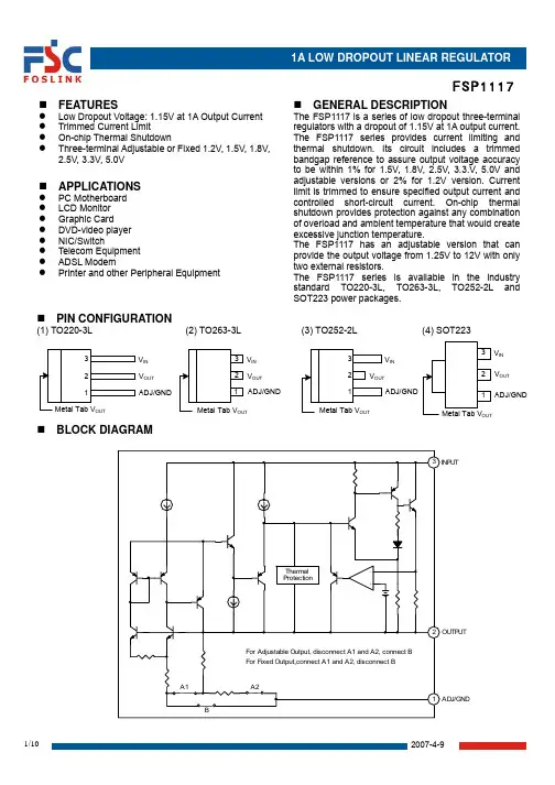
A1117是台湾亿光研发生产的高效率低压降三端线性稳压器,A1117提供电流限制和热保护,以确保芯片和功率稳定性系统。
而在芯片上保证输出电压精度在±2%。
同时也提供了固定电压输出版本和可调电压输出版本,可调版本能输出从1.25V到13.8V。
特性提供1.8V、2.5V、2.85V、3.3V、5V和可调电压的型号节省空间的SOT-223和LLP封装电流限制和热保护功能输出电流可达800mA线性调整率:0.2% (Max)负载调整率:0.4% (Max)温度范围-LM1117:0℃~125℃-LM1117I:-40℃~125℃2.85V模块可用于SCSI-2有源终端开关DC/DC转换器的主调压器高效线性调整器电池充电器电池供电装置典型应用电路图。
N/C V OUT V OUTN/CAdvanced AMS1117Monolithic 1A LOW DROPOUT VOLTAGE REGULATORSystemsRoHs Compli antFEATURESAPPLICATIONS• Three Terminal Adjustable or Fixed Voltages* • High Efficiency Linear Regulators 1.5V, 1.8V, 2.5V, 2.85V, 3.3V and 5.0V • Post Regulators for Switching Supplies • Output Current of 1A• 5V to 3.3V Linear Regulator • Operates Down to 1V Dropout • Battery Chargers• Line Regulation: 0.2% Max. • Active SCSI Terminators• Load Regulation: 0.4% Max.• Power Management for Notebook • SOT-223, TO-252 and SO-8 package available• Battery Powered InstrumentationGENERAL DESCRIPTIONThe AMS1117 series of adjustable and fixed voltage regulators are designed to provide up to1A output current and to operate down to 1V input-to-output differential. The dropout voltage of the device is guaranteed maximum 1.3V, decreasing at lower load currents.On-chip trimming adjusts the reference voltage to 1.5%. Current limit is set to minimize the stress under overload conditions on both the regulator and power source circuitry.The AMS1117 devices are pin compatible with other three-terminal SCSI regulators and are offered in the low profile surface mount SOT-223 package, in the 8L SOIC package and in the TO-252 (DPAK) plastic package.ORDERING INFORMATION:PIN CONNECTIONSSOT-223 Top View8L SOIC Top ViewV OUT V OUT V IN3 PIN FIXED/ADJUSTABLEVERSION1- Ground/Adjust123TAB ISTO-252 FRONT VIEW313- V INABSOLUTE MAXIMUM RATINGS (Note 1)Power Dissipation Internally limited Soldering informationInput Voltage 15V Lead Temperature (25 sec) 265°C Operating Junction Temperature Thermal ResistanceControl Section Power Transistor Storage temperature-40°C to 125°C-40°C to 125°C- 65°C to +150°CSO-8 packageTO-252 packageSOT-223 package* With package so l d e r i ngϕJA= 160°C/WϕJA= 80°C/WϕJA= 90°C/W*to copper area over backsideground plane or internal power plane ϕJA can vary from46°C/W to >90°C/W depending on mounting technique andthe size of the copper area.ELECTRICAL CHARACTERISTICSELECTRICAL CHARACTERISTICSParameters identified with boldface type apply over the full operating temperature range.Note 1: Absolute Maximum Ratings indicate limits beyond which damage to the device may occur. For guaranteed specifications and test conditions, see the Electrical Characteristics. The guaranteed specifications apply only for the test conditions listed.Note 2: Line and Load regulation are guaranteed up to the maximum power dissipation of 1.2 W for SOT-223, 2.2W for TO-252 and 780mW for 8-Lead SOIC. Power dissipation is determined by the input/output differential and the output current. Guaranteed maximum power dissipation will not be available over the full input/output range.Note 3: See thermal regulation specifications for changes in output voltage due to heating effects. Line and load regulation are measured at a constant junction temperature by low duty cycle pulse testing. Load regulation is measured at the output lead ~1/8” from the package.Note 4: Dropout voltage is specified up to 0.8A load. For currents over 0.8A dropout will be higherNote 5: Minimum load current is defined as the minimum output current required to maintain regulation. When 1.5V ≤(V IN - V OUT) ≤12V the device is guaranteed to regulate if the output current is greater than 10mA.APPLICATION HINTSThe AMS1117 series of adjustable and fixed regulators are easy to use and are protected against short circuit and thermal overloads. Thermal protection circuitry will shut-down the regulator should the junction temperature exceed 165°C at the sense point.Pin compatible with older three terminal adjustable regulators, these devices offer the advantage of a lower dropout voltage, more precise reference tolerance and improved reference stability with temperature.V IND1V OUTStabilityThe circuit design used in the AMS1117 series requires the use ofan output capacitor as part of the device frequency compensation. The addition of 22µF solid tantalum on the output will ensure stability for all operating conditions.When the adjustment terminal is bypassed with a capacitor to improve the ripple rejection, the requirement for an output capacitor increases. The value of 22µF tantalum covers all cases of bypassing the adjustment terminal. Without bypassing theOutput VoltageĤigure 1.Fadjustment terminal smaller capacitors can be used with equally good results.To further improve stability and transient response of these devices larger values of output capacitor can be used.Protection DiodesThe AMS1117 series develops a 1.25V reference voltage between the output and the adjust terminal. Placing a resistor between these two terminals causes a constant current to flow through R1 and down through R2 to set the overall output voltage. This current is normally the specified minimum load current of 10mA. Because I ADJ is very small and constant it represents a small error and it can usually be ignored.Unlike older regulators, the AMS1117 family does not need any protection diodes between the adjustment pin and the output and from the output to the input to prevent over-stressing the die. Internal resistors are limiting the internal current paths on the AMS1117 adjustment pin, therefore even with capacitors on the adjustment pin no protection diode is needed to ensure device safety under short-circuit conditions.Diodes between the input and output are not usually needed.VV OUT Microsecond surge currents of 50A to 100A can be handled by the internal diode between the input and output pins of the device. In normal operations it is difficult to get those values of surge currents even with the use of large output capacitances. If high value output capacitors are used, such as 1000µF to 5000µF and the input pin is instantaneously shorted to ground, damage can occur. A diode from output to input is recommended, when a crowbar circuit at the input of the AMS1117 is used (Figure 1).V OUT = V REF ADJ R2Figure 2. Basic Adjustable R e gu l ato rLoad RegulationTrue remote load sensing it is not possible to provide, because the AMS1117 is a three terminal device. The resistance of the wire connecting the regulator to the load will limit the load regulation. The data sheet specification for load regulation is measured at the bottom of the package. Negative side sensing is a true Kelvin connection, with the bottom of the output divider returned to the negative side of the load.The best load regulation is obtained when the top of the resistor divider R1 is connected directly to the case not to the load. If R1 were connected to the load, the effective resistance between the regulator and the load would be:R P x ( R2+R1 ) ,R P = Parasitic Line ResistanceR1APPLICATION HINTSConnected as shown , R P is not multiplied by the divider ratioR PPARASITIC The total thermal resistance from junction to ambient can be as low as 45°C /W. This requires a reasonable sized PC board with at least on layer of copper to spread the heat across the board and couple it into the surrounding air.V R LExperiments have shown that the heat spreading copper layer does not need to be electrically connected to the tab of the device. The PC material can be very effective at transmitting heat between the pad area, attached to the pad of the device, and a ground plane layer either inside or on the opposite side of the board. Although the actual thermal resistance of the PC material is high, the Length/Area ratio of the thermal resistance between layers is small. The data in Table 1, was taken using 1/16” FR-4 board with 1 oz. copper foil, and it can be used as a rough guideline for estimating thermal resistance.For each application the thermal resistance will be affected by thermal interactions with other components on the board. To determine the actual value some experimentation will be necessary.The power dissipation of the AMS1117 is equal to: *CONNECT R1 TO CASECONNECT R2 TO LOADFigure 3. Connections for Best Load RegulationIn the case of fixed voltage devices the top of R1 is connected Kelvin internally, and the ground pin can be used for negative side sensing.Thermal ConsiderationsThe AMS1117 series have internal power and thermal limiting circuitry designed to protect the device under overload conditions. However maximum junction temperature ratings of 125°C should not be exceeded under continuous normal load conditions.Careful consideration must be given to all sources of thermal resistance from junction to ambient. For the surface mount package SOT-223 additional heat sources mounted near the device must be considered. The heat dissipation capability of the PC board and its copper traces is used as a heat sink for the device. The thermal resistance from the junction to the tab for the AMS1117 is 15°C/W. Thermal resistance from tab to ambient can be as low as 30°C /W.P D = ( V IN - V OUT )( I OUT )Maximum junction temperature will be equal to:T J = T A(MAX) + P D (Thermal Resistance (junction-to-ambient)) Maximum junction temperature must not exceed 125°C.Ripple RejectionThe ripple rejection values are measured with the adjustment pinbypassed. The impedance of the adjust pin capacitor at the ripple frequency should be less than the value of R1 (normally 100Ω to 200Ω) for a proper bypassing and ripple rejection approaching the values shown. The size of the required adjust pin capacitor is a function of the input ripple frequency. If R1=100Ω at 120Hz the adjust pin capacitor should be >13µF. At 10kHz only 0.16µF is needed.The ripple rejection will be a function of output voltage, in circuits without an adjust pin bypass capacitor. The output ripple will increase directly as a ratio of the output voltage to the reference voltage (V OUT / V REF ).O U T P U T V O L T A G E D E V I A T I O N (%)O U T P U T V O L T A G E C H A N G E (%)M I N I M U M O P E R A T I N G C U R R E N T (m A )A D J U S T P I N C U R R E N T (µA )R I P P L E R E J E C T I O N (d B )S H O R T C I R C U I T C U R R E N T (A )10TYPICAL PERFORMANCE CHARACTERISTICSMinimum Operating Current (Adjustable Device)Short-Circuit Current121.2591.0060.750.5030.250 05101520INPUT/OUTPUT DIFFERENTIAL (V) 00 5 10 15INPUT/OUTPUT DIFFERENTIAL0.10Load RegulationRipple Rejection vs. Current1000.05-0.05908070605040 -0.1030-0.1520-0.20-50-25255075100125TEMPERATURE (°C)0.25 0.5 0.75 1.0OUTPUT CURRENT (A)2.0 Temperature Stability100 Adjust Pin Current9080 1.0706050 4030 -1.02010-2.0-50 -25255075100 125 150TEMPERATURE (°C)-50 -25255075100 125 150TEMPERATURE (°C)PACKAGE DIMENSIONS inches (millimeters) unless otherwise noted.TO-252 PLASTIC PACKAGE (D)3 LEAD SOT-223 PLASTIC PACKAGEAMS1117PACKAGE DIMENSIONS inches (millimeters) unless otherwise noted (Continued).8 LEAD SOIC PLASTIC PACKAGE (S)*DIMENSION DOES NOT INCLUDE MOLD FLASH. MOLD FLASH SHALL NOT EXCEED 0.006" (0.152mm) PER SIDE**DIMENSION DOES NOT INCLUDE INTERLEAD FLASH. INTERLEAD FLASH SHALL NOT EXCEED 0.010" (0.254mm) PER SIDE。
am1117的5v转3.3v工作原理
AM1117的5v转3.3v工作原理如下:
AM1117是一款正向低压降稳压器,在1A输出电流下的压降为1.2V。
其工作原理类似于LM317等线性稳压器,通过对输出电压进行采样,并将采样结果反馈到调节电路来调节输出级调整管的阻抗。
当输出电压偏低时,调节输出级的阻抗会变小,从而减小调整管的压降;当输出电压偏高时,调节输出级的阻抗会变大,从而增大调整管的压降。
这样,就能维持输出电压的稳定。
AM1117与78系列稳压器的主要差别在于其最小饱和压降(即失稳电压)较小,典型值为1.1V,最大值为1.3V,而78系列稳压器的失稳电压为2V~3V左右。
因此,在相同的输出电压情况下,AM1117可以在更低的输入工作电压下工作。
此外,以SSM1117-3.3为例,其最低工作电压为4.4V(典型值)~4.8V (最大值),而LM317输出3.3V电压时要求最低输入电压为5.3~6.3V。
在实际应用中,AM1117的输出电流可达1A,且具有出色的线路和负载调整能力。
如果需要更高的输出电流或更低的输出电压,可以通过外接扩流电路来实现。
同时,AM1117还具有过热保护和短路保护功能,可以有效地保护电路和芯片免受损坏。
因此,AM1117的5v转3.3v电路是一种高效、可靠的稳压电路解决方案,适用于各种需要稳定输出电压的电子设备中。
AMS1117-3.3LDO医疗设备电源芯⽚
AMS1117-3.3是⼀种输出电压为3.3V的正向低压降稳压器,适⽤于⾼效率线性稳压器发表开关电源稳压器电池充电器活跃的⼩型计算机系统接⼝终端笔记本电脑的电源管理电池供电的仪器。
AMS1117系列稳压器有可调版与多种固定电压版,设计⽤于提供1A输出电流且⼯作压差可低⾄1V。
在最⼤输出电流时,AMS1117器件的压差保证最⼤不超过1.3V,并随负载电流的减⼩⽽逐渐降低;
AMS1117的⽚上微调把基准电压调整到1.5%的误差以内,⽽且电流限制也得到了调整,以尽量减少因稳压器和电源电路超载⽽造成的压⼒
电⽓特性:
输出电压:3.267~3.333V(0<= IOUT<=1A , 4.75V<=VIN<=12V)线路调整(最⼤):10mV(4.75V<=VIN<=12V)负载调节(最⼤):15mV(VIN=5V,0<= IOUT <=1A)电压差(最⼤):1.3V电流限制:900~1500mA静态电流(最⼤):10mA纹波抑制(最⼩):60dB
技术⽀持:136********:2355239042。
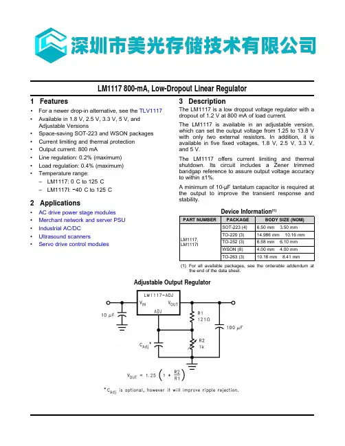
1Features•For a newer drop-in alternative,see the TLV1117•Available in 1.8V,2.5V,3.3V,5V,and Adjustable Versions•Space-saving SOT-223and WSON packages •Current limiting and thermal protection •Output current:800mA•Line regulation:0.2%(maximum)•Load regulation:0.4%(maximum)•Temperature range:–LM1117:0°C to 125°C –LM1117I:−40°C to 125°C2Applications•AC drive power stage modules •Merchant network and server PSU •Industrial AC/DC •Ultrasound scanners•Servo drive control modules3DescriptionThe LM1117is a low dropout voltage regulator with a dropout of 1.2V at 800mA of load current.The LM1117is available in an adjustable version,which can set the output voltage from 1.25to 13.8V with only two external resistors.In addition,it is available in five fixed voltages,1.8V,2.5V,3.3V,and 5V.The LM1117offers current limiting and thermal shutdown.Its circuit includes a Zener trimmed bandgap reference to assure output voltage accuracy to within ±1%.A minimum of 10-µF tantalum capacitor is required at the output to improve the transient response and stability.Device Information (1)PART NUMBERPACKAGE BODY SIZE (NOM)LM1117,LM1117ISOT-223(4) 6.50mm ×3.50mm TO-220(3)14.986mm ×10.16mm TO-252(3) 6.58mm ×6.10mm WSON (8) 4.00mm ×4.00mm TO-263(3)10.18mm ×8.41mm(1)For all available packages,see the orderable addendum atthe end of the data sheet.Adjustable OutputRegulator找Memory 、FPGA 、二三极管、连接器、模块、光耦、电容电阻、单片机、处理器、晶振、传感器、 滤波器,上深圳市美光存储技术有限公司The case temperature is measured at the point where the leads contact with the mounting pad surfaceFigure22.Cross-Sectional View of Integrated Circuit Mounted on a Printed Circuit BoardLM1117SNOS412O –FEBRUARY 2000–REVISED JUNE 2020(1)Tab of device attached to topside copperThe LM1117regulators have internal thermal shutdown to protect the device from over-heating.Under all possible operating conditions,the junction temperature of the LM1117must be within the range of 0°C to 125°C.A heatsink may be required depending on the maximum power dissipation and maximum ambient temperature of the application.To determine if a heatsink is needed,the power dissipated by the regulator,P D ,must be calculated:I IN =I L +I G(2)P D =(V IN -V OUT )I L +V IN I G(3)Figure 23shows the voltages and currents which are present in thecircuit.TAPE AND REELINFORMATION*All dimensions arenominalDevicePackage Type Package Drawing Pins SPQReel Diameter (mm)Reel Width W1(mm)A0(mm)B0(mm)K0(mm)P1(mm)W (mm)Pin1Quadrant LM1117DTX-1.8/NOPB TO-252NDP 32500330.016.4 6.910.5 2.78.016.0Q2LM1117DTX-2.5/NOPB TO-252NDP 32500330.016.4 6.910.5 2.78.016.0Q2LM1117DTX-3.3/NOPB TO-252NDP 32500330.016.4 6.910.5 2.78.016.0Q2LM1117DTX-5.0/NOPB TO-252NDP 32500330.016.4 6.910.5 2.78.016.0Q2LM1117DTX-ADJ/NOPB TO-252NDP 32500330.016.4 6.910.5 2.78.016.0Q2LM1117IDTX-3.3/NOPB TO-252NDP 32500330.016.4 6.910.5 2.78.016.0Q2LM1117IDTX-5.0/NOPB TO-252NDP 32500330.016.4 6.910.5 2.78.016.0Q2LM1117IDTX-ADJ/NOPB TO-252NDP 32500330.016.4 6.910.5 2.78.016.0Q2LM1117ILD-ADJ/NOPB WSON NGN 81000178.012.4 4.3 4.3 1.38.012.0Q1LM1117IMP-3.3/NOPB SOT-223DCY 41000330.016.47.07.5 2.212.016.0Q3LM1117IMP-5.0/NOPBSOT-223DCY 41000330.016.47.07.5 2.212.016.0Q3LM1117IMP-ADJ/NOPB SOT-223DCY 41000330.016.47.07.5 2.212.016.0Q3LM1117IMPX-3.3/NOPB SOT-223DCY 42000330.016.47.07.5 2.212.016.0Q3LM1117IMPX-5.0/NOPB SOT-223DCY 42000330.016.47.07.5 2.212.016.0Q3LM1117IMPX-ADJ/NOPB SOT-223DCY 42000330.016.47.07.5 2.212.016.0Q3LM1117LD-1.8/NOPB WSON NGN 81000178.012.4 4.3 4.3 1.38.012.0Q1LM1117LD-2.5/NOPB WSON NGN 81000178.012.4 4.3 4.3 1.38.012.0Q1LM1117LD-3.3/NOPBWSONNGN81000178.012.44.34.31.38.012.0Q1PACKAGE MATERIALS INFORMATION12-May-2020。
1A Low Dropout Positive Voltage RegulatorLM1117L3Features Description●Adjustable or Fixed Output The LM1117 series of positive adjustable and fixed ●Output Current of 1A regulators are designed to provide 1A with high ●Low Dropout, 1.3V max at 1A Output Current efficiency. All internal circuitry is designed to ●0.04% Line Regulation operate down to 1.3V input to output differential. ●0.2% Load Regulation On-chip trimming adjusts the reference voltage to ●100% Thermal Limit Burn-in 1%.●Fast Transient ResponseApplications●High Efficiency Linear Regulators● Post Regulators for Switching Supplies● Adjustable Power SupplyTypical Application DataFixed V oltage RegulatorAdjustable V oltage RegulatorV OUT =V REF ×(1+R2/R1)+I ADJ ×R21) C1 needed if device is far from filter capacitors2) C2 minimum value required for stabilityC2 10μF Tant.MinV OUT =3.3V C110μF Tant V IN >4.75V 1 23IN TAB GND OUT +V OUT =3.45V C2 10μF Tant.Min R2 232 Ohm,1%C1 10μF, Tant V IN >4.75V + IN TAB ADJ OUT+Package InformationSOT-223Absolute Maximum RatingsSymbol ParameterMaximum Units PD Power DissipationInternally Limited W VIN Input Voltage7 V TJ Operating Junction Temperature RangeControl SectionPower Transistor0 to 125 0 to 150 ℃ TSTG Storage Temperature-65 to 150 ℃ TLEAD Lead Temperature(Soldering, 10 sec) 300 ℃Device Selection GuideDeviceOutput Voltage LM1117-AdjAdjustable LM1117-1.51.5V LM1117-1.81.8V LM1117-2.52.5V LM1117-2.852.8 5V LM1117-3.03. 0V LM1117-3.33.3V LM1117-3.53.5V LM1117-5.05.0VElectrical Characteristics @I LOAD =0mA,T J =25℃, unless otherwise specifiedParameter DeviceTest Conditions Min Typ Max Units V IN =5V,I LOAD =10mA 1.238 1.250 1.262Reference voltage(Note 1) Adj VersionV IN =2.65V to 7V,I LOAD =10mA to 1A * 1.225 1.250 1.275V V IN =V OUT +1.5VVariator from nominal V OUT-1 +1 % V IN =V OUT +1.5V to 7VI LOAD =0mA to 1AOutput Voltage (Note 1) Al fixedversion Variator from nominal V OUT * -2 +2 %Line Regulation (Note 1) All I LOAD =10mA,(V OUT +1.5V)≦V ≦7V * 0.040.2Load Regualtion (Note 1) All V IN =V OUT +1.5V, I LOAD =10mA to 1A * 0.2 0.4%Minimum Load Current Adj Version V IN =5V,V ADJ =0V * 3 7mAGround Pin Current All fixed version V IN =V OUT +1.5V,I LOAD =10mA to 1A *713mAAdjust Pin CurrentAdj Version V IN =2.65V to 7V, I LOAD =10mA * 55 90µA Pin Function1 ADJ/GND2 OUTPUT3 INPUT 1 2 3Current Limit All (V IN -V OUT )=1.5V* 1 A Ripple Rejection (Note 2)All V IN =V OUT +1.5V,I LOAD =1A6072dB Dropout Voltage (Note 1,3)All V IN ≧2.65V, I LOAD = 1A* 1.15 1.3V Temperature CoefficientAll V IN =V OUT=1.5V, I LOAD = 10mA * 0.005 %/℃The * denotes the specifications which apply over the full temperature range.Note 1:Low duty pulse testing with Kelvin connections required.Note 2:120Hz input ripple(CADJ for ADJ=25μF)Note 3:△VOUT, △VREF=1%.Representative Circuit DiagramGND V INV OUT FOR FIXEDVOLTAGEDEVICEFORADJUSTABLEVOLTAGEDEVICE ADJ*: TypicalInches Millimeters Inches Millimeters DIM Min. Max. Min. Max. DIM Min. Max. Min. Max.A 0.1142 0.1220 2.90 3.10 G 0.0551 0.0709 1.40 1.80B 0.2638 0.2874 6.70 7.30 H 0.0098 0.0138 0.25 0.35C 0.1299 0.1457 3.30 3.70 I 0.0008 0.0039 0.02 0.10D 0.0236 0.0315 0.60 0.80 a1 *13o - *13o -E *0.0906 - *2.30 - a2 0 o 10 o 0 o 10 oF 0.2480 0.2638 6.30 6.70Notes: 1.Controlling dimension: millimeters.2.Maximum lead thickness includes lead finish thickness, and minimum lead thickness is the minimum thickness of base material.3.If there is any question with packing specification or packing method, please contact your local CYStek sales office. Material:• Lead: 42 Alloy; solder plating• Mold Compound: Epoxy resin family, flammability solid burning class: UL94V-0Important Notice:• All rights are reserved. Reproduction in whole or in part is prohibited without the prior written approval of CYStek.• CYStek reserves the right to make changes to its products without notice.• CYStek semiconductor products are not warranted to be suitable for use in Life-Support Applications, or systems.• CYStek assumes no liability for any consequence of customer product design, infringement of patents, or application assistance.321FB AC D EG H a1a2I Style: Pin 1.Adj/Gnd 2.Output3.Input3-Lead SOT-223 Plastic Surface Mounted PackageCYStek Package Code: L3左一: 西元年末碼左二: 月碼, 1=A,2=B,…8=H,9=J, …,12=M左三-四: 流水號 Date CodePart number:XX: 15 for 1.5V18 for 1.8V25 for 2.5V33 for 3.3V50 for 5.0VBlank for ADJ。