68013从EEPROM装载固件
- 格式:pdf
- 大小:105.42 KB
- 文档页数:2

CYPRESS 68013A(FX2LP系列)开发手记——驱动程序(2011-01-21 14:36:44)转载一、Cypress USB驱动程序的几个版本截至目前,CY网站上至少公布了三个版本的驱动程序,最后那个SuiteUSB也在更新,罗列几个如下:1,早期EZUSB.SYS,这是给AN2131年代写的驱动程序,90年代公布,目前CY网站上已经删除。
2,后期CYUSB.SYS,这是给FX2和FX2LP写的驱动,是前者的升级版本。
随着《CY3684 EZ-USB FX2LP开发套件》一起发布。
3,2009年开始的SuiteUSB 3.4.2,2011年的3.4.4,同时上述2项废止。
全称叫“SuiteUSB 3.4 - USB Development tools for Visual Studio”,最新3.4.4公布时间2011年01月12日。
2和3可以统称为CYUSB,它和EZUSB的区别如下:1,EZUSB的VID ,PID是04B4,1002,具体由ezusbw2k.inf指定。
这就是所谓通用驱动GPD( General Purpose Drive),主机控制台叫EZ-USB Control Panel。
主机采用WindowsAPI 进行开发,使用标准IOCTL函数。
它由安装CypressEZ-USBDevelopmentKit开发包得到,版本号是261700。
2,CYUSB的VID,PID是04B4,1004,具体由INF文件指定,对应的驱动应该是cyusb.sys,cyusbpre.inf,控制台使用Cypress USB Console。
主机使用CyAPI函数,当然IOCTL也可用(但与老版本有变化,见CYUSB.PDF)。
它由安装“CY3684 EZ-USB FX2LP 开发套件”获得。
最近一次更新时间是2010 年 01 月 05 日,它的软件资料也指向了SuiteUSB,即下面第三条所列。

EZ-USB FX2LP™ USB MicrocontrollerCY7C68013A/CY7C68014A CY7C68015A/CY7C68016A1.0Features (CY7C68013A/14A/15A/16A)•USB 2.0–USB-IF high speed certified (TID # 40440111)•Single-chip integrated USB 2.0 transceiver, smart SIE, and enhanced 8051 microprocessor•Fit, form and function compatible with the FX2—Pin-compatible—Object-code-compatible—Functionally-compatible (FX2LP is a superset)•Ultra Low power: I CC no more than 85 mA in any mode —Ideal for bus and battery powered applications •Software: 8051 code runs from:—Internal RAM, which is downloaded via USB —Internal RAM, which is loaded from EEPROM —External memory device (128 pin package)•16 KBytes of on-chip Code/Data RAM•Four programmable BULK/INTERRUPT/ISOCHRO-NOUS endpoints—Buffering options: double, triple, and quad•Additional programmable (BULK/INTERRUPT) 64-byte endpoint•8- or 16-bit external data interface •Smart Media Standard ECC generation •GPIF (General Programmable Interface)—Allows direct connection to most parallel interface—Programmable waveform descriptors and configu-ration registers to define waveforms—Supports multiple Ready (RDY) inputs and Control (CTL) outputs•Integrated, industry-standard enhanced 8051—48-MHz, 24-MHz, or 12-MHz CPU operation —Four clocks per instruction cycle —Two USARTS—Three counter/timers—Expanded interrupt system —Two data pointers•3.3V operation with 5V tolerant inputs•Vectored USB interrupts and GPIF/FIFO interrupts •Separate data buffers for the Set-up and Data portions of a CONTROL transfer•Integrated I 2C controller, runs at 100 or 400 kHz •Four integrated FIFOs—Integrated glue logic and FIFOs lower system cost —Automatic conversion to and from 16-bit buses —Master or slave operation—Uses external clock or asynchronous strobes —Easy interface to ASIC and DSP ICs•Available in Commercial and Industrial temperature grade (all packages except VFBGA)A d d r e s s (16)x20PLL/0.5/1.0/2.08051 Core 12/24/48 MHz,four clocks/cycleI 2CVCC1.5kD+D–A d d r e s s (16) / D a t aB u s (8)FX2LPGPIFCY Smart USB 1.1/2.0EngineUSB 2.0XCVR16 KB RAM4 kB FIFOIntegrated full- and high-speedXCVRAdditional I/Os (24)ADDR (9)CTL (6)RDY (6)8/16D a t a (8)24 MHz Ext. XTALEnhanced USB core Simplifies 8051 code “Soft Configuration”Easy firmware changes FIFO and endpoint memory (master or slave operation)Up to 96 MBytes/s burst rateGeneralprogrammable I/F to ASIC/DSP or bus standards such as ATAPI, EPP , etc.Abundant I/Oincluding two USARTS High-performance micro using standard toolswith lower-power optionsMasterFigure 1-1. Block Diagramconnected for full speedECC1.1Features (CY7C68013A/14A only)•CY7C68014A: Ideal for battery powered applications —Suspend current: 100 µA (typ)•CY7C68013A: Ideal for non-battery powered applica-tions—Suspend current: 300 µA (typ)•Available in five lead-free packages with up to 40 GPIOs —128-pin TQFP (40 GPIOs), 100-pin TQFP (40 GPIOs),56-pin QFN (24 GPIOs), 56-pin SSOP (24 GPIOs), and 56-pin VFBGA (24 GPIOs)1.2Features (CY7C68015A/16A only)•CY7C68016A: Ideal for battery powered applications—Suspend current: 100 µA (typ)•CY7C68015A: Ideal for non-battery powered applica-tions—Suspend current: 300 µA (typ)•Available in lead-free 56-pin QFN package (26 GPIOs)—2 more GPIOs than CY7C68013A/14A enabling addi-tional features in same footprintCypress Semiconductor Corporation’s (Cypress’s) EZ-USB FX2LP™ (CY7C68013A/14A) is a low-power version of the EZ-USB FX2™ (CY7C68013), which is a highly integrated, low-power USB 2.0 microcontroller. By integrating the USB 2.0 transceiver, serial interface engine (SIE), enhanced 8051 microcontroller, and a programmable peripheral interface in a single chip, Cypress has created a very cost-effective solution that provides superior time-to-market advantages with low power to enable bus powered applications.The ingenious architecture of FX2LP results in data transfer rates of over 53 Mbytes per second, the maximum-allowable USB 2.0 bandwidth, while still using a low-cost 8051 microcon-troller in a package as small as a 56 VFBGA (5mm x 5mm). Because it incorporates the USB 2.0 transceiver, the FX2LP is more economical, providing a smaller footprint solution than USB 2.0 SIE or external transceiver implementations. With EZ-USB FX2LP, the Cypress Smart SIE handles most of the USB 1.1 and 2.0 protocol in hardware, freeing the embedded microcontroller for application-specific functions and decreasing development time to ensure USB compatibility. The General Programmable Interface (GPIF) and Master/Slave Endpoint FIFO (8- or 16-bit data bus) provides an easy and glueless interface to popular interfaces such as ATA, UTOPIA, EPP, PCMCIA, and most DSP/processors. The FX2LP draws considerably less current than the FX2 (CY7C68013), has double the on-chip code/data RAM and is fit, form and function compatible with the 56-, 100-, and 128-pin FX2.Five packages are defined for the family: 56VFBGA, 56 SSOP, 56 QFN, 100 TQFP, and 128 TQFP.2.0 Applications•Portable video recorder•MPEG/TV conversion•DSL modems•ATA interface•Memory card readers•Legacy conversion devices•Cameras•Scanners•Home PNA•Wireless LAN•MP3 players•NetworkingThe “Reference Designs” section of the Cypress web site provides additional tools for typical USB 2.0 applications. Each reference design comes complete with firmware source and object code, schematics, and documentation. Please visit for more information.3.0Functional Overview3.1USB Signaling SpeedFX2LP operates at two of the three rates defined in the USB Specification Revision 2.0, dated April 27, 2000:•Full speed, with a signaling bit rate of 12 Mbps •High speed, with a signaling bit rate of 480 Mbps.FX2LP does not support the low-speed signaling mode of 1.5Mbps.3.28051 MicroprocessorThe 8051 microprocessor embedded in the FX2LP family has 256 bytes of register RAM, an expanded interrupt system,three timer/counters, and two USARTs.3.2.18051 Clock FrequencyFX2LP has an on-chip oscillator circuit that uses an external 24-MHz (±100-ppm) crystal with the following characteristics:•Parallel resonant •Fundamental mode •500-µW drive level•12-pF (5% tolerance) load capacitors.An on-chip PLL multiplies the 24-MHz oscillator up to 480MHz, as required by the transceiver/PHY , and internal counters divide it down for use as the 8051 clock. The default 8051 clock frequency is 12 MHz. The clock frequency of the 8051 can be changed by the 8051 through the CPUCS register, dynamically.The CLKOUT pin, which can be three-stated and inverted using internal control bits, outputs the 50% duty cycle 8051clock, at the selected 8051 clock frequency—48, 24, or 12MHz.3.2.2USARTSFX2LP contains two standard 8051 USARTs, addressed via Special Function Register (SFR) bits. The USART interface pins are available on separate I/O pins, and are not multi-plexed with port pins.UART0 and UART1 can operate using an internal clock at 230KBaud with no more than 1% baud rate error. 230-KBaud operation is achieved by an internally derived clock source that generates overflow pulses at the appropriate time. The internal clock adjusts for the 8051 clock rate (48, 24, 12 MHz)such that it always presents the correct frequency for 230-KBaud operation.[1]3.2.3Special Function RegistersCertain 8051 SFR addresses are populated to provide fast access to critical FX2LP functions. These SFR additions are shown in Table 3-1. Bold type indicates non-standard,enhanced 8051 registers. The two SFR rows that end with “0”and “8” contain bit-addressable registers. The four I/O ports A–D use the SFR addresses used in the standard 8051 for ports 0–3, which are not implemented in FX2LP . Because of the faster and more efficient SFR addressing, the FX2LP I/O ports are not addressable in external RAM space (using the MOVX instruction).3.3I 2C BusFX2LP supports the I 2C bus as a master only at 100-/400-KHz.SCL and SDA pins have open-drain outputs and hysteresis inputs. These signals must be pulled up to 3.3V, even if no I 2C device is connected.3.4BusesAll packages: 8- or 16-bit “FIFO” bidirectional data bus, multi-plexed on I/O ports B and D. 128-pin package: adds 16-bit output-only 8051 address bus, 8-bit bidirectional data bus.Figure 3-1. Crystal Configuration12 pf12 pf24 MHz20 × PLLC1C212-pF capacitor values assumes a trace capacitanceof 3 pF per side on a four-layer FR4 PCANote:1.115-KBaud operation is also possible by programming the 8051 SMOD0 or SMOD1 bits to a “1” for UART0 and/or UART1, respectively.3.5USB Boot MethodsDuring the power-up sequence, internal logic checks the I2C port for the connection of an EEPROM whose first byte is either 0xC0 or 0xC2. If found, it uses the VID/PID/DID values in the EEPROM in place of the internally stored values (0xC0), or it boot-loads the EEPROM contents into internal RAM (0xC2). If no EEPROM is detected, FX2LP enumerates using internally stored descriptors. The default ID values for FX2LP are VID/PID/DID (0x04B4, 0x8613, 0xAxxx where xxx = Chip revision).[2]3.6ReNumeration™Because the FX2LP’s configuration is soft, one chip can take on the identities of multiple distinct USB devices.When first plugged into USB, the FX2LP enumerates automat-ically and downloads firmware and USB descriptor tables over the USB cable. Next, the FX2LP enumerates again, this time as a device defined by the downloaded information. This patented two-step process, called ReNumeration™, happens instantly when the device is plugged in, with no hint that the initial download step has occurred.Two control bits in the USBCS (USB Control and Status) register control the ReNumeration process: DISCON and RENUM. To simulate a USB disconnect, the firmware sets DISCON to 1. To reconnect, the firmware clears DISCON to 0. Before reconnecting, the firmware sets or clears the RENUM bit to indicate whether the firmware or the Default USB Device will handle device requests over endpoint zero: if RENUM = 0, the Default USB Device will handle device requests; if RENUM = 1, the firmware will.3.7Bus-powered ApplicationsThe FX2LP fully supports bus-powered designs by enumer-ating with less than 100 mA as required by the USB 2.0 speci-fication.3.8Interrupt System3.8.1INT2 Interrupt Request and Enable RegistersFX2LP implements an autovector feature for INT2 and INT4. There are 27 INT2 (USB) vectors, and 14 INT4 (FIFO/GPIF) vectors. See EZ-USB Technical Reference Manual (TRM) for more details.3.8.2USB-Interrupt AutovectorsThe main USB interrupt is shared by 27 interrupt sources. To save the code and processing time that normally would be required to identify the individual USB interrupt source, the FX2LP provides a second level of interrupt vectoring, called Autovectoring. When a USB interrupt is asserted, the FX2LP pushes the program counter onto its stack then jumps to address 0x0043, where it expects to find a “jump” instruction to the USB Interrupt service routine.Table 3-1. Special Function Registersx8x9x Ax Bx Cx Dx Ex Fx 0IOA IOB IOC IOD SCON1PSW ACC B 1SP EXIF INT2CLR IOE SBUF12DPL0MPAGE INT4CLR OEA3DPH0OEB4DPL1OEC5DPH1OED6DPS OEE7PCON8TCON SCON0IE IP T2CON EICON EIE EIP 9TMOD SBUF0A TL0AUTOPTRH1EP2468STAT EP01STAT RCAP2LB TL1AUTOPTRL1EP24FIFOFLGS GPIFTRIG RCAP2HC TH0reserved EP68FIFOFLGS TL2D TH1AUTOPTRH2GPIFSGLDATH TH2E CKCON AUTOPTRL2GPIFSGLDATLXF reserved AUTOPTRSET-UP GPIFSGLDATLNOXTable 3-2. Default ID Values for FX2LPDefault VID/PID/DIDVendor ID0x04B4Cypress SemiconductorProduct ID0x8613EZ-USB FX2LPDevice release0xAnnn Depends on chip revision(nnn = chip revision where firstsilicon = 001)Note:2.The I2C bus SCL and SDA pins must be pulled up, even if an EEPROM is not connected. Otherwise this detection method does not work properly.The FX2LP jump instruction is encoded as follows.If Autovectoring is enabled (AV2EN = 1 in the INTSET-UP register), the FX2LP substitutes its INT2VEC byte. Therefore, if the high byte (“page”) of a jump-table address is preloaded at location 0x0044, the automatically-inserted INT2VEC byte at 0x0045 will direct the jump to the correct address out of the 27 addresses within the page.3.8.3FIFO/GPIF Interrupt (INT4)Just as the USB Interrupt is shared among 27 individual USB-interrupt sources, the FIFO/GPIF interrupt is shared among 14 individual FIFO/GPIF sources. The FIFO/GPIF Interrupt, like the USB Interrupt, can employ autovectoring. Table3-4 shows the priority and INT4VEC values for the 14 FIFO/GPIF interrupt sources.Table 3-3. INT2 USB InterruptsUSB INTERRUPT TABLE FOR INT2 Priority INT2VEC Value Source Notes1 00SUDAV Set-up Data Available2 04 SOF Start of Frame (or microframe)3 08SUTOK Set-up Token Received4 0C SUSPEND USB Suspend request5 10USB RESET Bus reset6 14HISPEED Enteredhigh speed operation7 18 EP0ACK FX2LP ACK’d the CONTROL Handshake8 1C reserved9 20 EP0-IN EP0-IN ready to be loaded with data10 24 EP0-OUT EP0-OUT has USB data11 28 EP1-IN EP1-IN ready to be loaded with data12 2C EP1-OUT EP1-OUT has USB data13 30 EP2 IN: buffer available. OUT: buffer has data14 34 EP4 IN: buffer available. OUT: buffer has data15 38 EP6 IN: buffer available. OUT: buffer has data16 3C EP8 IN: buffer available. OUT: buffer has data17 40 IBN IN-Bulk-NAK (any IN endpoint)18 44reserved19 48 EP0PING EP0 OUT was Pinged and it NAK’d20 4C EP1PING EP1 OUT was Pinged and it NAK’d21 50 EP2PING EP2 OUT was Pinged and it NAK’d22 54 EP4PING EP4 OUT was Pinged and it NAK’d23 58 EP6PING EP6 OUT was Pinged and it NAK’d24 5C EP8PING EP8 OUT was Pinged and it NAK’d25 60 ERRLIMIT Bus errors exceeded the programmed limit26 6427 68 reserved28 6C reserved29 70 EP2ISOERR ISO EP2 OUT PID sequence error30 74 EP4ISOERR ISO EP4 OUT PID sequence error31 78 EP6ISOERR ISO EP6 OUT PID sequence error32 7C EP8ISOERR ISO EP8 OUT PID sequence errorIf Autovectoring is enabled (AV4EN = 1 in the INTSET-UP register), the FX 2LP substitutes its INT4VEC byte. Therefore, if the high byte (“page”) of a jump-table address is preloaded at location 0x0054, the automatically-inserted INT4VEC byte at 0x0055 will direct the jump to the correct address out of the 14 addresses within the page. When the ISR occurs, the FX2LP pushes the program counter onto its stack then jumps to address 0x0053, where it expects to find a “jump” instruction to the ISR Interrupt service routine.3.9Reset and Wakeup3.9.1Reset PinThe input pin, RESET#, will reset the FX2LP when asserted. This pin has hysteresis and is active LOW. When a crystal is used with the CY7C680xxA the reset period must allow for the stabilization of the crystal and the PLL. This reset period should be approximately 5 ms after VCC has reached 3.0V. If the crystal input pin is driven by a clock signal the internal PLL stabilizes in 200 µs after VCC has reached 3.0V[3]. Figure3-2 shows a power-on reset condition and a reset applied during operation. A power-on reset is defined as the time reset is asserted while power is being applied to the circuit. A powered reset is defined to be when the FX2LP has previously been powered on and operating and the RESET# pin is asserted. Cypress provides an application note which describes and recommends power on reset implementation and can be found on the Cypress web site. For more information on reset imple-mentation for the FX2 family of products visit the .Table 3-4. Individual FIFO/GPIF Interrupt SourcesPriority INT4VEC Value Source Notes 180EP2PF Endpoint 2 Programmable Flag2 84 EP4PF Endpoint 4 Programmable Flag388EP6PF Endpoint 6 Programmable Flag48C EP8PF Endpoint 8 Programmable Flag590EP2EF Endpoint 2 Empty Flag694EP4EF Endpoint 4 Empty Flag798EP6EF Endpoint 6 Empty Flag89C EP8EF Endpoint 8 Empty Flag9A0 EP2FF Endpoint 2 Full Flag10A4EP4FF Endpoint 4 Full Flag11 A8EP6FF Endpoint 6 Full Flag12AC EP8FF Endpoint 8 Full Flag13 B0GPIFDONE GPIF Operation Complete14 B4GPIFWF GPIF WaveformNote:3.If the external clock is powered at the same time as the CY7C680xxA and has a stabilization wait period, it must be added to the 200 µs.3.9.2Wakeup PinsThe 8051 puts itself and the rest of the chip into a power-down mode by setting PCON.0 = 1. This stops the oscillator and PLL. When WAKEUP is asserted by external logic, the oscil-lator restarts, after the PLL stabilizes, and then the 8051receives a wakeup interrupt. This applies whether or not FX2LP is connected to the USB.The FX2LP exits the power-down (USB suspend) state using one of the following methods:•USB bus activity (if D+/D– lines are left floating, noise on these lines may indicate activity to the FX2LP and initiate a wakeup).•External logic asserts the WAKEUP pin •External logic asserts the PA3/WU2 pin.The second wakeup pin, WU2, can also be configured as a general purpose I/O pin. This allows a simple external R-C network to be used as a periodic wakeup source. Note that WAKEUP is by default active LOW.3.10Program/Data RAM3.10.1SizeThe FX2LP has 16 KBytes of internal program/data RAM,where PSEN#/RD# signals are internally ORed to allow the 8051 to access it as both program and data memory. No USB control registers appear in this space.Two memory maps are shown in the following diagrams:Figure 3-3 Internal Code Memory, EA = 0Figure 3-4 External Code Memory, EA = 1.3.10.2Internal Code Memory, EA = 0This mode implements the internal 16-KByte block of RAM (starting at 0) as combined code and data memory. When external RAM or ROM is added, the external read and write strobes are suppressed for memory spaces that exist inside the chip. This allows the user to connect a 64-KByte memory without requiring address decodes to keep clear of internal memory spaces.Only the internal 16 KBytes and scratch pad 0.5 KBytes RAM spaces have the following access:•USB download •USB upload •Set-up data pointer •I 2C interface boot load.3.10.3External Code Memory, EA = 1The bottom 16 KBytes of program memory is external, and therefore the bottom 16 KBytes of internal RAM is accessible only as data memory.Figure 3-2. Reset Timing PlotsV IL 0V3.3V 3.0VT RESETVCCRESET#Power on ResetT RESETVCCRESET#V IL Powered Reset3.3V0VTable 3-5. Reset Timing ValuesConditionT RESET Power-on Reset with crystal 5 msPower-on Reset with external clock200 µs + Clock stability timePowered Reset 200 µsFigure 3-3. Internal Code Memory, EA = 0Inside FX2LPOutside FX2LP7.5 KBytes USB regs and 4K FIFO buffers (RD#,WR#)0.5 KBytes RAM Data (RD#,WR#)*(OK to populate data memory here—RD#/WR#strobes are not active)40 KBytes External Data Memory (RD#,WR#)(Ok to populate data memory here—RD#/WR#strobes are not active)16 KBytes RAM Code and Data(PSEN#,RD#,WR#)*48 KBytes External Code Memory (PSEN#)(OK to populate programmemory here—PSEN# strobe is not active)*SUDPTR, USB upload/download, I 2C interface boot accessFFFFE200E1FF E0003FFF0000DataCodeFigure 3-4. External Code Memory, EA = 1Inside FX2LPOutside FX2LP7.5 KBytes USB regs and 4K FIFO buffers (RD#,WR#)0.5 KBytes RAM Data (RD#,WR#)*(OK to populatedata memory here—RD#/WR#strobes are not active)40 KBytes External Data Memory (RD#,WR#)(Ok to populate data memory here—RD#/WR#strobes are not active)16 KBytes RAM Data(RD#,WR#)*64 KBytes External Code Memory (PSEN#)*SUDPTR, USB upload/download, I 2C interface boot accessFFFFE200E1FFE0003FFF0000DataCode3.11Register Addresses3.12Endpoint RAM3.12.1Size•3× 64 bytes (Endpoints 0 and 1)•8 × 512 bytes (Endpoints 2, 4, 6, 8)3.12.2Organization•EP0•Bidirectional endpoint zero, 64-byte buffer •EP1IN, EP1OUT•64-byte buffers, bulk or interrupt •EP2,4,6,8•Eight 512-byte buffers, bulk, interrupt, or isochronous. EP4 and EP8 can be double buffered, while EP2 and 6 can be either double, triple, or quad buffered. For high-speed end-point configuration options, see Figure 3-5.3.12.3Set-up Data BufferA separate 8-byte buffer at 0xE6B8-0xE6BF holds the Set-up data from a CONTROL transfer.3.12.4Endpoint Configurations (High-speed Mode)Endpoints 0 and 1 are the same for every configuration.Endpoint 0 is the only CONTROL endpoint, and endpoint 1 can be either BULK or INTERRUPT. The endpoint buffers can be configured in any 1 of the 12 configurations shown in the vertical columns. When operating in full-speed BULK mode only the first 64 bytes of each buffer are used. For example in high-speed, the max packet size is 512 bytes but in full-speed it is 64 bytes. Even though a buffer is configured to be a 512byte buffer, in full-speed only the first 64 bytes are used. The unused endpoint buffer space is not available for other opera-tions. An example endpoint configuration would be:FFFFE800E7BF E740E73F E700E6FF E500E4FF E480E47F E400E200E1FFE000E3FF EFFF2 KBytes RESERVED64 Bytes EP0 IN/OUT 64 Bytes RESERVED 8051 Addressable RegistersReserved (128)128 bytes GPIF Waveforms512 bytes 8051 xdata RAMF000(512)Reserved (512)E78064 Bytes EP1OUT E77F 64 Bytes EP1IN E7FF E7C0 4 KBytes EP2-EP8buffers(8 x 512)EP2–1024 double buffered; EP6–512 quad buffered (column 8).3.12.5Default Full-Speed Alternate Settings3.12.6Default High-Speed Alternate Settings6464645125121024102410241024102410241024512512512512512512512512512512EP0 IN&OUTEP1 IN EP1 OUTFigure 3-5. Endpoint Configuration1024102410245125125125125125125125125125125125125125125125125125125125125125125125125125125125125125121024102410241024102410245125121024102451251251251251251251251210241024512512512512512512646464646464646464646464646464646464646464646464646464646464646464123456789101112Table 3-6. Default Full-Speed Alternate Settings [4, 5]Alternate Setting 0123ep064646464ep1out 064 bulk 64 int 64 int ep1in 064 bulk 64 int 64 int ep2064 bulk out (2×)64 int out (2×)64 iso out (2×)ep4064 bulk out (2×)64 bulk out (2×)64 bulk out (2×)ep6064 bulk in (2×)64 int in (2×)64 iso in (2×)ep8064 bulk in (2×)64 bulk in (2×)64 bulk in (2×)Notes:4.“0” means “not implemented.”5.“2×” means “double buffered.”6.Even though these buffers are 64 bytes, they are reported as 512 for USB 2.0 compliance. The user must never transfer packets larger than 64 bytes to EP1.Table 3-7. Default High-Speed Alternate Settings [4, 5]Alternate Setting 0123ep064646464ep1out 0512 bulk [6]64 int 64 int ep1in 0512 bulk [6]64 int64 intep20512 bulk out (2×)512 int out (2×)512 iso out (2×)ep40512 bulk out (2×)512 bulk out (2×)512 bulk out (2×)ep60512 bulk in (2×)512 int in (2×)512 iso in (2×)ep80512 bulk in (2×)512 bulk in (2×)512 bulk in (2×)3.13External FIFO Interface3.13.1ArchitectureThe FX2LP slave FIFO architecture has eight 512-byte blocks in the endpoint RAM that directly serve as FIFO memories, and are controlled by FIFO control signals (such as IFCLK, SLCS#, SLRD, SLWR, SLOE, PKTEND, and flags).In operation, some of the eight RAM blocks fill or empty from the SIE, while the others are connected to the I/O transfer logic. The transfer logic takes two forms, the GPIF for internally generated control signals, or the slave FIFO interface for externally controlled transfers.3.13.2Master/Slave Control SignalsThe FX2LP endpoint FIFOS are implemented as eight physi-cally distinct 256x16 RAM blocks. The 8051/SIE can switch any of the RAM blocks between two domains, the USB (SIE) domain and the 8051-I/O Unit domain. This switching is done virtually instantaneously, giving essentially zero transfer time between “USB FIFOS” and “Slave FIFOS.” Since they are physically the same memory, no bytes are actually transferred between buffers.At any given time, some RAM blocks are filling/emptying with USB data under SIE control, while other RAM blocks are available to the 8051 and/or the I/O control unit. The RAM blocks operate as single-port in the USB domain, and dual-port in the 8051-I/O domain. The blocks can be configured as single, double, triple, or quad buffered as previ-ously shown.The I/O control unit implements either an internal-master (M for master) or external-master (S for Slave) interface.In Master (M) mode, the GPIF internally controls FIFOADR[1..0] to select a FIFO. The RDY pins (two in the 56-pin package, six in the 100-pin and 128-pin packages) can be used as flag inputs from an external FIFO or other logic if desired. The GPIF can be run from either an internally derived clock or externally supplied clock (IFCLK), at a rate that transfers data up to 96 Megabytes/s (48-MHz IFCLK with 16-bit interface).In Slave (S) mode, the FX2LP accepts either an internally derived clock or externally supplied clock (IFCLK, max. frequency 48 MHz) and SLCS#, SLRD, SLWR, SLOE, PKTEND signals from external logic. When using an external IFCLK, the external clock must be present before switching to the external clock with the IFCLKSRC bit. Each endpoint can individually be selected for byte or word operation by an internal configuration bit, and a Slave FIFO Output Enable signal SLOE enables data of the selected width. External logic must insure that the output enable signal is inactive when writing data to a slave FIFO. The slave interface can also operate asynchronously, where the SLRD and SLWR signals act directly as strobes, rather than a clock qualifier as in synchronous mode. The signals SLRD, SLWR, SLOE and PKTEND are gated by the signal SLCS#.3.13.3GPIF and FIFO Clock RatesAn 8051 register bit selects one of two frequencies for the internally supplied interface clock: 30 MHz and 48 MHz. Alter-natively, an externally supplied clock of 5 MHz–48 MHz feeding the IFCLK pin can be used as the interface clock. IFCLK can be configured to function as an output clock when the GPIF and FIFOs are internally clocked. An output enable bit in the IFCONFIG register turns this clock output off, if desired. Another bit within the IFCONFIG register will invert the IFCLK signal whether internally or externally sourced. 3.14GPIFThe GPIF is a flexible 8- or 16-bit parallel interface driven by a user-programmable finite state machine. It allows the CY7C68013A/15A to perform local bus mastering, and can implement a wide variety of protocols such as ATA interface, printer parallel port, and Utopia.The GPIF has six programmable control outputs (CTL), nine address outputs (GPIFADRx), and six general-purpose ready inputs (RDY). The data bus width can be 8 or 16 bits. Each GPIF vector defines the state of the control outputs, and deter-mines what state a ready input (or multiple inputs) must be before proceeding. The GPIF vector can be programmed to advance a FIFO to the next data value, advance an address, etc. A sequence of the GPIF vectors make up a single waveform that will be executed to perform the desired data move between the FX2LP and the external device.3.14.1Six Control OUT SignalsThe 100- and 128-pin packages bring out all six Control Output pins (CTL0-CTL5). The 8051 programs the GPIF unit to define the CTL waveforms. The 56-pin package brings out three of these signals, CTL0–CTL2. CTLx waveform edges can be programmed to make transitions as fast as once per clock (20.8 ns using a 48-MHz clock).3.14.2Six Ready IN SignalsThe 100- and 128-pin packages bring out all six Ready inputs (RDY0–RDY5). The 8051 programs the GPIF unit to test the RDY pins for GPIF branching. The 56-pin package brings out two of these signals, RDY0–1.3.14.3Nine GPIF Address OUT SignalsNine GPIF address lines are available in the 100- and 128-pin packages, GPIFADR[8..0]. The GPIF address lines allow indexing through up to a 512-byte block of RAM. If more address lines are needed, I/O port pins can be used.3.14.4Long Transfer ModeIn master mode, the 8051 appropriately sets GPIF transaction count registers (GPIFTCB3, GPIFTCB2, GPIFTCB1, or GPIFTCB0) for unattended transfers of up to 232 transactions. The GPIF automatically throttles data flow to prevent under or overflow until the full number of requested transactions complete. The GPIF decrements the value in these registers to represent the current status of the transaction.。

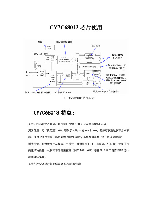
CY7C68013芯片使用图一CY7C68013内部构造CY7C68013特点:支持,内部包括收发器、串行接口引擎(SIE)以及增强型51内核;灵活配置,可“软配置”RAM,取代了传统51的RAM和ROM,程序可以通过以下方式下载:通过USB口下载;通过外部E2PROM装载;外界存储设备(仅128引脚支持)模式灵活,可设置为主从模式,主模式下可对外部FIFO、存储器、ATAn接口设备进行高速读写操作,从模式下外部主控器(例如DSP、MCU)可把GPIF端口当作FIFO进行高速读写操作。
支持与外设通过并行8位或者16位总线传输硬件连接方式在Slave FIFO方式下,外部逻辑与FX2的连接信号图如下:图一从模式下的硬件连接IFCLK:FX2输出的时钟,可做为通讯的同步时钟;FLAGA,FLAGB,FLAGC,FLAGD:FX2输出的FIFO状态信息,如满,空等;SLCS:FIFO的片选信号,外部逻辑控制,当SLCS输出高时,不可进行数据传输;SLOE:FIFO输出使能,外部逻辑控制,当SLOE无效时,数据线不输出有效数据;SLRD:FIFO读信号,外部逻辑控制,同步读时,FIFO指针在SLRD有效时的每个IFCLK 的上升沿递增,异步读时,FIFO读指针在SLRD的每个有效—无效的跳变沿时递增;SLWR:FIFO写信号,外部逻辑控制,同步写时,在SLWR有效时的每个IFCLK的上升沿时数据被写入,FIFO指针递增,异步写时,在SLWR的每个有效—无效的跳变沿时数据被写入,FIFO写指针递增;PKTEND:包结束信号,外部逻辑控制,在正常情况下,外部逻辑向FX2的FIFO中写数,当写入FIFO端点的字节数等于FX2固件设定的包大小时,数据将自动被打成一包进行传输,但有时外部逻辑可能需要传输一个字节数小于FX2固件设定的包大小的包,这时,它只需在写入一定数目的字节后,声明此信号,此时FX2硬件不管外部逻辑写入了多少字节,都自动将之打成一包进行传输;FD[15:0]:数据线;FIFOADR[1:0]:选择四个FIFO端点的地址线,外部逻辑控制。

CY7C68031A固件程序FW.C详解(1)2011-04-01 14:10736人阅读评论(0)收藏举报////本来要一次传上去,百度空间嫌文章太长,只好分为两篇////FW.C文件,我当初看了一个星期,也没看懂的。
这里我们逐字逐句研读,////边理解,边一行一行的注释.////以下是Cypress公司的官方程序,我不做改动,原英文注释保留,只增加注释//简单语句就不说了//// //???//是我不懂得的地方,希望高手补充//// //###//是以后开发可能需要改动的地方//////我加的所有注释都用////四个连斜杠,便于以后不需要的时候屏蔽掉////这是在Keil UV2里编辑的,没有其它格式字符,可以直接编译//-----------------------------------------------------------------------------// File: fw.c// Contents: Firmware frameworks task dispatcher and device request parser //// $Archive: /USB/Examples/FX2LP/bulkext/fw.c $// $Date: 3/23/05 2:53p $// $Revision: 8 $//////-----------------------------------------------------------------------------// Copyright 2003, Cypress Semiconductor Corporation//-----------------------------------------------------------------------------#include "fx2.h"////fx2.h 定义EZUSB的宏、数据类型等的头文件#include "fx2regs.h"////fx2regs.h 定义EZUSB寄存器定义的头文件#include "syncdly.h" // SYNCDELAY macro////syncdly.h同步延时宏定义//-----------------------------------------------------------------------------// Constants//-----------------------------------------------------------------------------#define DELAY_COUNT 0x9248*8L // Delay for 8 sec at 24Mhz, 4 sec at 48 #define _IFREQ 48000 // IFCLK constant for Synchronization Delay#define _CFREQ 48000 // CLKOUT constant for Synchronization Delay////以上设置时钟频率为48MHZ//-----------------------------------------------------------------------------// Random Macros//-----------------------------------------------------------------------------#define min(a,b) (((a)<(b))?(a):(b))#define max(a,b) (((a)>(b))?(a):(b))//-----------------------------------------------------------------------------// Global Variables////全局变量//-----------------------------------------------------------------------------volatile BOOL GotSUD;////GotSUD是令牌包标志,准确的说是“令牌阶段数据到来”,什么是令牌包?////首先,USB一连串的数据传输、处理、响应等就叫做USB事务。
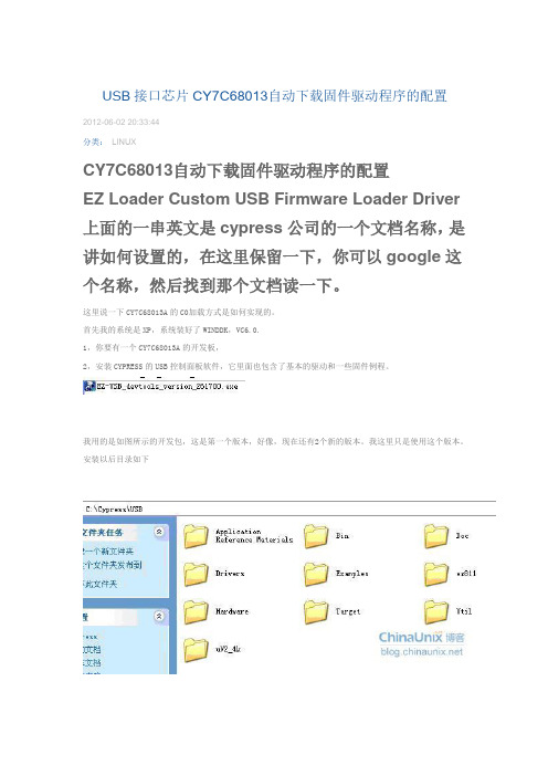
USB接口芯片CY7C68013自动下载固件驱动程序的配置2012-06-02 20:33:44分类:LINUXCY7C68013自动下载固件驱动程序的配置EZ Loader Custom USB Firmware Loader Driver 上面的一串英文是cypress公司的一个文档名称,是讲如何设置的,在这里保留一下,你可以google这个名称,然后找到那个文档读一下。
这里说一下CY7C68013A的C0加载方式是如何实现的。
首先我的系统是XP,系统装好了WINDDK,VC6.0.1,你要有一个CY7C68013A的开发板,2,安装CYPRESS的USB控制面板软件,它里面也包含了基本的驱动和一些固件例程。
我用的是如图所示的开发包,这是第一个版本,好像,现在还有2个新的版本。
我这里只是使用这个版本。
安装以后目录如下然后到drivers目录3,把EZLOADER文件夹,EZUSBDRV文件夹,EZUSBW2K.INF文件,这3个复制到另外的一个文件夹,我这里就直接放在C盘了。
4,从开始菜单,进入到WINDDK的编译环境,是DOS界面,启动它。
到c:\ezloaderok目录目录下文件有:5,用记事本打开Sources文件,将其中的一段修改如下,to build那个英文说得很明白了。
然后回到DOS界面6,输入build –c,如果没有错误编译成功的话,界面如下Ezloader.sys,就是下载固件程序到cy7c68013RAM的驱动文件,说白点就是,它是C0加载方式的,第一个驱动文件,功能就是将固件程序下载到RAM中。
这里差点漏了说,在这之前,我们要把固件程序也就是HEX文件转化为.c 的文件,将这个.c 文件中的那个数组,替换fireware.c 中对应的数组,如图7,成功没有那么容易,我在编译的时候出现了这样的错误,关于USHORT,类型不匹配的错误,找到相应的行,将数据变量强制类型转换,就好了。
之前用的是xp环境,用的红色飓风开发板,现在自己做的板子,改成了win7系统,可是原来的eZ-USB控制面板不能用了,搜了一下cypress的官方驱动,Cypress Suite USB 3.4.7,可以支持XP和win7系统。
连上后,按照driver文件夹下面的CyUSB.pdf文件,修改Cypress Suite USB 3.4.7\Driver\bin\wlh\x64下面的cyusb.inf文件,用记事本打开,将里面VID_XXXX&PID_XXXX改成VID_04B4&PID_8613(在设备管理器中可以查看属性,看到这两个16进制数),注意别忘了把这几行前面的注释号“;”去掉,否则认为这一行被注释了哦。
下面的文件是我的CY7C68013的inf文件。
这样系统就可以识别到USB设备了。
但是原来的例程SlaveFIFO不能用了,下载.hex文件之后,识别到SlaveFIFO设备,不能装驱动。
由于对这个USB芯片的固件不熟,研究固件编写短期内搞不定。
于是在Cypress 官方网站上找到了例程AN63787,是关于8bit模式下的slavefifo例程,但是我的FPGA配置的是16位模式,明显看到例程中少了一半字节的数据。
下面只能自己改例程了。
首先下载**版的keil uVision2,/f/12062296.html?from=like更改C:\Cypress\Cypress Suite USB 3.4.7\Firmware\Bulkloop下面的keil工程,用原来红色飓风自带的固件源代码配置进行更改,将 bulkloop.c中TD_Init函数用红色飓风如下TD_Init函数替换,void TD_Init( void ){ // Called once at startup//时钟设置//CPUCS = 0x02; //12MHZ CLKOUT ENALBE//CPUCS = 0x0a; //24MHZ CLKOUT ENALBECPUCS = 0x12; //48MHZ CLKOUT ENALBEIFCONFIG =0x43;//使用外部时钟,IFCLK输入不反向SYNCDELAY;EP2CFG=0xA0; //需要设定为四缓冲,每个缓冲区大小为512字节SYNCDELAY;EP4CFG=0x00;SYNCDELAY;EP6CFG=0xE0;SYNCDELAY;EP8CFG=0x00;SYNCDELAY;FIFORESET = 0x80; // activate NAK-ALL to avoid race conditionsSYNCDELAY; // see TRM section 15.14FIFORESET = 0x02; // reset, FIFO 2SYNCDELAY; //FIFORESET = 0x06; // reset, FIFO 6SYNCDELAY; //FIFORESET = 0x00; // deactivate NAK-ALLSYNCDELAY;PINFLAGSAB = 0xE6; // FLAGA - fixed EP6PF, FLAGB - fixed EP6FFSYNCDELAY;PINFLAGSCD = 0xf8; // FLAGC - fixed EP2EF, FLAGD - reservedSYNCDELAY;PORTACFG |= 0x00; //0x40; // SLCS, set alt. func. of PA7 pinSYNCDELAY;FIFOPINPOLAR = 0x00; // all signals active low,SYNCDELAY;OEA|=0x0F;//小于64字节有效//EP6FIFOPFH=0x00; //DEIS PKSTAT PK2 PK1 PK0 0 PFC9 PFC8//EP6FIFOPFL=0x40; //PFC7 PFC6 PFC5 PFC4 PFC3 PFC2 PFC1 PFC0// handle the case where we were already in AUTO mode...EP2FIFOCFG = 0x01; // AUTOOUT=0, WORDWIDE=1SYNCDELAY;EP2FIFOCFG = 0x11; // AUTOOUT=1, WORDWIDE=1SYNCDELAY;EP6FIFOCFG = 0x09; // AUTOIN=1, ZEROLENIN=0, WORDWIDE=1SYNCDELAY;//IO设置PORTCCFG=0x00;PORTECFG=0x00;OEC=0x00;OEE=0xff;//串口初始化// PA3=0;PA0=1;enum_high_speed=FALSE;}编译生成.hex文件,用EZ-USB控制面板下载到USB芯片中,然后提示找到设备Bulkloop Device,自动安装驱动,点击get piples,Pipe: 0 Type: BLK Endpoint: 2 OUT MaxPktSize: 0x200Pipe: 1 Type: BLK Endpoint: 4 OUT MaxPktSize: 0x200Pipe: 2 Type: BLK Endpoint: 6 IN MaxPktSize: 0x200Pipe: 3 Type: BLK Endpoint: 8 IN MaxPktSize: 0x200选择: BLK Endpoint: 6 IN ,点击传输,这是我用24bitAD芯片采集数据的结果,每采集两次,放入3个数据进FIFO,数据正确但是现在传输速度测试的VC6.0程序还不能用,估计还是因为win7的某些不兼容吧,以后再试。
CY7C68013A, CY7C68014ACY7C68015A, CY7C68016A EZ-USB FX2LP (TM) USB 微控制器高速 USB 外设控制器1. 特色 (CY7C68013A/14A/15A/16A)■USB 2.0 USB IF 高速性能且经过认证 (TID # 40460272)■单芯片集成 USB 2.0 收发器、智能串行接口引擎 (SIE) 和增强型 8051 微处理器■适用性、外观和功能均与FX2兼容❐引脚兼容❐目标代码兼容❐功能兼容(FX2LP 是超集)■超低功耗:I CC在任何模式下都不超过 85 mA❐适合总线和电池供电的应用■软件:8051 代码运行介质:❐内部 RAM,通过 USB 下载❐内部 RAM,从 EEPROM 加载❐外部存储设备(128 引脚封装)■16 K 字节片上代码/数据 RAM■四个可编程的 BULK/INTERRUPT/ISOCHRONOUS 端点❐缓冲区大小选项:两倍,三倍,四倍■附加的可编程(BULK/INTERRUPT) 64 位端点■8 位或 16 位外部数据接口■可生成智能介质标准错误校正码 ECC ■通用可编程接口 (General Programmable Interface,GPIF)❐可与大多数并行接口直接连接❐由可编程波形描述符和配置寄存器定义波形❐支持多个 Ready (RDY) 输入和 Control (CTL) 输出■符合行业标准的集成增强型 8051❐48 MHz、24 MHz 或 12 MHz CPU 操作❐每个指令周期四个时钟❐两个 USART❐三个计数器/定时器❐扩展的中断系统❐两个数据指针■3.3V 工作电压,容限输入为 5V■向量化 USB 中断和 GPIF/FIFO 中断■分离的 CONTROL 传输设置部分和数据部分数据缓冲■集成 I2C 控制器,在 100 或 400 kHz 下运行■集成的四个先进先出 (FIFO) 缓冲❐集成胶合逻辑和 FIFO 有助于降低系统成本❐与 16 位总线之间的自动转换❐可主-从操作❐使用外部时钟或异步选通脉冲❐易于与 ASIC 和 DSP IC 相连的接口■有商业和工业温度等级供选择(除 VFBGA 外的所有封装)1.1 特色(仅限 CY7C68013A/14A )■CY7C68014A :适合电池供电应用❐挂起电流:100 μA (typ)■CY7C68013A :适合非电池供电应用❐挂起电流:300 μA (typ)■有五种无铅封装供选择,可包含多达 40 个 GPIO ❐128 引脚 TQFP (40 个 GPIO )、100 引脚 TQFP (40 个 GPIO )、56 引脚 QFN (24 个 GPIO )、56 引脚 SSOP (24 个 GPIO )和 56 引脚 VFBGA (24 个 GPIO )1.2 特色(仅限 CY7C68015A/16A )■CY7C68016A :适合电池供电应用❐挂起电流:100 μA (typ)■CY7C68015A :适合非电池供电应用❐挂起电流:300 μA (typ)■采用无铅 56 引脚 QFN 封装(26 个 GPIO )❐比 CY7C68013A/14A 多 2 个 GPIO ,可在同样的空间内实现额外的功能赛普拉斯半导体公司(赛普拉斯)的 EZ-USB FX2LP ™ (CY7C68013A/14A) 是高集成、低功耗 USB 2.0 微控制器EZ-USB FX2™ (CY7C68013) 的一个低功耗版本。
EZ-USBFX2(68013)Cmos摄像头研究laveFIFO固件感觉固件要写的东西还是比较少的,主要是SlaveFIFO的配置。
使用端点2,in 传输,端点描述符为:db DSCR_ENDPNT_LEN ;; Descriptor lengthdb DSCR_ENDPNT ;; Descriptor typedb 82H ;; Endpoint number, and direction db ET_BULK ;; Endpoint typedb 00H ;; Maximun packet size (LSB)db 02H ;; Max packect size (MSB)db 00H ;; Polling interval在这里将最大包设为512bytes。
然后就是初始化时的SLaveFIFO 配置,同步,AUTO IN,端点2,基本上是TRM中的实例,稍作修改,需要注意的是特殊寄存器连续设置时要延时SYNCDELAY,TRM中的代码有两处好像掉了,我当初照着弄的时候就有问题,后来加上就好了。
设置CLKOUT输出驱动Sensor:CPUCS = ((CPUCS & ~bmCLKSPD) | bmCLKSPD1|bmCLKOE) ;其他的地方参照TRM的9.3.10的例子,代码我就不贴了.我是将端点8改为2。
其他配置也采用端点2的配置,另外端点2设置为512×4倍缓冲,有个问题就是我如果设置为1024的话,会出错,不知道为什么?看网上好多设为1024的也是类似问题,貌似是cypress的驱动不支持1024.接下来就是sensor部分的初始化,主要是对snesor寄存器参数配置;这里就有个问题了,EZUSB提供的I2C函数,ReadI2C真不知道咋用,汗!看好多人也是这问题,读到的数都是错误的。
没办法,只能操作I2C那三个寄存器了。
郁闷,Cypress也写的不清不楚的。
最后就是Vendor命令中的处理了,在接收到上位机开始采集一帧图像的Vendor命令后,反复查询,知道VSYNC信号的到来,马上清空FIFO,然后返回,保证一帧图像的完整性。
CY7C68013A SLAVE FIFO接口设计[简介][作者:Neo][Email:Jei_robot@]简要记录68013A使用要点版本:V100主要内容:1、CY7C68013A16位接口原理图2、固件设计3、API接口1.原理图下图为16位数据总线的原理图。
图:68013A16位原理图1.1图中FM24CL64为铁电IIC接口存储器,用于存储68013A的固件代码(在本例中实际固件代码大约为3K),掉电保存。
关于外部存储器的设计,手册有如下要求:在参考原理图中使用的是24CL64兼容产品,所以根据要求A0地址线拉高,其余为低。
1.2时钟信号使用的是24MHz有源晶振1.3关键信号说明68013A管脚15USB数据线D+16USB数据线D-38FLAGC在本次应用中配置为FIFO空标志37FLAGB在本次应用中配置为FIFO满标志44/45总线地址A0,A149USB芯片复位,重新连接参考原理图16位数据总线(软件也可配置为8位)47USB CS总线选择信号,低电平有效9总线写数据8总线读数据46数据包强制发送(当发送数据不足512字节时需要用到)40USB连接状态指示LED20暂未使用2.固件改写68013A固件下载cypress提供的标准开发工具,其中包括slave fifo测试代码。
只需要简单改写即可应用。
其中主要改写函数是:TD_Init(void).//-----------------------------------------------------------------------------//Task Dispatcher hooks//The following hooks are called by the task dispatcher.//-----------------------------------------------------------------------------void TD_Init(void)//Called once at startup{CPUCS=0x10;//CLKSPD[1:0]=10,for48MHz operationSYNCDELAY;REVCTL=0x03;SYNCDELAY;IFCONFIG=0xCB;SYNCDELAY;FIFOPINPOLAR=0x00;//all signals active lowSYNCDELAY;//EP2512BULK OUT4xEP2CFG=0xA0;//BUF[1:0]=00for4x buffering//EP6512BULK IN4xSYNCDELAY;//EP6CFG=0xE0;//BUF[1:0]=00for4x buffering//EP4and EP8are not used in this implementation...SYNCDELAY;//EP4CFG=0x20;//clear valid bitSYNCDELAY;//EP8CFG=0x60;//clear valid bitSYNCDELAY;FIFORESET=0x80;//activate NAK-ALL to avoid race conditions SYNCDELAY;//see TRM section15.14FIFORESET=0x02;//reset,FIFO2SYNCDELAY;//FIFORESET=0x04;//reset,FIFO4SYNCDELAY;//FIFORESET=0x06;//reset,FIFO6SYNCDELAY;//FIFORESET=0x08;//reset,FIFO8SYNCDELAY;//FIFORESET=0x00;//deactivate NAK-ALL//handle the case where we were already in AUTO mode...//...for example:back to back firmware downloads...SYNCDELAY;//EP2FIFOCFG=0x00;//AUTOOUT=0,8bit data bus//core needs to see AUTOOUT=0to AUTOOUT=1switch to arm endp'sSYNCDELAY;OUTPKTEND=0x02;SYNCDELAY;OUTPKTEND=0x02;SYNCDELAY;OUTPKTEND=0x02;SYNCDELAY;OUTPKTEND=0x02;SYNCDELAY;//EP2FIFOCFG=0x10;//AUTOOUT=1,8bit data busEP2FIFOCFG=0x11;//AUTOOUT=1,16bit data busSYNCDELAY;////EP6FIFOCFG=0x0C;//AUTOIN=1,ZEROLENIN=1,WORDWIDE=18bit data bus EP6FIFOCFG=0x0D;//AUTOIN=1,ZEROLENIN=1,WORDWIDE=116bit data bus SYNCDELAY;//flag B:full,flag C:empty//EP2bulk out;Slaver receive data//EP6bulk in;Slaver send dataPINFLAGSAB=0x80;//FLAGA-PF;FLAGB-FF;FLAGC-EF;FLAGD-PF SYNCDELAY;//FLAGB-EP2EMPTYPINFLAGSCD=0x0E;SYNCDELAY;//FLAGC-EP6FULL//使能CSSYNCDELAY;PORTACFG&=~0X80;SYNCDELAY;PORTACFG|=0x40;//USB连接指示灯SYNCDELAY;OEA|=0x1;//enable PA0output,for USB LEDSYNCDELAY;PA0=0;//USB LED}ARM读写本文测试板采用的是ARM+68013A,ARM端正确配置总线读写接口之后,读写68013A FIFO 代码参考如下:/**写两个字节到68013A fifo*/INT16U cy68013_SendFifo(INT16U data){*((INT16U*)(CY68013_WRITE_ADDR))=data;return(data);}/**读取两个字节*/INT16U cy68013_GetWord(void){return*((INT16U*)(CY68013_READ_ADDR));}3.API接口API的设计最主要的参考文档是官方开发工具中的:CyAPI.chm.本次开发使用的是VC6开发环境,下面的例程是打开一个USB设备,读写数据//打开设备//Look for a device having VID=0547,PID=1002USBDevice=new CCyUSBDevice(Handle);//Create an instance of CCyUSBDevice int devices=USBDevice->DeviceCount();int vID,pID;int d=0;do{USBDevice->Open(d);//Open automatically calls Close()if necessaryvID=USBDevice->VendorID;pID=USBDevice->ProductIDd++;}while((d<devices)&&(vID!=0x0547)&&(pID!=0x1002));//发送数据if(true!=USBDevice->IsOpen()){AfxMessageBox("Sorry!Device is not open!",0);return FALSE;}LONG length=512;UCHAR Buf[512];ZeroMemory(Buf,512);if(size>512)size=512;memcpy(Buf,p,size);OVERLAPPED outOvLap;outOvLap.hEvent=CreateEvent(NULL,false,false,"CYUSB_OUT");//Just to be cute,request the return data before initiating the loopbackUCHAR*outContext=USBDevice->BulkOutEndPt->BeginDataXfer(Buf,length,&outOvLap);bool result=USBDevice->BulkOutEndPt->WaitForXfer(&outOvLap,800);USBDevice->BulkOutEndPt->FinishDataXfer(Buf,length,&outOvLap,outContext);CloseHandle(outOvLap.hEvent);return result;//读取数据if(true!=USBDevice->IsOpen()){AfxMessageBox("Sorry!Device is not open!",0);return FALSE;}LONG length=512;OVERLAPPED inOvLap;inOvLap.hEvent=CreateEvent(NULL,false,false,"CYUSB_IN");//Just to be cute,request the return data before initiating the loopbackUCHAR*inContext=USBDevice->BulkInEndPt->BeginDataXfer(p,length,&inOvLap);bool result=USBDevice->BulkInEndPt->WaitForXfer(&inOvLap,800);USBDevice->BulkInEndPt->FinishDataXfer(p,length,&inOvLap,inContext);CloseHandle(inOvLap.hEvent);*size=512;return result;。
68013有三种EEPROM引导加载方式
1.无EEPROM或EEPROM无效
2."C0"EEPROM加载
3."C2"EEPROM加载
上电之后,FX2检测到有一个EEPROM连接在I2C总线上,并且地址0上的数据值为
0xC2,则FX2会将EEPROM中的数据加载到内部RAM中.然后运行价载的程序. EEPROM中前八个字节格式:
0:0xC2
1:VIDL制造商ID
2:VIDH
3:PIDL产品ID
4:PIDH
5:DIDL设备ID
6:DIDH
7:设置字节
8:长度(高字节)
9:长度(低字节)
10:开始地址(高字节)
11:开始地址(低地址)
...............
...............
N-4:0x80
N-3:0x01
N-2:0xE6
N-1:0x00
N:0x00
可用Hex2bix.exe生成一个iic文件,根据用户输入可生成以上格式的iic文件,如
C:\Cypress\USB\Bin>hex2bix -i -f 0xc2 -v <VID> -p <PID> -o iicfilename.iic hexfilename.hex
关于Hex2bix.exe的具体用法,可用”Hex2bix -help“察看。
Intel Hex file to EZ-USB Binary file conversion utility
Copyright (c) 1997-1999, Cypress Semiconductor Inc.
HEX2BIX [-AIBRH?] [-S symbol] [-M memsize] [-C Config0Byte] [-F firstByte] [-O filename] Source
Source - Input filename
A - Output file in the A51 file format
B - Output file in the BIX file format (Default)
BI - Input file in the BIX file format (hex is default)
C - Config0 BYTE for AN2200 and FX2 (Default = 0x04)
F - First byte (0xB0, 0xB2, 0xB6, 0xC0, 0xC2) (Default = 0xB2) H|? - Display this help screen
I - Output file in the IIC file format
M - Maximum memory size, also used as BIX out file size. (Default = 8k)
O - Output filename
P - Product ID (Default = 2131)
R - Append bootload block to release reset
S - Public symbol name for linking
V - Vendor ID (Default = 0x0547)。