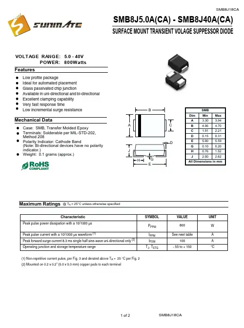
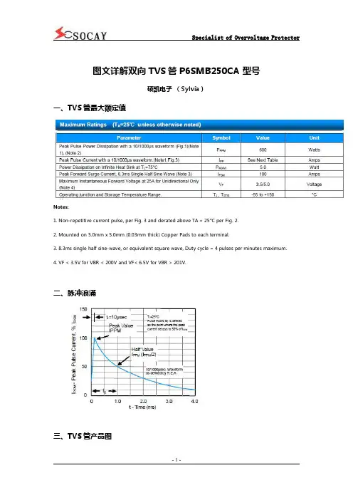
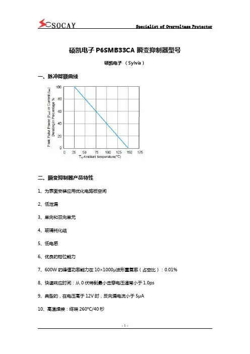
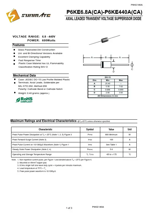
P6SMB18CAT3资料
- 格式:pdf
- 大小:73.83 KB
- 文档页数:6
© Semiconductor Components Industries, LLC, 2006July, 2006 − Rev. 81Publication Order Number:P6SMB11CAT3/DP6SMB11CAT3 Series
600 Watt Peak Power ZenerTransient Voltage SuppressorsBidirectional*The SMB series is designed to protect voltage sensitivecomponents from high voltage, high energy transients. They haveexcellent clamping capability, high surge capability, low zenerimpedance and fast response time. The SMB series is supplied inON Semiconductor’s exclusive, cost-effective, highly reliableSurmetict package and is ideally suited for use in communicationsystems, automotive, numerical controls, process controls, medicalequipment, business machines, power supplies and many otherindustrial/consumer applications.Features•Working Peak Reverse Voltage Range − 9.4 to 77.8 V•Standard Zener Breakdown Voltage Range − 11 to 91 V•Peak Power − 600 W @ 1 ms•ESD Rating of Class 3 (>16 KV) per Human Body Model•Maximum Clamp Voltage @ Peak Pulse Current•Low Leakage < 5 mA Above 10 V•UL 497B for Isolated Loop Circuit Protection•Response Time is Typically < 1 ns•Pb−Free Packages are AvailableMechanical Characteristics:CASE: Void-Free, Transfer-Molded, Thermosetting PlasticFINISH: All External Surfaces are Corrosion Resistant and Leads areReadily SolderableMAXIMUM CASE TEMPERATURE FOR SOLDERING PURPOSES:260°C for 10 SecondsLEADS: Modified L−Bend Providing More Contact Area to Bond PadsPOLARITY: Polarity Band Will Not be IndicatedMOUNTING POSITION: AnyMAXIMUM RATINGSRatingSymbolValueUnitPeak Power Dissipation (Note 1) @ TL = 25°C,Pulse Width = 1 msPPK600WDC Power Dissipation @ TL = 75°CMeasured Zero Lead Length (Note 2)Derate Above 75°CThermal Resistance, Junction−to−LeadPDRqJL3.04025WmW/°C°
C/WDC Power Dissipation (Note 3) @ TA = 25°CDerate Above 25°CThermal Resistance, Junction−to−AmbientPDRqJA0.554.4226WmW/°C°C/W
Operating and Storage Temperature RangeTJ, T
stg−65 to+150°CStresses exceeding Maximum Ratings may damage the device. MaximumRatings are stress ratings only. Functional operation above the RecommendedOperating Conditions is not implied. Extended exposure to stresses above theRecommended Operating Conditions may affect device reliability.1.10 X 1000 ms, non−repetitive2.1″ square copper pad, FR−4 board3.FR−4 board, using ON Semiconductor minimum recommended footprint, asshown in 403A case outline dimensions spec.*Please see P6SMB6.8AT3 to P6SMB200AT3 for Unidirectional devices.PLASTIC SURFACE MOUNTZENER OVERVOLTAGETRANSIENT SUPPRESSORS9.4−78 VOLTS600 WATT PEAK POWER
Devices listed in bold, italic are ON SemiconductorPreferred devices. Preferred devices are recommendedchoices for future use and best overall value.DevicePackageShipping†ORDERING INFORMATION
P6SMBxxCAT3SMB2500/Tape & ReelSMBCASE 403APLASTIC
MARKING DIAGRAMhttp://onsemi.com
AYWWxxCGG
xxC= Device CodeA= Assembly LocationY= YearWW= Work WeekG= Pb−Free Package(Note: Microdot may be in either location)
P6SMBxxCAT3GSMB(Pb−Free)2500/Tape & Reel
†For information on tape and reel specifications,including part orientation and tape sizes, pleaserefer to our Tape and Reel Packaging SpecificationsBrochure, BRD8011/D.The “T3” suffix refers to a 13 inch reel.元器件交易网www.cecb2b.com
Bi−Directional TVSIPPIPP
VI
IRITITIRVRWMVCVBRVRWMVCVBRP6SMB11CAT3 Series
http://onsemi.com2ELECTRICAL CHARACTERISTICS(TA = 25°C unless otherwise noted)SymbolParameterIPPMaximum Reverse Peak Pulse CurrentVCClamping Voltage @ IPPVRWMWorking Peak Reverse VoltageIRMaximum Reverse Leakage Current @ VRWMVBRBreakdown Voltage @ ITITTest CurrentQVBRMaximum Temperature Coefficient of VBR
ELECTRICAL CHARACTERISTICS (Devices listed in bold, italic are ON Semiconductor Preferred devices.)
Device*DeviceMarkingVRWM(Note 4)IR @VRWMBreakdown VoltageVC @ IPP (Note 6)QVBRCtyp(Note 7)VBR Volts (Note 5)@ ITVCIPPVoltsmAMinNomMaxmAVoltsAmps%/°CpFP6SMB11CAT3, GP6SMB12CAT3, GP6SMB13CAT3, G11C12C13C9.410.211.155510.511.412.411.051213.0511.612.613.711115.616.718.23836330.0750.0780.081865800740P6SMB15CAT3, GP6SMB16CAT3, GP6SMB18CAT3, GP6SMB20CAT3, G15C16C18C20C12.813.615.317.1555514.315.217.11915.0516182015.816.818.921111121.222.525.227.7282724220.0840.0860.0880.09645610545490P6SMB22CAT3, GP6SMB24CAT3, GP6SMB27CAT3, GP6SMB30CAT3, G22C24C27C30C18.820.523.125.6555520.922.825.728.5222427.053023.125.228.431.5111130.633.237.541.420181614.40.090.0940.0960.097450415370335P6SMB33CAT3, GP6SMB36CAT3, GP6SMB39CAT3, GP6SMB43CAT3, G33C36C39C43C28.230.833.336.8555531.434.237.140.933.053639.0543.0534.737.84145.2111145.749.953.959.313.21211.210.10.0980.0990.10.101305280260240P6SMB47CAT3, GP6SMB51CAT3, GP6SMB56CAT3, GP6SMB62CAT3, G47C51C56C62C40.243.647.853555544.748.553.258.947.0551.05566249.453.658.865.1111164.870.177859.38.67.87.10.1010.1020.1030.104220205185170P6SMB68CAT3, GP6SMB75CAT3, GP6SMB82CAT3, GP6SMB91CAT3, G68C75C82C91C58.164.170.177.8555564.671.377.986.56875.05829171.478.886.195.51111921031131256.55.85.34.80.1040.1050.1050.1061551401301204.A transient suppressor is normally selected according to the working peak reverse voltage (VRWM), which should be equal to or greater thanthe DC or continuous peak operating voltage level.5.VBR measured at pulse test current IT at an ambient temperature of 25°C.6.Surge current waveform per Figure 2 and derate per Figure 3 of the General Data − 600 Watt at the beginning of this group.7.Bias Voltage = 0 V, F = 1 MHz, TJ = 25°C*The “G’’ suffix indicates Pb−Free package available. Please refer back to Ordering Information on front page.元器件交易网www.cecb2b.com