IR17-21CTR8, 规格书,Datasheet 资料
- 格式:pdf
- 大小:254.03 KB
- 文档页数:10
光耦电路设计目录简介:输入电路(原边)输出电路(副边)电流传输比:延时:简介:外部信号可能是电压、电流或开关触点,直接接入电路可能会引起瞬时高压、过压、接触点抖动等。
因此在外部信号输入之前,须经过转换、保护、滤波、隔离等措施。
对小功率信号处理时: 通常简单采用RC 积分滤波或再添加门电路;而在对大功率信号处理时:输入与内部电路电压或电源电压的压差较大,常常采用光电耦合器来隔离。
使用光耦设计隔离电路时,特别要注意电流传输比的降额,驱动电流关断和开通的大小,与延迟相关的负载大小及开关速率。
在进行光耦输入电路设计时,是以光耦为中心的输入电路与输出电路(即原边与副边的电路),光耦的工作原理就是输入端输入信号V in,光耦原边二极管发光使得光耦副边的光敏三极管导通,三极管导通形成回路产生相应信号(电压或者电流),这样就实现传递信号的目的。
在进行光耦输出电路设计时,计算公式与输入部分相同,同时需关注电平匹配、阻抗匹配、驱动功率、负载类型和大小。
以下针对光耦输入电路设计为例。
图1 LED驱动电路输入电路(原边):针对于光耦原边的电路设计,如图1 ,就是设计发光二级管的驱动电路。
因此须首先要了解光耦的原边电流I F和二极管的导通压降V F等相关信息。
根据必要的信息来设计LED驱动电路,和通常的数字输入电路一样,输入端需要添加限流电阻对二极管起保护作用。
而这个电阻的阻值则是此处的关键,对于图1的限流电阻R的阻值可以根据下面的公式计算:……………………… ①基于对抗干扰能力的考虑,通常在靠近光耦的原边并联接入一个电容进行滤波。
并且RC电路的延迟特性也可以达到测试边沿,产生硬件死区、消除抖动等益处。
同时在数字电路中其延迟特性可能会影响到信号的同步问题(尤其是通讯、异步电路、使能控制等),因此要充分注意电路的时间约束。
根据设计要求,为了确保输入端和公共端的电压差Vin在4V以下时,输入无效,光耦断开。
为此我们在输入端与公共端之间并接一个电阻避免输入无效时造成光耦原边的误导通。

元器件交易网EVERLIGHT ELECTRONICS CO.,LTD.Technical Data Sheet 0805 Package Chip LED (1.0m Height)17-21SURC/S530-XX/TR8Features․Package in 8mm tape on 7〞diameter reel. ․Compatible with automatic placement equipment. ․Compatible with infrared and vapor phase reflow solder process. ․Mono-color type. ․Pb-free. ․The product itself will remain with in RoHS complaint versionDescriptions․The 17-21 SMD Taping is much smaller than lead frame type components, thus enable smaller board size, higher packing density, reduced storage space and finally smaller equipment to be obtained. ․Besides, lightweight makes them ideal for miniature applications. etc.Applications․Backlighting in dashboard and switch. ․Telecommunication: indicator and backlighting in telephone and fax. ․Flat backlight for LCD, switch and symbol. ․General use.Device Selection GuidePart No. 17-21SURC/S530-XX/TR8 Chip Material AlGaInP Emitted Color Brilliant Red Resin Color Water ClearEverlight Electronics Co., Ltd. Device No:SZDSE-171-019 Prepared date: 27-Oct-2007Rev. 2Page: 1 of 9Prepared by: Zhouhua元器件交易网EVERLIGHT ELECTRONICS CO.,LTD.17-21SURC/S530-XX/TR8Package Outline Dimensions-+1.05Note: The tolerances unless mentioned is ±0.1mm,Unit = mmEverlight Electronics Co., Ltd. Device No:SZDSE-171-019 Prepared date: 27-Oct-2007Rev. 2Page: 2 of 9Prepared by: Zhouhua元器件交易网EVERLIGHT ELECTRONICS CO.,LTD.17-21SURC/S530-XX/TR8Absolute Maximum Ratings (Ta=25℃)Parameter Reverse Voltage Forward Current Peak Forward Current (Duty 1/10 @1KHz) Power Dissipation Electrostatic Discharge(HBM) Operating Temperature Storage Temperature Soldering Temperature Symbol VR IF IFP Pd ESD Topr Tstg Tsol Rating 5 25 60 60 2000 -40 ~ +85 -40 ~ +90 Unit V mA mA mW V ℃ ℃Reflow Soldering:260 ℃ for 10 sec Hand Soldering:350℃ for 3 secElectro-Optical Characteristics (Ta=25℃)Parameter Symbol *Chip Rank Min. Typ. Max. Unit ConditionLuminous IntensityIvA2 A3 A4 A5 A6 -------------------------15 40 50 60 85 -------------------------38 60 75 90 123 140 632 624 20 2.0 -----------------------------------------2.4 10mcdViewing Angle Peak WavelengthDominant Wavelength2θ1/2 λp λd △λ VF IRdeg nm nm nm V μAIF=20 mASpectrum Radiation Bandwidth Forward VoltageReverse CurrentVR=5VEverlight Electronics Co., Ltd. Device No:SZDSE-171-019 Prepared date: 27-Oct-2007Rev. 2Page: 3 of 9Prepared by: Zhouhua元器件交易网EVERLIGHT ELECTRONICS CO.,LTD.17-21SURC/S530-XX/TR8Typical Electro-Optical Characteristics CurvesEverlight Electronics Co., Ltd. Device No:SZDSE-171-019 Prepared date: 27-Oct-2007Rev. 2Page: 4 of 9Prepared by: Zhouhua元器件交易网EVERLIGHT ELECTRONICS CO.,LTD.17-21SURC/S530-XX/TR8Label explanationCAT: Luminous Intensity Rank HUE: Dom. Wavelength Rank REF: Forward Voltage Rankxxxxxx xxxxxxRoHSxxxxxxxxxxxx xxxx xxxxxxxxReel DimensionsNote: The tolerances unless mentioned is ±0.1mm ,Unit = mmEverlight Electronics Co., Ltd. Device No:SZDSE-171-019 Prepared date: 27-Oct-2007Rev. 2Page: 5 of 9Prepared by: Zhouhua元器件交易网EVERLIGHT ELECTRONICS CO.,LTD.17-21SURC/S530-XX/TR8Carrier Tape Dimensions: Loaded quantity 3000 PCS per reelNote: The tolerances unless mentioned is ±0.1mm ,Unit = mmMoisture Resistant PackagingLabelAluminum moisture-proof bagDesiccantLabelEverlight Electronics Co., Ltd. Device No:SZDSE-171-019 Prepared date: 27-Oct-2007Rev. 2Page: 6 of 9Prepared by: Zhouhua元器件交易网EVERLIGHT ELECTRONICS CO.,LTD.17-21SURC/S530-XX/TR8Reliability Test Items And ConditionsThe reliability of products shall be satisfied with items listed below. Confidence level:90% LTPD:10%No. 1Items Reflow SolderingTest Condition Temp. : 260℃±5℃ Min. 5sec. H : +100℃ 15min ∫ 5 min L : -40℃ 15min H : +100℃ 5min ∫ 10 sec L : -10℃ 5min Temp. : 100℃ Temp. : -40℃ IF = 20 mA 85℃/ 85%RHTest Sample Hours/Cycles Size 6 Min. 300 Cycles 22 PCS.Ac/Re 0/12Temperature Cycle22 PCS.0/13Thermal Shock High Temperature Storage Low Temperature Storage DC Operating Life High Temperature / High Humidity300 Cycles 1000 Hrs. 1000 Hrs. 1000 Hrs. 1000 Hrs.22 PCS.0/14 5 6 722 PCS. 22 PCS. 22 PCS. 22 PCS.0/1 0/1 0/1 0/1Everlight Electronics Co., Ltd. Device No:SZDSE-171-019 Prepared date: 27-Oct-2007Rev. 2Page: 7 of 9Prepared by: Zhouhua元器件交易网EVERLIGHT ELECTRONICS CO.,LTD.17-21SURC/S530-XX/TR8Precautions For Use1. Over-current-proof Customer must apply resistors for protection , otherwise slight voltage shift will cause big current change ( Burn out will happen ). 2. Storage 2.1 Do not open moisture proof bag before the products are ready to use. 2.2 Before opening the package, the LEDs should be kept at 30℃ or less and 90%RH or less. 2.3 After opening the package: The LED's floor life is 1 year under 30℃or less and 60% RH orless. If unused LEDs remain, it should be stored in moisture proof packages. 2.4 If the moisture absorbent material (silica gel) has faded away or the LEDs have exceeded the storage time, baking treatment should be performed using the following conditions. Baking treatment : 60±5℃ for 24 hours. 3. Soldering Condition 3.1 Pb-free solder temperature profile3.2 Reflow soldering should not be done more than two times. 3.3 When soldering, do not put stress on the LEDs during heating. 3.4 After soldering, do not warp the circuit board.Everlight Electronics Co., Ltd. Device No:SZDSE-171-019 Prepared date: 27-Oct-2007Rev. 2Page: 8 of 9Prepared by: Zhouhua元器件交易网EVERLIGHT ELECTRONICS CO.,LTD.17-21SURC/S530-XX/TR84. Soldering Iron Each terminal is to go to the tip of soldering iron temperature less than 350℃ for 3 seconds within once in less than the soldering iron capacity 25W. Leave two seconds and more intervals, and do soldering of each terminal. Be careful because the damage of the product is often started at the time of the hand solder.5.Repairing Repair should not be done after the LEDs have been soldered. When repairing is unavoidable, a double-head soldering iron should be used (as below figure). It should be confirmed beforehand whether the characteristics of the LEDs will or will not be damaged by repairing.EVERLIGHT ELECTRONICS CO., LTD. Office: No 25, Lane 76, Sec 3, Chung Yang Rd, Tucheng, Taipei 236, Taiwan, R.O.CTel: 886-2-2267-2000, 2267-9936 Fax: 886-2267-6244, 2267-6189, 2267-6306 Everlight Electronics Co., Ltd. Device No:SZDSE-171-019 Prepared date: 27-Oct-2007Rev. 2Page: 9 of 9Prepared by: Zhouhua。

ir2117strpbf规格书
(原创版)
目录
1.产品概述
2.产品规格
3.功能特性
4.应用领域
5.安全与环保
6.客户支持
正文
【产品概述】
ir2117strpbf 是一款高性能、低功耗的电源管理芯片,适用于各种电子设备和系统。
该芯片的设计旨在为用户提供可靠、高效的电源解决方案,满足现代电子产品对能源管理的高要求。
【产品规格】
ir2117strpbf 的规格如下:
- 输入电压范围:3.3V to 5V
- 输出电压范围:1.8V to 5.5V
- 最大输出电流:3A
- 工作温度范围:-40°C to +85°C
- 封装形式:SOP-8
【功能特性】
ir2117strpbf 具有以下功能特性:
- 高效率:在轻载条件下,该芯片的效率可达到 90% 以上,有助于降低系统功耗。
- 输出电压可调:用户可通过调整外部电阻来设定输出电压,以满足不同应用场景的需求。
- 短路保护:芯片内置短路保护功能,可在短路发生时快速切断输出,保护电路安全。
- 过温保护:当芯片温度超过设定值时,会自动切断输出,以防止过热损坏。
【应用领域】
ir2117strpbf 广泛应用于各种电子设备和系统中,如:
- 移动通信设备
- 消费类电子产品
- 工业控制设备
- 电脑周边设备
【安全与环保】
ir2117strpbf 在设计和生产过程中严格遵循国家和行业的安全与环保标准,确保产品在使用过程中对用户和环境无害。

Dimensions: [mm]2112Scale - 3:1Würth Elektronik eiSos GmbH & Co. KG EMC & Inductive Solutions Max-Eyth-Str. 174638 Waldenburg Germany140817141210Würth Elektronik eiSos GmbH & Co. KGEMC & Inductive Solutions140817141210 Max-Eyth-Str. 174638 WaldenburgGermanyTotal Power Dissipation vs. Ambient Temperature:20406080100120140160-55-35-15525456585105125IR-diode -I F(mA)Ambient Temperature (°C)Phototransistor-PO(mW)CollectorPowerDissipation(mW)ForwardCurrent(mA)Collector Dark Current vs. Ambient Temperature:11010010001000025456585105125CollectorDarkCurrent(nA)Ambient Temperature (°C)V CE= 20VV CE= 10VNote: measured with Bin BWürth Elektronik eiSos GmbH & Co. KGEMC & Inductive SolutionsMax-Eyth-Str. 174638 WaldenburgGermanyCHECKED REVISION DATE (YYYY-MM-DD)GENERAL TOLERANCE PROJECTIONMETHODSaVo001.0052023-08-22DIN ISO 2768-1mDESCRIPTIONWL-OCPT OptocouplerPhototransistor ORDER CODE140817141210SIZE/TYPE BUSINESS UNIT STATUS PAGEAbsolute CTR vs. Ambient Temperature50100150200250300-60-40-20020406080100120AbsoluteCTRAmbient Temperature (°C)V CE= 5VV CE= 0,4VTestcondition: I F=5mA, T A=25°C, Bin BRelative CTR vs. Ambient Temperature:0,40,60,811,21,4-60-40-20020406080100120RelativeCTRAmbient Temperature (°C)V CE= 5VV CE= 0,4VTestcondition: I F=5mA, Normalized to T A=25°C, Bin BWürth Elektronik eiSos GmbH & Co. KGEMC & Inductive SolutionsMax-Eyth-Str. 174638 WaldenburgGermanyCHECKED REVISION DATE (YYYY-MM-DD)GENERAL TOLERANCE PROJECTIONMETHODSaVo001.0052023-08-22DIN ISO 2768-1mDESCRIPTIONWL-OCPT OptocouplerPhototransistor ORDER CODE140817141210SIZE/TYPE BUSINESS UNIT STATUS PAGEWürth Elektronik eiSos GmbH & Co. KGEMC & Inductive Solutions140817141210 Max-Eyth-Str. 174638 WaldenburgGermanyWürth Elektronik eiSos GmbH & Co. KGEMC & Inductive Solutions140817141210 Max-Eyth-Str. 174638 WaldenburgGermany050100150200250300350400450A b s o l u t e C T R (%)Testcondition T A Würth Elektronik eiSos GmbH & Co. KG EMC & Inductive Solutions Max-Eyth-Str. 174638 Waldenburg Germany140817141210050100150200250300A b s o l u t e C T R (%)Testcondition T A Würth Elektronik eiSos GmbH & Co. KG EMC & Inductive Solutions Max-Eyth-Str. 174638 Waldenburg Germany1408171412100102030R e s p o n s e T i m e (µs )Testcondition I C Würth Elektronik eiSos GmbH & Co. KG EMC & Inductive Solutions Max-Eyth-Str. 174638 Waldenburg Germany140817141210Würth Elektronik eiSos GmbH & Co. KGEMC & Inductive Solutions140817141210 Max-Eyth-Str. 174638 WaldenburgGermanyWürth Elektronik eiSos GmbH & Co. KGEMC & Inductive Solutions140817141210 Max-Eyth-Str. 174638 WaldenburgGermanyT e m p e r a t u r eT T T Würth Elektronik eiSos GmbH & Co. KG EMC & Inductive Solutions Max-Eyth-Str. 174638 Waldenburg Germany140817141210Cautions and Warnings:The following conditions apply to all goods within the product series of Optoelectronic Components of Würth Elektronik eiSos GmbH & Co. KG:General:•This optoelectronic component is designed and manufactured for use in general electronic equipment.•Würth Elektronik must be asked for written approval (following the PPAP procedure) before incorporating the components into any equipment in fields such as military, aerospace, aviation, nuclear control, submarine, transportation (automotive control, train control,ship control), transportation signal, disaster prevention, medical, public information network, etc. where higher safety and reliability are especially required and/or if there is the possibility of direct damage or human injury.•Optoelectronic components that will be used in safety-critical or high-reliability applications, should be pre-evaluated by the customer. •The optoelectronic component is designed and manufactured to be used within the datasheet specified values. If the usage and operation conditions specified in the datasheet are not met, the wire insulation may be damaged or dissolved. •Do not drop or impact the components, the component may be damaged•Würth Elektronik products are qualified according to international standards, which are listed in each product reliability report. Würth Elektronik does not warrant any customer qualified product characteristics beyond Würth Elektroniks’ specifications, for its validity and sustainability over time.•The responsibility for the applicability of the customer specific products and use in a particular customer design is always within the authority of the customer. All technical specifications for standard products also apply to customer specific products.•Unless Würth Elektroik has given its express consent, the customer is under no circumstances entitled to reverse engineer, disassemble or otherwise attempt to extract knowledge or design information from the optoelectronic component.Product specific:Soldering:•The solder profile must comply with the technical product specifications. All other profiles will void the warranty. •All other soldering methods are at the customers’ own risk•The soldering pad pattern shown above is a general recommendation for the easy assembly of optoelectronic components. If a high degree of precision is required for the selected application (i.e. high density assembly), the customer must ensure that the soldering pad pattern is optimized accordingly.Cleaning and Washing:•Washing agents used during the production to clean the customer application might damage or change the characteristics of the optoelectronic component body, marking or plating. Washing agents may have a negative effect on the long-term functionality of the product.• Using a brush during the cleaning process may break the optoelectronic component body. Therefore, we do not recommend using a brush during the PCB cleaning process.Potting:•If the product is potted in the customer application, the potting material might shrink or expand during and after hardening. Shrinking could lead to an incomplete seal, allowing contaminants into the optoelectronic component body, pins or termination. Expansion could damage the components. We recommend a manual inspection after potting to avoid these effects.Storage Conditions:• A storage of Würth Elektronik products for longer than 12 months is not recommended. Within other effects, the terminals may suffer degradation, resulting in bad solderability. Therefore, all products shall be used within the period of 12 months based on the day of shipment.•Do not expose the optoelectronic component to direct sunlight.•The storage conditions in the original packaging are defined according to DIN EN 61760-2.•For a moisture sensitive component, the storage condition in the original packaging is defined according to IPC/JEDEC-J-STD-033. It is also recommended to return the optoelectronic component to the original moisture proof bag and reseal the moisture proof bag again. •The storage conditions stated in the original packaging apply to the storage time and not to the transportation time of the components.Packaging:•The packaging specifications apply only to purchase orders comprising whole packaging units. If the ordered quantity exceeds or is lower than the specified packaging unit, packaging in accordance with the packaging specifications cannot be ensured.Handling:•Violation of the technical product specifications such as exceeding the nominal rated current, will void the warranty. •The product design may influence the automatic optical inspection.•Certain optoelectronic component surfaces consist of soft material. Pressure on the top surface has to be handled carefully to prevent negative influence to the function and reliability of the optoelectronic components.•ESD prevention methods need to be applied for manual handling and processing by machinery. •Resistors for protection are obligatory.•In addition to optoelectronic components testing, products incorporating these devices have to comply with the safety precautions given in IEC 60825-1, IEC 62471 and IEC 62778.Technical specification:•The typical and/or calculated values and graphics of technical parameters can only reflect statistical figures. The actual parameters ofeach single product, may differ from the typical and/or calculated values or the typical characteristic line.Würth Elektronik eiSos GmbH & Co. KG EMC & Inductive Solutions Max-Eyth-Str. 174638 Waldenburg GermanyCHECKED REVISION DATE (YYYY-MM-DD)GENERAL TOLERANCEPROJECTION METHODSaVo001.0052023-08-22DIN ISO 2768-1mDESCRIPTIONWL-OCPT Optocoupler PhototransistorORDER CODE140817141210SIZE/TYPEBUSINESS UNITSTATUSPAGE•In the characteristics curves, all values given in dotted lines may show a higher deviation than the paramters mentioned above. •On each reel, only one bin is sorted and taped. The bin is defined on the current transfer ratio.•In order to ensure highest availability, the reel binning of standard deliveries can vary. A single bin cannot be ordered. Please contact us in advance, if you need a particular bin sorting before placing your order.•These cautions and warnings comply with the state of the scientific and technical knowledge and are believed to be accurate and reliable. However, no responsibility is assumed for inaccuracies or incompleteness.The customer has the sole responsibility to ensure that he uses the latest version of this datasheet, which is available on Würth Elektronik’s homepage. Unless otherwise agreed in writing (i.e. customer specific specification), changes to the content of this datasheet may occurwithout notice, provided that the changes do not have a significant effect on the usability of the optoelectronic components.Würth Elektronik eiSos GmbH & Co. KG EMC & Inductive Solutions Max-Eyth-Str. 174638 Waldenburg GermanyCHECKED REVISION DATE (YYYY-MM-DD)GENERAL TOLERANCEPROJECTION METHODSaVo001.0052023-08-22DIN ISO 2768-1mDESCRIPTIONWL-OCPT Optocoupler PhototransistorORDER CODE140817141210SIZE/TYPEBUSINESS UNITSTATUSPAGEImportant NotesThe following conditions apply to all goods within the product range of Würth Elektronik eiSos GmbH & Co. KG:1. General Customer ResponsibilitySome goods within the product range of Würth Elektronik eiSos GmbH & Co. KG contain statements regarding general suitability for certain application areas. These statements about suitability are based on our knowledge and experience of typical requirements concerning the areas, serve as general guidance and cannot be estimated as binding statements about the suitability for a customer application. The responsibility for the applicability and use in a particular customer design is always solely within the authority of the customer. Due to this fact it is up to the customer to evaluate, where appropriate to investigate and decide whether the device with the specific product characteristics described in the product specification is valid and suitable for the respective customer application or not.2. Customer Responsibility related to Specific, in particular Safety-Relevant ApplicationsIt has to be clearly pointed out that the possibility of a malfunction of electronic components or failure before the end of the usual lifetime cannot be completely eliminated in the current state of the art, even if the products are operated within the range of the specifications.In certain customer applications requiring a very high level of safety and especially in customer applications in which the malfunction or failure of an electronic component could endanger human life or health it must be ensured by most advanced technological aid of suitable design of the customer application that no injury or damage is caused to third parties in the event of malfunction or failure of an electronic component. Therefore, customer is cautioned to verify that data sheets are current before placing orders. The current data sheets can be downloaded at .3. Best Care and AttentionAny product-specific notes, cautions and warnings must be strictly observed. Any disregard will result in the loss of warranty.4. Customer Support for Product SpecificationsSome products within the product range may contain substances which are subject to restrictions in certain jurisdictions in order to serve specific technical requirements. Necessary information is available on request. In this case the field sales engineer or the internal sales person in charge should be contacted who will be happy to support in this matter.5. Product R&DDue to constant product improvement product specifications may change from time to time. As a standard reporting procedure of the Product Change Notification (PCN) according to the JEDEC-Standard inform about minor and major changes. In case of further queries regarding the PCN, the field sales engineer or the internal sales person in charge should be contacted. The basic responsibility of the customer as per Section 1 and 2 remains unaffected.6. Product Life CycleDue to technical progress and economical evaluation we also reserve the right to discontinue production and delivery of products. As a standard reporting procedure of the Product Termination Notification (PTN) according to the JEDEC-Standard we will inform at an early stage about inevitable product discontinuance. According to this we cannot guarantee that all products within our product range will always be available. Therefore it needs to be verified with the field sales engineer or the internal sales person in charge about the current product availability expectancy before or when the product for application design-in disposal is considered. The approach named above does not apply in the case of individual agreements deviating from the foregoing for customer-specific products.7. Property RightsAll the rights for contractual products produced by Würth Elektronik eiSos GmbH & Co. KG on the basis of ideas, development contracts as well as models or templates that are subject to copyright, patent or commercial protection supplied to the customer will remain with Würth Elektronik eiSos GmbH & Co. KG. Würth Elektronik eiSos GmbH & Co. KG does not warrant or represent that any license, either expressed or implied, is granted under any patent right, copyright, mask work right, or other intellectual property right relating to any combination, application, or process in which Würth Elektronik eiSos GmbH & Co. KG components or services are used.8. General Terms and ConditionsUnless otherwise agreed in individual contracts, all orders are subject to the current version of the “General Terms and Conditions of Würth Elektronik eiSos Group”, last version available at .Würth Elektronik eiSos GmbH & Co. KGEMC & Inductive SolutionsMax-Eyth-Str. 174638 WaldenburgGermanyCHECKED REVISION DATE (YYYY-MM-DD)GENERAL TOLERANCE PROJECTIONMETHODSaVo001.0052023-08-22DIN ISO 2768-1mDESCRIPTIONWL-OCPT OptocouplerPhototransistor ORDER CODE140817141210SIZE/TYPE BUSINESS UNIT STATUS PAGE。

UG506:Si82xx-EVBSi82XX E VALUATION B OARD U SER’S G UIDE1. IntroductionThe Si823x isolated driver family combines two independent isolated drivers into a single package. The Si8230/1/3/4 are high-side/low-side drivers, and the Si8232/5/6 are dual drivers. Versions with peak output currents of 0.5A (Si8230/1/2) and 4.0A (Si8233/4/5/6) are available. The Si8220/21 is a high-performance functional upgrade for opto-coupled drivers, such as the HCPL-3120 and the HPCL-0302 providing 2.5A of peak output current. These ISOdrivers utilize Skyworks' proprietary silicon isolation technology, which provides a choice of 2.5, 3.75, or 5.0kVrms withstand voltages. All drivers operate with a maximum output supply voltage of 24V. High integration, low propagation delay, small installed size, flexibility, and cost-effectiveness make the family ideal for a wide range of isolated MOSFET/IGBT gate drive applications.The Si82xx evaluation board allows designers to evaluate Skyworks’ family of ISOdrivers. The boards come populated with 5kVrms versions of the Si8220, Si8233, Si8234, and Si8235. The board includes land pads for common surface mount and through-hole packaged FET/IGBT power transistors. The board also includes patch area for additional prototyping that can be used to accommodate any load configuration a designer might need to evaluate. For more ISOdriver information, visit Skyworks web site at /products/isolation. The product data sheet and numerous application notes can be referenced to help facilitate designs.UG506:Si82xx-EVB2SkyworksSolutions,Inc.•Phone[781]376-3000•Fax[781]376-3100•*********************•2. Kit ContentsThe Si82xx Evaluation Kit contains the following items:⏹ Si82xx-based evaluation board (Si82xx-EVB) shown in Figure1.⏹ Si8220, Opto-input,2.5A, 5kV ISOdriver ⏹ Si8233, 2-input, 4A, 5kV, High-Side/Low-Side ISOdriver ⏹ Si8234, PWM-input, 4A, 5kV High-Side/Low-Side ISOdriver ⏹ Si8235, 2-input, 4A, 5kV Dual ISOdriverFigure 1.Si82xx Evaluation Board OverviewUG506:Si82xx-EVB 3. Si82xx ISOdriver Board OverviewThe Si82xx evaluation board is populated with the following ISOdrivers:⏹ Si8220 in wide-body SOIC-16 package, opto-input, 2.5A, 5kV ISOdriver⏹ Si8233 in wide-body SOIC-16 package, 2-input, 4A, 5kV High-Side/Low-Side ISOdriver⏹ Si8234 in wide-body SOIC-16 package, PWM-input, 4A, 5kV High-Side/Low-Side ISOdriver⏹ Si8235 in wide-body SOIC-16 package, 2-input, 4A, 5kV Dual ISOdriver⏹ High-side and low-side land pads for surface mount packaged FET/IGBT power transistors (not populated)⏹ High-side and low-side land pads for through-hole packaged FET/IGBT power transistors (not populated)⏹ Patch areaThe Si82xx board is four separate evaluation boards in one, with each section featuring a different ISOdriver (Si8220, Si8233, Si8234, or Si8235). Each section is isolated from the other sections and requires its own power supplies to power the given section's ISOdriver. Each section's ISOdriver is designed to be powered separately with input supplies for VDDI (5.5V, 500mA) and output supplies for VDDA, VDDB, or VDD up to 24V. The user is expected to connect their desired drive-trane topology and load to the outputs of the appropriate ISOdriver and the patch area. Figure2 shows a silkscreen overview of the board.Please note the voltage rating for the prepopulated components in the Si82xx BOM section of this document before applying power to the ISOdriver and customer specific driver-trane. Applying a voltage to a component that is higher than its rating can cause permanent device damage. If the install components do not meet the user's requirements, these components need to be replaced before proceeding. Moreover, if a user wants to evaluate an ISOdriver in a wide-body package other than the ones populated, this can be accomplished by removing the footprint-compatible device installed on the evaluation board and replacing it with the desired footprint-compatible ISOdriver.SkyworksSolutions,Inc.•Phone[781]376-3000•Fax[781]376-3100•*********************•3UG506:Si82xx-EVB4SkyworksSolutions,Inc.•Phone[781]376-3000•Fax[781]376-3100•*********************•Figure 2.Si82xx Evaluation Board SilkscreenUG506:Si82xx-EVBSkyworksSolutions,Inc.•Phone[781]376-3000•Fax[781]376-3100•*********************• 53.1. Si82xx ISOdriver Board TestFigure 3 illustrates the Si8234 with VDDI powered from 5V and VDDA and VDDB powered from 15V. A 10kHz signal is applied to the Si8234's PWM input. As shown, the Si8234 transmits a 10kHz signal to VOA and VOB (Channel 3 illustrates VOA output, and Channel 2 illustrates VOB output). Note that VOA and VOB are 180° out of phase, as would be expected of a PWM driver. In this setup, no drive-trane was connected to the outputs (VOA and VOB) of the Si8234. Nevertheless, the potentiometer, R35, can be adjusted to dynamically change the dead-time of the Si8234 if desired. Duplicating this setup is an excellent test to become familiar with the evaluation board. To repeat this test, perform the following steps:1.Install a shunting jumper to J12 (Position 1, 2).2.Install a shunting jumper to J14.3.Install a shunting jumper to J11.4.Install a shunting jumper to J13.5.Connect a 5Vp-p square wave to P7.6.Connect a 5V (100mA) supply to P9.7.Connect a 15V (100mA) supply to P14.8.Connect a 15V (100mA) supply to P15.9.Connect a scope probe to TP9 to view VOA.10.Connect a scope probe to TP11 to view VOB.Figure 3.Si8234 PWM OutputsUG506:Si82xx-EVB6SkyworksSolutions,Inc.•Phone[781]376-3000•Fax[781]376-3100•*********************•4. Si82xx Evaluation Board SchematicsFigure 4.Si82xx Evaluation Board Schematic (1 of 4)UG506:Si82xx-EVBSkyworksSolutions,Inc.•Phone[781]376-3000•Fax[781]376-3100•*********************• 7Figure 5.Si82xx Evaluation Board Schematic (2 of 4)UG506:Si82xx-EVB8SkyworksSolutions,Inc.•Phone[781]376-3000•Fax[781]376-3100•*********************•Figure 6.Si82xx Evaluation Board Schematic (3 of 4)UG506:Si82xx-EVBSkyworksSolutions,Inc.•Phone[781]376-3000•Fax[781]376-3100•*********************• 9Figure 7.Si82xx Evaluation Board Schematic (4 of 4)UG506:Si82xx-EVB10SkyworksSolutions,Inc.•Phone[781]376-3000•Fax[781]376-3100•*********************• 5. Si82xx Evaluation Board LayoutFigure 8.Si82xx Top LayerFigure9.Si82xx Bottom Layer6. Bill of MaterialsTable 1. Si82xx-EVB Bill of MaterialsItem Qty Ref Part Number Mfr Description110C1,C4–5,C8–9, C12,C22, C24,C26, C28311-1140-2-ND Digikey Cap, 0.1µF, X7R, Ceramic, 50V, 0805,±10%, or eq, RoHS22C7, C11PCC2249CT-ND Digikey Cap 1.0µF, X5R, Ceramic, 0805, 16V,±10%, or eq, RoHS31C3 PCC1893CT-ND Digikey Cap 1.0µF, X7R, Ceramic, 1206, 25V,±10%, or eq, RoHS43C2, C6, C20 490-1809-1-ND Digikey Cap 4.7µF, X7R, Ceramic, 1206, 25V,±10%, or eq, RoHS54C23, C25,C27, C29490-1809-1-ND Digikey Cap 4.7µF, X7R, Ceramic, 1206, 25V,±10%, or eq, RoHS, no-pop67C10,C14–19CAP 0805Digikey Cap, NO POP, 0805, or eq, RoHS77Q3–4,Q7–8,Q11–12,Q15D2-PAK-NO-POP D2-pak-no-pop D2-PAK-NO-POP or eq, RoHS84D1–3, D7US1K-FDICT-ND Digikey Diode, SW ULT FAST, 1A, 800V, SMA,RoHS925J2–7, J9–11, J13–17,J19–25,J56–57,J74–75S1011E-02-ND Digikey Stake Header, 1X2, 0.1"CTR, Gold,or eq, RoHS10112J26–55,J58–73,J76–78,J80–139,J168–169,J171NO-POP None No-pop, RoHS114J1, J8, J12,J18S2011E-02-ND Digikey Stake Header, 2X2, 0.1"CTR, Gold, OREq, RoHS122R23, R3592W-104LF-ND Digikey Pot, 100kΩ, Res, 3/8" SQ CERM SL,MT, TOP ADJ, ±10%, OR EQ, RoHS 131R42P100ACT-ND Digikey Res, 100Ω, SMT, 0805, 1/8W, ±5%, OREQ, RoHS143R1, R12, R24P10.0KCCT-ND Digikey Res, 10.0k Ω, SMT, 0805, 1/8W,±1%, or eq, RoHS 151R39311-237CRCT-ND Digikey Res 237Ω, SMT, 0805, 1/8W,±1%, or eq, RoHS 161R41311-330ARCT-ND Digikey Res, 330Ω, SMT, 0805, 1/8W,±5%, or eq, RoHS 175R9, R11, R20, R22, R32RHM470ACT-NDDigikeyRes, 470Ω, SMT, 0805, 1/8W,±5%, or eq, RoHS 186R8, R10, R19, R21, R31, R40P49.9CCT-ND DigikeyRes, 49.9Ω, SMT, 0805, 1/8W,±1%, or eq 1921R2–7, R13–18, R25–30, R36–38NO POP DigikeyRes, no pop, SMT, 0805, or eq, RoHS201U4Si8220BD-D-IS Skyworks IC, 2.5A, 5kV, ISOdrivers with OptoInput, RoHS 211U2Si8233BD-D-IS Skyworks 4.0A, 5kV, ISOdrivers, RoHS 221U3Si8234BD-D-IS Skyworks IC, 4.0A, 5kV, ISOdrivers, RoHS 231U1Si8235BD-D-IS Skyworks IC, 4.0A, 5kV, ISOdrivers, RoHS 244RF1–4SJ5744-0-ND Digikey Bumpon protective, bumper, Silicone, oreq, RoHS 2514TP1–11, TP13, TP15–16No PopDigikeyTest point, PC compact, no pop, or eq,RoHS267Q1–2, Q5–6, Q9–10, Q13TO220-NO-POP To220-no-popTO220-no-pop, or eq, RoHS2713P2–3, P5–15277-1236-ND Digikey Conn Term Block, 5.08mm ctrs, PCB,2 POS, RoHS 282P1, P4 277-1249-ND Digikey Conn Term Block, 5.08mm ctrs, PCB,4 POS, RoHS291Q14ZXM61N02FCT-NDDigikeyMosfet, N-Chan, 20V, 1.7A,SOT23-3, RoHSTable 1. Si82xx-EVB Bill of Materials (Continued)Item Qty Ref Part Number Mfr Description7. Ordering GuideTable 2. Si82xx Evaluation Board Ordering Guide Ordering Part Number (OPN)DescriptionSi82xx-KIT Si82xx CMOS ISOdriver evaluation board kitN OTES:Replace this page in the pdf version of this datasheet with the Skyworks copyright page(skyworks_lastpage_general.pdf).。
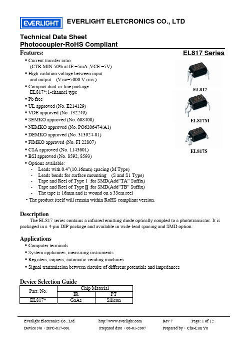
Photocoupler-RoHS Compliant EL817 SeriesFeatures: • Current transfer ratio(CTR:MIN.50% at IF =5mA ,VCE =5V) • High isolation voltage between input and output (Viso=5000 V rms ) • Compact dual-in-line package EL817*:1-channel type • Pb free• UL approved (No. E214129) • VDE approved (No. 132249) • SEMKO approved (No. 608400)• NEMKO approved (No. PO6206474/A1) • DEMKO approved (No. 313924-01)• FIMKO approved (No. FI 22807) • CSA approved (No. 1143601) • BSI approved (No. 8592, 8593) • Options available:- Leads with 0.4”(10.16mm) spacing (M Type)- Leads bends for surface mounting (S and S1 Type) - Tape and Reel of Type for SMD(Add”TA” Suffix)Ⅰ - Tape and Reel of Type Ⅱfor SMD(Add”TB” Suffix) - The tape is 16mm and is wound on a 33cm reel• The product itself will remain within RoHS compliant version.DescriptionThe EL817 series contains a infrared emitting diode optically coupled to a phototransistor. It is packaged in a 4-pin DIP package and available in wide-lead spacing and SMD option.Applications• Computer terminals• System appliances, measuring instruments• Registers, copiers, automatic vending machines• Signal transmission between circuits of different potentials and impedancesDevice Selection GuideChip MaterialPart. No.IR PTEL817* GaAs SiliconEL817EL817SEL817MPhotocoupler-RoHS CompliantEL817 SeriesPhotocoupler-RoHS CompliantEL817 SeriesS1 TypeNotes:1.Rank shall be or shall not be marked2.Factory code shall be marked (T: Taiwan / C: China)3.Year date code4.2-digit work week5.All dimensions are in millimeters6.Specifications are subject to change without noticePhotocoupler-RoHS Compliant EL817 SeriesAbsolute Maximum Ratings ( Ta=25°C )Parameter Symbol Rating UnitForward Current I F 50 mAPeak Forward Current*1I FM 1 A Input Reverse VoltageV R 6 V Power Dissipation P 70 mWCollector Power DissipationP C 150 mW Output Collector CurrentI C 50mA Collector-Emitter Voltage V CEO 35 V Emitter-Collector Voltage V ECO 6V Total Power DissipationPtot 200 mW *2Isolation Voltage Viso 5000 V rms Operating TemperatureTopr -55~+110 °C Storage TemperatureTstg -55~+125 °C *3Soldering TemperatureTsol260°C*1Frequency=100 HZ ,10uS Duty*2AC for 1 minute, R.H= 40~ 60%RH-Isolation voltage shall be measured using the following method. (1) Short between anode and cathode on the primary side and between collector, emitter and base on the secondary side.(2) The isolation voltage tester with zero-cross circuit shall be used. (3) The waveform of applied voltage shall be a sine wave*3For 10 secondsPhotocoupler-RoHS Compliant EL817 SeriesElectro-Optical Characteristics (Ta=25°C)Parameter Symbol Min. Typ. Max. Unit ConditionForward V F - 1.2 1.4 V I F =20mA Peak ForwardCurrent V FM 3.0 V I FM =0.5A Reverse Current I R - - 10 uAV R =4VInputTerminal Ct - 30 250 pF V=0,f=1kHz Collector Dark currentI CEO - - 100 nAV CE =20VOutputCollector- Emitter breakdown voltage BV CEO 35 - - V Ic=0.1mACurrent Transfer ratio CTR 50-600 % I F =5mA ,V CE =5VCollector- Emitter saturation voltageV CE(sat) - 0.1 0.2 V I F =20mA ,Ic=1 mAIsolation resistance R ISO 5×10¹⁰ 1011 - ΩDC500V,40~60%R.HFlotation capacitance Cf - 0.6 1.0 pF V=0, f=1MHz Cut-off frequency fc - 80 - kHz V CE =5V, I C =2 mAR L =100Ω, -3dBRise time t r - 4 18 us Transfer CharacteristicsFall timet f - 3 18 usV CE =2VI C =2mA,R L =100ΩPhotocoupler-RoHS CompliantEL817 Series SupplementCurrent Transfer Ratio CTRSub-Model No. Rank mark CTR (%) ConditionEL817* note 1 50 to 600EL817* (L) note2L 50 to 100EL817* (A) A 80 to 160EL817* (B) B 130 to 260 EL817* (C) C 200 to 400 EL817* (D) D 300 to 600 EL817* (AB) A or B 80 to 260 EL817* (BC) B or C 130 to 400 EL817* (CD) C or D 200 to 600 I F = 5 mA V CE = 5 V T a = 25°CNote1. The symbol “ * “ can be none or S or M by different leads form request Note2. The symbol “ ( ) ” can be CTR rankPhotocoupler-RoHS CompliantEL817 Series RELIABILITY PLANz The reliability of products shall be satisfied with items listed below.Confidence level : 90 % , LTPD : 10 %Classification Test Item Description & Condition (Acc.)Sample FailureCriteriaReferenceStandardOperation Life * Ta = 25±3°CIR: If = 50 mAPt: Pc = 130 mW ( Vf=1.4v) , 1000 hrs 0 / 22 MIL-S-750 : 1026MIL-S-883 : 1005JIS C 7021 : B-1High Temperature / High Humidity Reverse Bias (H3TRB) Ta = 85 ±3°C , Humi. = 85 % rhPt: 80% * Vce (max rating) , 1000 hrs0 / 22 JIS C 7021 : B-11High Temperature Reverse Bias (HTRB) Ta = 105 ±3°CPt: 100% * Vce (Max rating) ,1000 hrs0 / 22 JIS C 7021 : B-8Low Temperature Storage Ta = -50 ±3°C , 1000 hrs 0 / 22 JIS C 7021 : B-12High Temperature Storage Ta = 125 ±3°C , 1000 hrs 0 / 22 JIS C 7021 : B-10MIL-S-883 : 1008 Endurance testAuto clave P = 15 PSIG , Ta = 121 °C ,Humi. = 100 % rh , 48 hrs0 / 22 JESD 22-A102-BTemperature Cycling (Air to Air) 125°C ~ - 55 °C30 ~ 30 min , 100 cycles0 / 22 MIL-S-883 :1010JIS C 7021 : A-4Thermal Shock (Liquid to Liquid) 125 ~ - 55°Ct (dwell) = 5 mint (trans.) = 10 sec , 100 cycles0 / 22 MIL-S-202 : 107DMIL-S-750 : 1051MIL-S-883 :1011Solder Resistance Ta = 260 ±3°Ct (dwell) = 10 ±1 sec 0 / 22 MIL-S-750 : 2031JIS C 7021 : A-1Environmental TestSolder Ability Ta = 230 ±3 °Ct (dwell) = 5 ±1 sec 0 / 22CTR shift > 1.2Vf > U* 1.0Ir > U * 1.0Vce(sat) >U*1.0Bvceo < L*1.0Bveco < L*1.0L :LowSpec.LimitU : Up Spec.LimitMIL-S-883 : 2003JIS C 7021 : A-2Photocoupler-RoHS CompliantEL817 Seriesz Packing Quantity1.100 Pcs/ Per Tube2.25 Tubes / Inner Carton3.12 Inner Cartons / Outside Carton3. Outside Carton。
1 1206 Package Chip Infrared LED IR15-21C/TR8Features․Small double-end package ․High reliability․Low forward voltage․Good spectral matching to Si photodetector ․Pb free․The product itself will remain within RoHS compliant version. ․Compliance with EU REACHDescriptions․IR15-21C/TR8 is an infrared emitting diode in miniature SMD package which is molded in a water clear plastic With flat top view lens.․The device is spectrally matched with silicon photodiode and phototransistor.Applications․PCB mounted infrared sensor․Infrared emitting for miniature light barrier ․Floppy disk drive․Optoelectronic switch ․Smoke detector2Package DimensionsNotes: 1.All dimensions are in millimeters2.Tolerances unless dimensions ±0.1mm3.Suggested pad dimension is just for reference onlyPlease modify the pad dimension based on individual need3Notes: *1: Soldering time ≦5 seconds.45Typical Electro-Optical Characteristics Curves6 Precautions For Use1. Over-current-proofCustomer must apply resistors for protection, otherwise slight voltage shift will cause big current change (Burn out will happen). 2. Storage2.1 Do not open moisture proof bag before the products are ready to use.2.2 Before opening the package, the LEDs should be kept at 10℃~30℃ and 90%RH or less. 2.3 The LEDs suggested be used within one year.2.4 After opening the package, the devices must be stored at 10°C~30°C and 60%RH, and usedwithin 168 hours (floor life). If unused LEDs remain, it should be stored in moisture proof packages.2.5 If the moisture absorbent material (desiccant material) has faded or unopened bag hasexceeded the shelf life or devices (out of bag) have exceeded the floor life, baking treatment is required.2.6 If baking is required, refer to IPC/JEDEC J-STD-033 for bake procedure or recommend the following conditions:96 hours at 60°C ± 5°C and < 5 % RH (reeled/tubed/loose units) 3. Soldering Condition3.1 Pb-free solder temperature profile3.2 Reflow soldering should not be done more than two times. 3.3 When soldering, do not put stress on the LEDs during heating. 3.4 After soldering, do not warp the circuit board.7 4.Soldering IronEach terminal is to go to the tip of soldering iron temperature less than 350℃ for 3 seconds within once in less than the soldering iron capacity 25W. Leave two seconds and more intervals, and do soldering of each terminal. Be careful because the damage of the product is often started at the time of the hand solder. 5.RepairingRepair should not be done after the LEDs have been soldered. When repairing isunavoidable, a double-head soldering iron should be used (as below figure). It should be confirmed8Note : The tolerances unless mentioned are ±0.1mm, Unit: mm9 Label Form SpecificationCPN: Customer’s Production Number P/N : Production Number LOT No: Lot Number QTY: Packing Quantity HUE: Peak Wavelength CAT: RanksREF: Reference MSL-X: MSL LevelMade In: Manufacture placeNotes1. Above specification may be changed without notice. EVERLIGHT will reserve authority on material change for above specification.2. The graphs shown in this datasheet are representing typical data only and do not show guaranteed values.3. When using this product, please observe the absolute maximum ratings and the instructionsforuse outlined in these specification sheets. EVERLIGHT assumes no responsibility for any damage resulting from use of the product which does not comply with the absolute maximum ratings and the instructions included in these specification sheets.4. These specification sheets include materials protected under copyright of EVERLIGHT. Reproduction in any form is prohibited without the specific consent of EVERLIGHT.5. This product is not intended to be used for military, aircraft, automotive, medical, life sustaining or life saving applications or any other application which can result in human injury or death.Please contact authorized Everlight sales agent for special application request.。
Technical Data Sheet Chip Phototransistor With Right Angle LensPT12-21C/TR8Features․Fast response time ․High photo sensitivity ․Small junction capacitance ․Package in 8mm tape on 7” diameter reels. ․Pb free ․The product itself will remain within RoHS compliant version.Descriptions․PT12-21C/TR8 is a phototransistor in miniature SMD package which is molded in a water clear with right angle lens. The device is Spectrally matched to visible and infrared emitting diode.Applications․Miniature switch ․Counters and sorter ․Position sensor ․Infrared applied systemDevice Selection Guide LED Part No.PTChip MaterialSiliconLens ColorWater clearEverlight Electronics Co., Ltd. Device No:DTT-012-083http:\\ Prepared date:07-20-2005Rev 2Page: 1 of 10Prepared by:David Huang/PT12-21C/TR8Package DimensionsCollector EmitterNotes: 1.All dimensions are in millimeters 2.Tolerances unless dimensions ±0.1mmAbsolute Maximum Ratings (Ta=25℃)Parameter Collector-Emitter Voltage Emitter-Collector-Voltage Collector Current Operating Temperature Storage Temperature Soldering Temperature *1 Power Dissipation at(or below) 25℃Free Air Temperature Symbol VCEO VECO IC Topr Tstg Tsol Pc Rating 30 5 50 -25 ~ +85 -40 ~ +85 260 75 Units V V mA ℃ ℃ ℃ mWNotes: *1:Soldering time≦5 seconds.Everlight Electronics Co., Ltd. Device No:DTT-012-083http:\\ Prepared date:07-20-2005Rev 2Page: 2 of 10Prepared by:David Huang/PT12-21C/TR8Electro-Optical Characteristics (Ta=25℃)Parameter Rang Of Spectral Bandwidth Wavelength Of Peak Sensitivity Collector-Emitter Breakdown Voltage Emitter-Collector Breakdown Voltage Collector-Emitter Saturation Voltage Collector Dark Current Symbol λ0.5 λP BVCEO BVECO VCE(sat) ICEO Condition ----IC=100μA Ee=0mW/cm2 IE=100μA Ee=0mW/cm2 IC=2mA Ee=1m W/cm2 VCE=20V Ee=0mW/cm2 VCE=5V Ee=1mW /cm2 VCE=5V IC=1mA RL=1000Ω Min 400 --30 5 ----Typ --940 --------Max 1100 ------0.4 100 Unit nm nm V V V nAOn State Collector Current Rise Time Fall TimeIC(ON) tr tf0.3 -----1.14 15 15-----mAμS ---Everlight Electronics Co., Ltd. Device No:DTT-012-083http:\\ Prepared date:07-20-2005Rev 2Page: 3 of 10Prepared by:David Huang/PT12-21C/TR8Typical Electro-Optical Characteristics CurvesFig.1Collector Power Dissipation vs. Ambient Temperature Fig.2 Spectral Sensitivity100 80 60 40 20 01.0 Ta=25 C 0.8 0.6 0.4 0.2 0-250255075 85 100100 300 500 700 900 1100 1300Fig.3 Relative Collector Current vs. Ambient TemperatureFig.4 Collector Current vs. Irradiance160 140 120 100 80 60 40 20 0 0 10 20 30 40 50 60 702100 C 10 1 0.10.01 0.51325Everlight Electronics Co., Ltd. Device No:DTT-012-083http:\\ Prepared date:07-20-2005Rev 2Page: 4 of 10Prepared by:David Huang/PT12-21C/TR8Typical Electro-Optical Characteristics CurvesFig.5 Collector Dark Current vs. Ambient Temperature Fig.6 Collector Current vs. Collector-Emitter Voltage1014 1210 1010 8 610 10 0 25 50 75 1004 2 0 0 1 2 3 4Everlight Electronics Co., Ltd. Device No:DTT-012-083http:\\ Prepared date:07-20-2005Rev 2Page: 5 of 10Prepared by:David Huang/PT12-21C/TR8Precautions For Use1. Over-current-proof Customer must apply resistors for protection , otherwise slight voltage shift will cause big current change ( Burn out will happen ). 2. Storage 2.1 Do not open moisture proof bag before the products are ready to use. 2.2 Before opening the package, the LEDs should be kept at 30℃ or less and 90%RH or less. 2.3 The LEDs should be used within a year. 2.4 After opening the package, the LEDs should be kept at 30℃ or less and 70%RH or less. 2.5 The LEDs should be used within 168 hours (7 days) after opening the package. 2.6 If the moisture absorbent material (silica gel) has faded away or the LEDs have exceeded the storage time, baking treatment should be performed using the following conditions. Baking treatment : 60±5℃ for 24 hours. 3. Soldering Condition 3.1 Pb-free solder temperature profile3.2 Reflow soldering should not be done more than two times. 3.3 When soldering, do not put stress on the LEDs during heating. 3.4 After soldering, do not warp the circuit board.Everlight Electronics Co., Ltd. Device No:DTT-012-083http:\\ Prepared date:07-20-2005Rev 2Page: 6 of 10Prepared by:David Huang/PT12-21C/TR84.Soldering Iron Each terminal is to go to the tip of soldering iron temperature less than 280℃ for 3 seconds within once in less than the soldering iron capacity 25W. Leave two seconds and more intervals, and do soldering of each terminal. Be careful because the damage of the product is often started at the time of the hand solder. 5.Repairing Repair should not be done after the LEDs have been soldered. When repairing is unavoidable, a double-head soldering iron should be used (as below figure). It should be confirmed beforehand whether the characteristics of the LEDs will or will not be damaged by repairing.Everlight Electronics Co., Ltd. Device No:DTT-012-083http:\\ Prepared date:07-20-2005Rev 2Page: 7 of 10Prepared by:David Huang/PT12-21C/TR8Package DimensionsLoaded Quantity Per Reel 2000PCS/ReelCollector EmitterUnit : mmEverlight Electronics Co., Ltd. Device No:DTT-012-083http:\\ Prepared date:07-20-2005Rev 2Page: 8 of 10Prepared by:David Huang/PT12-21C/TR8Reliability Test Item And ConditionThe reliability of products shall be satisfied with items listed below. Confidence level:90% LTPD:10% NO. Item Test Conditions Test Hours/ Cycles 6Mins 50Cycles Sample Failure Sizes Judgement Criteria 22pcs 22pcs IC(ON)≦L×0.8 L:Lower 50Cycles 22pcs Specification Limit 0/1 Ac/Re1 REFLOW Soldering TEMP.:240℃±5℃ 5secs 15mins 2 Temperature Cycle H : +100℃ L : -40℃ 3 Thermal Shock H :+100℃ L :-10℃ 4 High Temperature Storage 5 Low Temperature Storage 5mins 15mins 5mins 10secs 5mins0/1 0/1TEMP.:+100℃ TEMP.:-40℃1000hrs 1000hrs 1000hrs 1000hrs22pcs 22pcs 22pcs 22pcs0/1 0/1 0/1 0/16 DC Operating Life VCE=5V 7 High Temperature/ 85℃ / 85% R.H High HumidityEverlight Electronics Co., Ltd. Device No:DTT-012-083http:\\ Prepared date:07-20-2005Rev 2Page: 9 of 10Prepared by:David Huang/PT12-21C/TR8Packing Quantity Specification1.2000Pcs/1Volume,1Volume/1Bag 2.10Boxes/1CartonLabel Form SpecificationCPN: Customer’s Production Number P/N : Production Number QTY: Packing Quantity CAT: Ranks HUE: Peak Wavelength REF: Reference LOT No: Lot Number MADE IN TAIWAN: Production PlaceRoHSPT12/21C/TR8Notes1. Above specification may be changed without notice. EVERLIGHT will reserve authority on material change for above specification. 2. When using this product, please observe the absolute maximum ratings and the instructions for using outlined in these specification sheets. EVERLIGHT assumes no responsibility for any damage resulting from use of the product which does not comply with the absolute maximum ratings and the instructions included in these specification sheets. 3. These specification sheets include materials protected under copyright of EVERLIGHT corporation. Please don’t reproduce or cause anyone to reproduce them without EVERLIGHT’s consent.EVERLIGHT ELECTRONICS CO., LTD. Office: No 25, Lane 76, Sec 3, Chung Yang Rd, Tucheng, Taipei 236, Taiwan, R.O.CTel: 886-2-2267-2000, 2267-9936 Fax: 886-2267-6244, 2267-6189, 2267-6306 http:\\Everlight Electronics Co., Ltd. Device No:DTT-012-083http:\\ Prepared date:07-20-2005Rev 2Page: 10 of 10Prepared by:David Huang/分销商库存信息: EVERLIGHTPT12-21C/TR8。
ir2117strpbf规格书【实用版】目录1.产品概述2.主要特性3.规格参数4.应用领域5.环境要求6.安全信息7.结构说明8.工作原理9.测试方法10.维护与保养正文1.产品概述ir2117strpbf 是一种高性能、低成本的电子元器件,具有出色的稳定性和可靠性。
它广泛应用于各种电子设备和系统中,为设备提供稳定的电源和信号传输功能。
2.主要特性ir2117strpbf 具有以下主要特性:- 高稳定性:在恶劣的工作环境下,仍能保持稳定的工作性能。
- 低失真:信号传输过程中失真度低,保证了信号的完整性和准确性。
- 宽工作温度范围:能在 -40℃至 +125℃的温度范围内正常工作。
- 抗干扰能力强:能有效抵抗各种电磁干扰,保证设备的正常运行。
3.规格参数ir2117strpbf 的规格参数如下:- 电压范围:3.3V-5V- 电流范围:50mA-100mA- 工作温度范围:-40℃至 +125℃- 存储温度范围:-40℃至 +125℃- 抗静电能力:±15KV- 封装形式:SOP-84.应用领域ir2117strpbf 广泛应用于以下领域:- 电子消费品:如电视机、收音机、音响设备等。
- 通讯设备:如手机、电话机、传真机等。
- 计算机及周边设备:如电脑、路由器、打印机等。
- 工业控制设备:如工控机、可编程控制器等。
5.环境要求为了保证 ir2117strpbf 的正常工作和延长使用寿命,应满足以下环境要求:- 避免阳光直射和潮湿环境。
- 避免暴露在高温、低温、高湿度的环境中。
- 避免与腐蚀性物质接触。
- 避免强烈的机械振动和冲击。
6.安全信息在操作和使用 ir2117strpbf 时,请注意以下安全信息:- 请勿用湿手触摸或操作设备。
- 请勿在未断电的情况下拆卸设备。
- 请确保设备接地良好,以防止静电损伤。
- 如有异常现象,请立即停止使用并联系专业人员处理。
7.结构说明ir2117strpbf 的结构说明如下:- 引脚 1:电源正极(VCC)- 引脚 2:电源负极(GND)- 引脚 3:输出信号(OUT)- 引脚 4:控制信号(CTRL)- 引脚 5:公共地(GND)- 引脚 6:公共地(GND)- 引脚 7:公共地(GND)- 引脚 8:输出信号(OUT)8.工作原理ir2117strpbf 的工作原理如下:当控制信号(CTRL)为高电平时,输出信号(OUT)跟随输入信号;当控制信号为低电平时,输出信号呈高阻态。
Technical Data Sheet 0805 Package Infrared Chip LEDIR17-21C/TR8Features․Small double-end package ․Low forward voltage ․Good spectral matching to Si photo detector ․Package in 8mm tape on 7” diameter reel ․Pb free ․The product itself will remain within RoHS compliant version.Descriptions․IR17-21C is an infrared emitting diode in miniature SMD package which is molded in a water clear plastic with flat top view lens. ․The device is spectrally matched with silicon photodiode and phototransistor.Applications․PCB mounted infrared sensor ․Infrared emitting for miniature light barrier ․Floppy disk drive ․Optoelectronic switch ․Smoke detectorDevice Selection GuideLED Part No. IR Chip Material GaAlAs Lens Color Water ClearEverlight Electronics Co., Ltd. Device No:DTR-017-041http:\\ Prepared date:07-20-2005Rev 2Page: 1 of 10Prepared by:Jaine Tsai芯天下--/IR17-21C/TR8Package DimensionsNotes: 1.All dimensions are in millimeters 2.Tolerances unless dimensions ±0.1mmAbsolute Maximum Ratings (Ta=25℃)Parameter Continuous Forward Current Peak Forward Current Reverse Voltage Operating Temperature Storage Temperature Soldering Temperature *2 Power Dissipation at(or below) 25℃Free Air Temperature *1 Symbol IF IFP VR Topr Tstg Tsol Pd Rating 65 1.0 5 -25 ~ +85 -40 ~ +85 260 130 Units mA A V ℃ ℃ ℃ mWNotes: *1:IFP Conditions--Pulse Width≦100μs and Duty≦1%. *2:Soldering time≦5 seconds.Everlight Electronics Co., Ltd. Device No:DTR-017-041http:\\ Prepared date:07-20-2005Rev 2Page: 2 of 10Prepared by:Jaine Tsai芯天下--/IR17-21C/TR8Electro-Optical Characteristics (Ta=25℃)Parameter Radiant Intensity Peak Wavelength Spectral Bandwidth Symbol Ee λp Δλ Condition IF=20mA IF=100mAPulse Width≦100μs ,Duty≦1%Min. 0.2 ---------Typ. 0.8 4.0 940 45 1.2 1.4 2.6 -120Max. ----1.5 1.8 4.0 10 --Units mW /sr nm nmIF=20mA IF=20mA IF=20mA IF=100mAPulse Width≦100μs ,Duty≦1%Forward VoltageVFVIF=1A Reverse Current View Angle IR 2θ1/2 VR=5V IF=20mAμA degEverlight Electronics Co., Ltd. Device No:DTR-017-041http:\\ Prepared date:07-20-2005Rev 2Page: 3 of 10Prepared by:Jaine Tsai芯天下--/IR17-21C/TR8Typical Electro-Optical Characteristics CurvesFig.1 Forward Current vs. Ambient Temperature140 120 100 80 60 40 200Fig.2 Spectral Distribution100 80 60 40 200 20 40 60 80 100IF=20mA Ta=25° C-250Fig.3 Peak Emission Wavelength Ambient Temperature980Fig.4 Forward Current vs. Forward Voltage4 109603 109409202 10900 -2502550751001 10 0 1 2 3 4Everlight Electronics Co., Ltd. Device No:DTR-017-041http:\\ Prepared date:07-20-2005Rev 2Page: 4 of 10Prepared by:Jaine Tsai芯天下--/IR17-21C/TR8Typical Electro-Optical Characteristics CurvesFig.5 Relative Intensity vs. Forward Current Fig.6 Relative Radiant Intensity vs. Angular Displacement100Ie-Radiant Intensity(mW/sr)-20-1001020 30101.0 0.940 50 60 70 80 0.6 0.4 0.2 0 0.2 0.4 0.610.8 0.7100010110210310 4IF-Forward Current (mA)Fig.7 Relative Intensity vs. Ambient Temperature(°C) Fig.8 Forward Voltage vs. Ambient Temperature(°C)1.01.30.8IF=20mA1.2IF=20mA0.61.10.425 50 75 100 120125 50 75 100 120Everlight Electronics Co., Ltd. Device No:DTR-017-041http:\\ Prepared date:07-20-2005Rev 2Page: 5 of 10Prepared by:Jaine Tsai芯天下--/IR17-21C/TR8Precautions For Use1. Over-current-proof Customer must apply resistors for protection , otherwise slight voltage shift will cause big current change ( Burn out will happen ). 2. Storage 2.1 Do not open moisture proof bag before the products are ready to use. 2.2 Before opening the package, the LEDs should be kept at 30℃ or less and 90%RH or less. 2.3 The LEDs should be used within a year. 2.4 After opening the package, the LEDs should be kept at 30℃ or less and 70%RH or less. 2.5 The LEDs should be used within 168 hours (7 days) after opening the package. 2.6 If the moisture absorbent material (silica gel) has faded away or the LEDs have exceeded the storage time, baking treatment should be performed using the following conditions. Baking treatment : 60±5℃ for 24 hours. 3. Soldering Condition 3.1 Pb-free solder temperature profile3.2 Reflow soldering should not be done more than two times. 3.3 When soldering, do not put stress on the LEDs during heating. 3.4 After soldering, do not warp the circuit board.Everlight Electronics Co., Ltd. Device No:DTR-017-041http:\\ Prepared date:07-20-2005Rev 2Page: 6 of 10Prepared by:Jaine Tsai芯天下--/IR17-21C/TR84.Soldering Iron Each terminal is to go to the tip of soldering iron temperature less than 280℃ for 3 seconds within once in less than the soldering iron capacity 25W. Leave two seconds and more intervals, and do soldering of each terminal. Be careful because the damage of the product is often started at the time of the hand solder. 5.Repairing Repair should not be done after the LEDs have been soldered. When repairing is unavoidable, a double-head soldering iron should be used (as below figure). It should be confirmed beforehand whether the characteristics of the LEDs will or will not be damaged by repairing.Everlight Electronics Co., Ltd. Device No:DTR-017-041http:\\ Prepared date:07-20-2005Rev 2Page: 7 of 10Prepared by:Jaine Tsai芯天下--/IR17-21C/TR8Reliability Test Item And Condition The reliability of products shall be satisfied with items listed below. Confidence level:90% LTPD:10% NO. Item Test Conditions Test Hours/ Sample Cycles Sizes 22pcs 22pcs IR≧U×2 Ee≦L×0.8 VF≧U×1.2 U:Upper Specification Limit L:Lower Specification Limit Failure Judgement Criteria Ac/Re1 REFLOW Soldering TEMP.:260℃±5℃ 6Mins 5secs 15mins 50Cycles 2 Temperature Cycle H : +100℃ 5mins L : -40℃ 15mins 3 Thermal Shock H :+100℃ L :-10℃ 4 High Temperature Storage 5 Low Temperature Storage 5mins 50Cycles 10secs 5mins 1000hrs 1000hrs 1000hrs 1000hrs0/1 0/122pcs0/1TEMP.:+100℃ TEMP.:-40℃22pcs 22pcs 22pcs 22pcs0/1 0/1 0/1 0/16 DC Operating Life IF=20mA 7 High Temperature/ 85℃ / 85% R.H High HumidityEverlight Electronics Co., Ltd. Device No:DTR-017-041http:\\ Prepared date:07-20-2005Rev 2Page: 8 of 10Prepared by:Jaine Tsai芯天下--/IR17-21C/TR8Package DimensionsTaping DimensionsUnit:mmEverlight Electronics Co., Ltd. Device No:DTR-017-041http:\\ Prepared date:07-20-2005Rev 2Page: 9 of 10Prepared by:Jaine Tsai芯天下--/IR17-21C/TR8Packing Quantity Specification1.3000Pcs/1Volume,1Volume/1Bag 2.10Boxes/1CartonLabel Form SpecificationCPN: Customer’s Production Number P/N : Production Number QTY: Packing Quantity CAT: Ranks HUE: Peak Wavelength REF: Reference LOT No: Lot Number MADE IN TAIWAN: Production PlaceRoHSIR17-21C/TR8Notes1. Above specification may be changed without notice. EVERLIGHT will reserve authority on material change for above specification. 2. When using this product, please observe the absolute maximum ratings and the instructions for using outlined in these specification sheets. EVERLIGHT assumes no responsibility for any damage resulting from use of the product which does not comply with the absolute maximum ratings and the instructions included in these specification sheets. 3. These specification sheets include materials protected under copyright of EVERLIGHT corporation. Please don’t reproduce or cause anyone to reproduce them without EVERLIGHT’s consent.EVERLIGHT ELECTRONICS CO., LTD. Office: No 25, Lane 76, Sec 3, Chung Yang Rd, Tucheng, Taipei 236, Taiwan, R.O.C Tel: 886-2-2267-2000, 2267-9936 Fax: 886-2267-6244, 2267-6189, 2267-6306 http:\\Everlight Electronics Co., Ltd. Device No:DTR-017-041http:\\ Prepared date:07-20-2005Rev 2Page: 10 of 10Prepared by:Jaine Tsai芯天下--/。