HOLTEK推出HT1632C 更Powerful的LED Driver
- 格式:doc
- 大小:1.13 KB
- 文档页数:1

HT32F12365/HT32F12366/HT32F22366产品规格书带Arm® Cortex®-M3内核以及1 MSPS ADC、USART、UART、SPI、I2C、I2S、MCTM、GPTM、BFTM、PDMA、SCI、CRC、RTC、WDT、AES、EBI、CSIF和USB 2.0 FS 高达256KB Flash和128KB SRAM的 Holtek 32-Bit单片机版本: V1.30 日期: 2020-09-16目录目录1 简介 (6)2 特性 (7)内核 (7)片上存储器 (7)Flash 存储器控制器 – FMC (7)复位控制单元 – RSTCU (7)时钟控制单元 – CKCU (8)电源管理 – PWRCU (8)外部中断/事件控制器 – EXTI (8)模数转换器 – ADC (8)模拟比较器 – CMP (9)I/O 端口 – GPIO (9)马达控制定时器 – MCTM (9)通用功能定时器 – GPTM (10)基本功能定时器 – BFTM (10)看门狗定时器 – WDT (10)实时时钟 – RTC ................................................................................................................................10内部集成电路 – I 2C . (11)串行外设接口 – SPI (11)通用同步异步收发器 – USART (11)通用异步收发器 – UART (12)智能卡接口 – SCI .............................................................................................................................12内置音频接口 – I 2S (12)循环冗余校验 – CRC (13)外设直接访问内存 – PDMA (13)外部总线接口 – EBI (13)通用串行总线设备控制器 – USB (14)高级加密标准– AES (14)安全数字输入/输出 – SDIO (14)CMOS 传感器接口 – CSIF (仅用于HT32F22366) (14)调试支持 (15)封装和工作温度 (15)3 概述 (16)单片机信息 (16)方框图 (17)目录存储器映射 (18)时钟结构 (21)4 引脚图 (22)5 电气特性 (32)极限参数 (32)建议直流特性 (32)片上LDO稳压器特性 (32)功耗 (33)复位和电源监控特性 (34)外部时钟特性 (35)内部时钟特性 (36)PLL特性 (36)USB PLL特性 (36)存储器特性 (37)I/O端口特性 (37)A/D转换器特性 (38)比较器特性 (39)GPTM/MCTM特性 (40)I2C特性 (41)SPI特性 (42)I2S特性 (44)SDIO特性 (45)CSIF特性 (46)USB特性 (47)6 封装信息 (48)SAW Type 46-pin QFN (6.5mm×4.5mm×0.75mm) 外形尺寸 (49)48-pin LQFP (7mm×7mm) 外形尺寸 (50)64-pin LQFP (7mm×7mm) 外形尺寸 (51)100-pin LQFP (14mm×14mm) 外形尺寸 (52)表列表表列表表1. 特性及外设列表 (16)表2. 寄存器映射 (19)表3. 46-pin QFN ,48/64/100-pin LQFP 封装引脚图 (26)表4. 引脚描述 (29)表5. 极限参数 (32)表6. 建议直流工作条件 (32)表7. LDO 特性 (32)表8. 功耗特性 ..........................................................................................................................................................33表9. V DD 电源复位特性 . (34)表10. LVD/BOD 特性 (34)表11. 外部高速时钟 (HSE) 特性 (35)表12. 外部低速时钟 (LSE) 特性 (35)表13. 内部高速时钟 (HSI) 特性 (36)表14. 内部低速时钟 (LSI) 特性 (36)表15. PLL 特性 (36)表16. USB PLL 特性 (36)表17. Flash 存储器特性 (37)表18. I/O 端口特性 (37)表19. A/D 转换器特性 (38)表20. 比较器特性 (39)表21. GPTM/MCTM 特性.......................................................................................................................................40表22. I 2C 特性 . (41)表23. SPI 特性 (42)图11. SPI 时序图 – SPI 从机模式,CPHA = 1 ......................................................................................................43表24. I 2S 特性 . (44)表25. SDIO 特性 (45)表26. USB 直流电气特性 (46)表27. USB 直流电气特性 (47)表28. USB 交流电气特性 (47)图列表图列表图1. 方框图 (17)图2. 存储器映射 (18)图3. 时钟结构图 (21)图4. 46-pin QFN引脚图 (22)图5. 48-pin LQFP引脚图 (23)图6. 64-pin LQFP引脚图 (24)图7. 100-pin LQFP引脚图 (25)图8. A/D转换器采样网络模板 (39)图9. I2C时序图 (41)图10. SPI时序图 – SPI主机模式 (43)图12. I2S主机模式时序图 (44)图13. I2S从机模式时序图 (45)图14. SDIO默认模式 (46)图15. SDIO高速模式 (46)图16. USB信号上升时间、下降时间和交叉点电压(V CRS)定义 (47)1 简介1 简介该系列的Holtek 单片机是一款基于Arm ®Cortex ®-M3处理器内核的32-bit 高性能低功耗单片机。

TM1642是一种带键盘扫描接口的恒流LED(发光二极管显示器)驱动控制专用电路,内部集成有MCU 数字接口、数据锁存器、LED 高压驱动、键盘扫描等电路。
本产品性能优良,质量可靠。
主要应用于段码LED产品的恒流显示屏驱动。
采用SOP28的封装形式。
功能特点•采用功率CMOS 工艺•多种显示模式(10段×7位~13段×4位)•SEG 恒流驱动最大电压值:VDD-1V •通道差最大+/-3%芯片间最大+/-6%•键扫描(8×2)•辉度调节电路(软件8级恒流可调)•串行接口(CLK,STB,DIN)•振荡方式:内置RC 振荡(450KHz+5%)•内置上电复位电路•封装形式:SOP28管脚信息123456789101112131415161718192021222324TM1642NCDINCLK STB K1K2VDDSEG1/KS1SEG2/KS2SEG3/KS3SEG4/KS4SEG5/KS5SEG6/KS6SEG7/KS7SEG8/KS8SEG9SEG10GRID1GRID2GRID3GRID4SEG14/GRID5SEG13/GRID SEG12/GRID VDD GND GND GND 25262728TOP VIEWSOP28深圳市富瑞世嘉科技有限公司13530167943天微专营为高时,CLK 被忽略输入该脚的数据在显示周期结束后被锁存段恒流输出(也用作键扫描),p管开漏输出16~17段恒流输出,P管开漏输出27、2624、23位输出,N管开漏输出输出(段/位)18~20段/位复用输出,只能选段或位输出逻辑电源7、215V±10%逻辑地22、25、28接系统地▲注意:DIN口输出数据时为N管开漏输出,在读键的时候需要外接1K-10K的上拉电阻,如图(1)所示。
本公司推荐10K的上拉电阻。
DOUT在时钟的下降沿控制N管的动作,此时读数不稳定,可以参考图(4),在时钟的上升沿时读数才稳定。
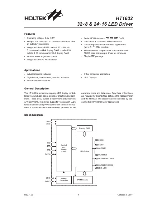
HT163232´8&24´16LED DriverBlock DiagramRev.1.001October 2,2007General DescriptionThe HT1632is a memory mapping LED display control-ler/driver,which can select a number of out bits and com-mons.These are 32out bits &8commons and 24out bits &16commons.The device supports 16-gradation LEDs for each out line using PWM control with software instruc-tions.A serial interface is conveniently provided for thecommand mode and data mode.Only three or four lines are required for the interface between the host controller and the HT1632.The display can be extended by cas-cading the HT1632for wider applications.Features·Operating voltage:2.4V~5.5V·Multiple LED display -32out bits/8commons and24out bits/16commons·Integrated display RAM -select 32out bits &8commons for 64´4display RAM,or select 24outbits &16commons for 96´4display RAM·16-level PWM brightness control ·Integrated 256kHz RC oscillator·Serial MCU interface -CS,RD,WR,DATA ·Data mode &command mode instruction ·Cascading function for extended applications(up to 5HT1632s possible)·Selectable NMOS open drain output driver andPMOS open drain output driver for commons·52-pin QFPpackageApplications·Industrial control indicator·Digital clock,thermometer,counter,voltmeter ·Instrumentation readouts·Other consumer application ·LED DisplaysPin AssignmentPin DescriptionPad Name I/O Description OUTBIT0~OUTBIT23O Line drivers.These pins drive the LEDs. OUTBIT24/COM15~OUTBIT31/COM8O Drive LED output or Common outputCOM0~COM7O Common outputsSYNC I/O Cascade synchronization input and outputOSC I/O If the system clock is is sourced from an external clock source,the external clock source should be connected to this pad.If the on-chip RC oscillator is selected, this pad can be connected to a high or low level.If the cascade mode is selected, this pad is the driver clock signal.DATA I/O Serial data input or output with pull-high resistorWR I WRITE clock input with pull-high resistor Data on the DATA lines are latched into the HT1632on the rising edge of the WR signal.RD I READ clock input with pull-high resistor.The HT1632RAM data is clocked out on the falling edge of the RD signal.The clocked out data will appear on the DATA line.The host controller can use the next rising edge to latch the clocked out data.CS I Chip select input with pull-high resistor When the CS line is high,the data and command read from or written to the HT1632is disabled,and the serial interface circuit is also reset.If CS is low,the data and command transmission between the host controller and the HT1632are all enabled.LED_VSS¾Negative power supply for driver circuit,ground.VSS¾Negative power supply for logic circuit,ground.VDD¾Positive power supply for logic and driver circuit.Rev.1.002October2,2007Absolute Maximum RatingsSupply Voltage...........................V SS-0.3V to V SS+5.5V Storage Temperature............................-50°C to125°C Input Voltage.............................V SS-0.3V to V DD+0.3V Operating Temperature...........................-40°C to85°CNote:These are stress ratings only.Stresses exceeding the range specified under²Absolute Maximum Ratings²may cause substantial damage to the device.Functional operation of this device at other conditions beyond those listed in the specification is not implied and prolonged exposure to extreme conditions may affect device reliability. D.C.Characteristics Ta=25°CSymbol ParameterTest ConditionsMin.Typ.Max.Unit V DD ConditionsV DD Operating Voltage¾¾ 2.45 5.5VI DD Operating Current5V No load,LED ON,on-chip RC oscillator¾¾10mAI STB Standby Current5V No load,power down mode¾¾10m AV IL Input Low Voltage5V DATA,WR,CS,RD0¾1VV IH Input High Voltage5V DATA,WR,CS,RD4¾5VI OL1DATA5V V OL=0.5V 1.3 2.6¾mAI OH1DATA5V V OH=4.5V-0.9-1.8¾mAI OL2OSC,SYNC5V V OL=0.5V 2.6 5.2¾mAI OH2OSC,SYNC5V V OH=4.5V-1.8-3.6¾mAI OL3Common Sink Current5V V OL=0.5V¾50¾mAI OH3Common Source Current5V V OH=4.5V¾-20¾mAI OL4LED Out Driver5V V OL=0.5V¾50¾mAR PH Pull-high Resistor5V DATA,WR,CS,RD103060k W Rev.1.003October2,2007A.C.CharacteristicsTa=25°C Symbol ParameterTest ConditionsMin.Typ.Max.Unit V DD Conditionsf SYS System Clock5V On-chip RC oscillator ¾256¾kHz f LED LED Duty Cycle &Frame Frequency5V 1/8duty ¾97.5¾Hz 5V 1/16duty ¾97.5¾Hz f CLK1Serial Data Clock (WR pin)5V Duty cycle 50%4¾300kHz f CLK2Serial Data Clock (RD pin)5VDuty cycle 50%¾¾150kHz t CS Serial Interface Reset Pulse Width¾CS 250¾¾ns t CLK WR,RD Input Pulse Width 5V Write mode 1.67¾¾m s Read mode3.34¾¾t r ,t f Rise/Fall Time Serial Data Clock Width (Figure 1)¾¾120¾¾ns t su Setup Time forDATA to WR,RD Clock Width (Figure 2)¾¾120¾¾ns t h Hold Time for DATA to WR,RD,Clock Width (Figure 2)¾¾120¾¾ns t su1Setup Time for CS to WR,RD,Clock Width (Figure 3)¾¾100¾¾ns t h1Hold Time for CS to WR,RD,Clock Width (Figure 3)¾¾100¾¾nsRev.1.004October 2,2007Figure 1Figure 2Figure 3Functional DescriptionDisplay Memory-RAMThe static display memory,RAM,is organised into64´4 bits or96´4bits and stores the displayed data.If32out bits&8commons is selected,the RAM size is64´4bits. If24out bits&16commons is selected the RAM size is 96´4bits.The contents of the RAM are directly mapped to the contents of the LED driver.Data in the RAM can be accessed by the READ,WRITE,and READ-MODIFY-WRITE commands.The following table shows the mapping from the RAM to the LED pattern:3Com2Com1Com0Addr.Out001H00H Out103H02H Out205H04H Out307H06H Out409H08H Out50BH0AH Out60DH0CH Out70FH0EH Out811H10H Out913H12H Out1015H14H Out1117H16H Out1219H18H Out131BH1AH Out141DH1CH Out151FH1EH Out1621H20H Out1723H22H Out1825H24H Out1927H26H Out2029H28H Out212BH2AH Out222DH2CH Out232FH2EH Out2431H30H Out2533H32H Out2635H34H Out2737H36H Out2839H38H Out293BH3AH Out303DH3CH Out313FH3EH D3D2D1D0Data D3D2D1D0Data32Outbits&8Common for64´4Display RAMRev.1.005October2,20073Com2Com1Com0Addr.Out003H.........00HOut107H04H Out20BH08H Out30FH0CH Out413H10H Out517H14H Out61BH18H Out71FH1CH Out823H20H Out927H24H Out102BH28H Out112FH2CH Out1233H30H Out1337H34H Out143BH38H Out153FH3CH Out1643H40H Out1747H44H Out184BH48H Out194FH4CH Out2053H50H Out2157H54H Out225BH58H Out235FH.........5CH D3D2D1D0Data D3D2D1D0Data24Outbits&16Common for96´4Display RAMRev.1.006October2,2007System OscillatorThe HT1632system clock is used to generate the time base clock frequency,LED-driving clock.The clock may be sourced from an on-chip RC oscillator(256kHz),or an external clock using the S/W setting.The configura-tion of the system oscillator is as shown.After the SYS DIS command is executed,the system clock will stop and the LED duty cycle generator will turn off.This com-mand is,however,available only for the on-chip RC os-cillator.Once the system clock stops,the LED display will become blank,and the time base will also lose its function.The LED OFF command is used to turn the LED duty cycle generator off.After the LED duty cycle generator switches off by issuing the LED OFF com-mand,using the SYS DIS command reduces power consumption,serving as a system power down com-mand.But if the external clock source is chosen as the system clock,using the SYS DIS command can neither turn the oscillator off nor execute the power down mode. The crystal oscillator option can be applied to connect an external frequency source to the OSC pin.In this case,the system fails to enter the power down mode, similar to the case in the external clock source opera-tion.At the initial system power on,the HT1632is in the SYS DIS state.LED DriverThe HT1632has a256(32´8)and384(24´16)pattern LED driver.It can be configured in a32´8or24´16pat-tern and common pad N-MOS open drain output or P-MOS open drain output LED driver using the S/W configuration.This feature makes the HT1632suitable for multiple LED applications.The LED-driving clock is derived from the system clock.The driving clock fre-quency is always256kHz,an on-chip RC oscillator fre-quency,or an external frequency.The LED corresponding commands are summarized in the table. The bold form of100,namely100,indicates the com-mand mode ID.If successive commands have been is-sued,the command mode ID except for the first command will be omitted.The LED OFF command turns the LED display off by disabling the LED duty cycle gen-erator.The LED ON command,on the other hand,turns the LED display on by enabling the LED duty cycle gen-erator.NameCommandCodeFunctionLED OFF10000000010X Turn off LED outputs LED ON10000000011X Turn on LED outputsCommonsOption1000010abXXXab=00:N-MOS opendrain output and8com-mon optionab=01:N-MOS opendrain output and16common optionab=10:P-MOS opendrain output and8com-mon optionab=11:P-MOS opendrain output and16common optionLED Color Current-limiting Resistor Red120WGreen100W Recommended Current-limiting Resistor for NMOSOpen Drain Driving ModeSystem Oscillator ConfigurationNMOS Open Drain Driving Mode ConfigurationPMOS Open Drain Driving Mode ConfigurationRev.1.007October2,2007BlinkerThe HT1632has display blinking capabilities.The blink function generates all LED blinking.The blink rates is 0.25ms LED on and0.25ms LED off for one blinking pe-riod.This blinking function can be effectively performed by setting the BLINK ON or BLINK OFF command.Command FormatThe S/W setting can configure the HT1632.There are two mode commands to configure the HT1632resources and to transfer the LED display data.The configuration mode of the HT1632is knows as the command mode,with a command mode ID of100.The command mode consists of a system configuration command,a system frequency selection command,a LED configura-tion command,and an operating command.The data mode,on the other hand,includes READ,WRITE,and READ-MODIFY-WRITE operations.The following are the data mode ID and the command mode ID:Operation Mode ID READ Data110 WRITE Data101 READ-MODIFY-WRITE Data101 COMMAND Command100The mode command should be issued before the data or command is transferred.If successive commands have been issued,the command mode ID,namely100, can be omitted.While the system is operating in the non-successive command or the non-successive ad-dress data mode,the pin should be set to²1²and the previous operation mode will be reset also.Once the CS pin returns to²0²,a new operation mode ID should be is-sued first.InterfacingOnly four lines are required to interface to the HT1632. The CS line is used to initialise the serial interface circuit and to terminate the communication between the host controller and the HT1632.If the CS pin is set to1,the data and command issued between the host controller and the HT1632are first disabled and then initialised. Before issuing a mode command or mode switching,a high level pulse is required to initialise the serial inter-face of the HT1632.The DATA line is the serial data in-put/output line.Data to be read or written or commands to be written have to be passed through the DATA line. The RD line is the READ clock input.Data in the RAM is clocked out on the falling edge of the RD signal,and the clocked out data will then appear on the DATA line.It is recommended that the host controller reads in the cor-rect data during the interval between the rising edge and the next falling edge of the RD signal.The WR line is the WRITE clock input.The data,address,and command on the DATA line are all clocked into the HT1632on the rising edge of the WR signal.Example of Waveform for BlinkerRev.1.008October2,2007Timing DiagramsREAD Mode-Command Code=110READ Mode-Successive Address ReadingWRITE Mode-Command Code=101WRITE Mode-Successive Address WritingRev.1.009October2,2007READ-MODIFY-WRITE Mode-Command Code=101READ-MODIFY-WRITE Mode-Successive Address AccessingCommand Mode-Command Code=100Mode-Data and Command ModeRev.1.0010October2,2007Application CircuitsSingle Connect Example for32Outbits&8CommonsNote:Common&outbit are all NMOS open drain output structures and only supply sink current.Rev.1.0011October2,2007Note:Outbit are NMOS open drain output structures and only supply sink current,common are PMOS open drain output structures and only supply source currentRev.1.0012October2,2007Note:It also can set cascade mode by er must set the Slaves in external clock mode with command.The CS pin must be connected to MCU individually for independent read-write.Rev.1.0013October2,2007Cascade Control FlowRev.1.0014October2,2007Command SummaryName ID Command Code D/C Function Def. READ110A6A5A4A3A2A1A0D0D1D2D3D Read data from the RAMWRITE101A6A5A4A3A2A1A0D0D1D2D3D Write data to the RAMREAD-MODIFY-WRITE101A6A5A4A3A2A1A0D0D1D2D3D Read and Write data to the RAMSYS DIS1000000-0000-X C Turn off both system oscillator and LED duty cycle generatorYesSYS EN1000000-0001-X C Turn on system oscillatorLED OFF1000000-0010-X C Turn off LED duty cycle generator Yes LED ON1000000-0011-X C Turn on LED duty cycle generatorBLINK OFF1000000-1000-X C Turn off blinking function Yes BLINK ON1000000-1001-X C Turn on blinking functionSLAVE MODE1000001-00XX-X Set slave mode and clock source from exter-nal clockMASTER MODE1000001-01XX-X Set master mode and clock source on-chip RC oscillator,the system clock output to OSC pinRC1000001-10XX-X C System clock source,on-chip RC oscillator Yes EXT CLK1000001-11XX-X C System clock source,external clock sourceCOMMONS OPTION 1000010-abXX-X Cab=00:N-MOS open drain output and8common optionab=01:N-MOS open drain output and16common optionab=10:P-MOS open drain output and8common optionab=11:P-MOS open drain output and16common optionab=10PWM Duty 100101X-0000-X C PWM1/16duty 100101X-0001-X C PWM2/16duty 100101X-0010-X C PWM3/16duty 100101X-0011-X C PWM4/16duty 100101X-0100-X C PWM5/16duty 100101X-0101-X C PWM6/16duty 100101X-0110-X C PWM7/16duty 100101X-0111-X C PWM8/16duty 100101X-1000-X C PWM9/16duty 100101X-1001-X C PWM10/16duty 100101X-1010-X C PWM11/16duty 100101X-1011-X C PWM12/16duty 100101X-1100-X C PWM13/16duty 100101X-1101-X C PWM14/16duty 100101X-1110-X C PWM15/16duty 100101X-1111-X C PWM16/16dutyRev.1.0015October2,2007Package Information52-pin QFP(14´14)Outline DimensionsSymbolDimensions in mmMin.Nom.Max.A17.3¾17.5B13.9¾14.1C17.3¾17.5D13.9¾14.1E¾1¾F¾0.4¾G 2.5¾ 3.1H¾¾ 3.4I¾0.1¾J0.73¾ 1.03K0.1¾0.2a0°¾7°Rev.1.0016October2,2007Holtek Semiconductor Inc.(Headquarters)No.3,Creation Rd.II,Science Park,Hsinchu,TaiwanTel:886-3-563-1999Fax:886-3-563-1189Holtek Semiconductor Inc.(Taipei Sales Office)4F-2,No.3-2,YuanQu St.,Nankang Software Park,Taipei115,TaiwanTel:886-2-2655-7070Fax:886-2-2655-7373Fax:886-2-2655-7383(International sales hotline)Holtek Semiconductor Inc.(Shanghai Sales Office)7th Floor,Building2,No.889,Yi Shan Rd.,Shanghai,China200233Tel:86-21-6485-5560Fax:86-21-6485-0313Holtek Semiconductor Inc.(Shenzhen Sales Office)5/F,Unit A,Productivity Building,Cross of Science M3rd Road and Gaoxin M2nd Road,Science Park,Nanshan District, Shenzhen,China518057Tel:86-755-8616-9908,86-755-8616-9308Fax:86-755-8616-9722Holtek Semiconductor Inc.(Beijing Sales Office)Suite1721,Jinyu Tower,A129West Xuan Wu Men Street,Xicheng District,Beijing,China100031Tel:86-10-6641-0030,86-10-6641-7751,86-10-6641-7752Fax:86-10-6641-0125Holtek Semiconductor Inc.(Chengdu Sales Office)709,Building3,Champagne Plaza,No.97Dongda Street,Chengdu,Sichuan,China610016Tel:86-28-6653-6590Fax:86-28-6653-6591Holtek Semiconductor(USA),Inc.(North America Sales Office)46729Fremont Blvd.,Fremont,CA94538Tel:1-510-252-9880Fax:1-510-252-9885CopyrightÓ2007by HOLTEK SEMICONDUCTOR INC.The information appearing in this Data Sheet is believed to be accurate at the time of publication.However,Holtek as-sumes no responsibility arising from the use of the specifications described.The applications mentioned herein are used solely for the purpose of illustration and Holtek makes no warranty or representation that such applications will be suitable without further modification,nor recommends the use of its products for application that may present a risk to human life due to malfunction or otherwise.Holtek¢s products are not authorized for use as critical components in life support devices or systems.Holtek reserves the right to alter its products without prior notification.For the most up-to-date information, please visit our web site at .Rev.1.0017October2,2007。

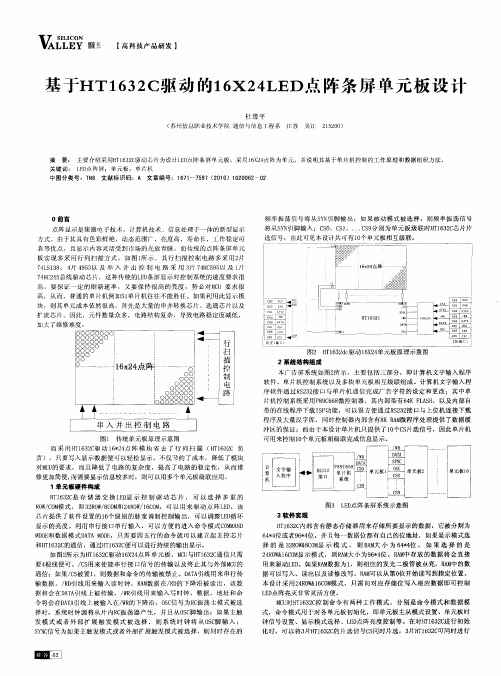
使用HT1632C 驱动点阵式LED 显示屏显示小绿人文件编码文件编码::HA0136S简介HT1632C 是一种Memory Mapping LED 显示驱动器,它广泛应用在数字时钟、温度计、湿度计等工业仪器仪表显示中。
步行小绿人Demo Board 是利用HT1632C 驱动由6个8×8LED 点阵块组成的24×16LED 点阵幕来显示小緑人行走动画。
采用HT48R10A-1为主芯片来控制HT1632C 进行数据传输,HT48R10A-1通过CS 、WR 、DATA 三根线将数据写入HT1632C 。
HT1632C 有两种显示方式:24 ROW/16 COM & 32 ROW/8 COM ,此设计采用24 ROW/16COM 显示方式。
步行小绿人由10幅不同姿势的画面来完成一个走路动作。
按键用来改变小绿人动作状态。
HT1632C 的基本特征• HT1632C 工作电压:2.4V~5.5V• 两种显示方式 (32 ROW & 8 COM 或24 ROW & 16 COM)• 内建显示RAM (若选32 ROW & 8 COM 显示方式,显示RAM 为64×4bit ;若选24 ROW & 16 COM 显示方式,显示RAM 为96×4bit) •16级PWM 亮度控制 •内建256K RC 振荡器 •与MCU 接口为串行接口方式 •与MCU 通讯有命令指令和数据指令 • Common 线可选为N-MOS Open drain 输出驱动或P-MOS Open drain 输出驱动硬件方块图ROW0~ROW23HT1632C图1主芯片为HT48R10A-1控制HT1632C LED Driver。
HT48R10A-1采用4M外部RC振荡,HT1632C采用内部150kHz RC Oscillator。
LED Driver的信号线CS、WR、DATA分别与HT48R10A-1的PA0、PA1、PA2相连接,主芯片HT48R10A-1一按键与PA.4相连。
HT1632C 在点阵式LED 显示屏中的应用 文件编码文件编码::HA0127S简介HT1632C 是一种Memory Mapping LED 显示驱动器,它广泛应用在数字时钟、温度计、湿度计等工业仪器仪表显示中,多片HT1632C CASCADE 的使用方法在点阵式LED 显示应用中尤为显著。
HT1632C 的基本特性如下:• HT1632C 工作电压:2.4V~5.5V• 多种显示方式(32 ROW & 8 COM 或24 ROW & 16 COM )• 内建显示RAM (若选32 ROW & 8 COM 显示方式,显示RAM 为64×4bit ;若选24 ROW & 16 COM 显示方式,显示RAM 为96×4bit )。
•16级PWM 亮度控制 •内建256K RC 振荡器 •与MCU 接口为串行接口方式 •与MCU 通讯有命令指令和数据指令 • COM 线可选为N-MOS Open Drain 输出驱动或P-MOS Open drain 输出驱动HT1632C 驱动LED 点数评估点阵式LED 显示屏结构最小的LED 点阵板我们现在要用HT1632C驱动的LED显示屏是用18块如上图所示的LED点阵板组成的144×8的点阵屏幕,效果图如下:HT1632C芯片选取评估上面已经介绍了一片HT1632C有32×8或24×16两种显示方式,我们现在要推动144×8点LED显示屏,HT1632C应选24×16显示方式,这样可驱动的LED点数较多。
(144×8)/(24×16)=3,这样用3片HT1632C就可完成以上LED显示屏的驱动。
单片HT1632C可驱动24×16=384点LED,一块LED点阵板有64点,那么一片HT1632C则可驱动6块最小的LED点阵板。
tm1638驱动共阳数码管原理TM1638驱动共阳数码管是一种常见的数码管驱动方案。
在解释TM1638驱动共阳数码管的原理之前,我们先来了解什么是共阳数码管,以及TM1638是什么。
共阳数码管是一种常见的数码管类型,它由多个发光二极管(LED)组成,每个LED代表一个数字或字母。
共阳数码管通过共阳极(anode)进行驱动,在驱动时将对应的共阳极引脚接高电平(一般为Vcc),通过控制各个阴极(cathode)引脚的低电平(接地),来控制每个LED是否发光。
而TM1638则是一种专门用于驱动共阳数码管的芯片。
它是一种集成了控制逻辑、译码器、数据存储器和其他功能的数字驱动器。
TM1638芯片通过与微控制器进行通信,实现对共阳数码管的控制。
TM1638驱动共阳数码管的原理主要分为以下几个步骤:1.初始化:通过与微控制器通信,将TM1638芯片初始化为特定的驱动模式,以便与共阳数码管进行正确的配合。
2.设置显示内容:通过微控制器发送数据给TM1638芯片,来设置共阳数码管的显示内容。
数据可以是数字、字母、符号等,通过数据存储器和译码器来将发送的数据转换为对应的控制信号。
3.扫描刷新:TM1638芯片通过控制共阳极的引脚来进行扫描刷新操作。
它会按照一定的时间间隔以及顺序依次点亮每个共阳数码管的LED,从而实现多位共阳数码管的显示。
4.控制亮度:TM1638芯片还可以通过调整引脚的PWM信号来控制共阳数码管的亮度。
总的来说,TM1638驱动共阳数码管的原理是通过与微控制器进行通信,将要显示的数据发送给TM1638芯片,然后通过控制共阳极和引脚的状态来实现数码管的驱动和显示。
TM1638驱动共阳数码管在实际应用中具有一些优点。
首先,TM1638芯片集成了多个控制和驱动功能,简化了电路设计和布局。
其次,它支持兼容SPI和I2C两种通信接口,方便与各种微控制器进行连接。
再次,TM1638芯片提供了多种控制功能,比如可以设置亮度、自动扫描等,提高了用户对数码管显示的控制能力。
holtek单片机图文全面详解电子产品项目中对单片机的选型,可谓仁者见仁智者见智。
合泰单片机价格适中,种类也比较齐全。
下面就为大家全面介绍下holtek的单片机。
holtek单片机是由盛群半导体设计开发,盛群半导体为国内专业微控制器IC设计领导厂商,营业范围主要包括微控制器IC及其周边组件之设计、研发与销售。
自1998年成立以来,公司不断致力于新产品的研发及技术的创新,加上对市场趋势的掌握,期能提供广大电子市场最具竞争力之IC产品。
产品范围包括:泛用型与专用型微控制器(MCU),除一般应用领域外,更涵盖语音、通讯、计算机外设、家电、医疗、车用及安全监控等各专业领域,并提供各种电源管理及非易失性内存等微控制器外围组件,提供客户更具竞争能力的完整解决方案。
holtek单片机分类(1)HT48系列I/O 型(+ LCD)(2)HT49系列I/O + LCD 型(3)HT46系列I/O+AD 型(+ LCD)(4)HT47系列I/O+RC-F(AD)+LCD+IR型(5)HT48xAx\HT49xAx系列Remote (遙控器用)型(6)HT95R2x\HT95R3x系列Phone(+ LCD)(7)HT45R3x\BS28xx\BS26xx系列Touch型(8)Flash 型(HT46Fxx\HT48Fxx\HT66Fxx\HT68Fxx)(9)TIny Power 型(HT56R2x,HT56R6x,HT56R6xx )(10)Keyboard/Mouse系列,USB Audio系列,V oice/Music系列,VFD系列。
HOLTEK单片机系统结构Holtek单片机的系统结构时序和流水线结构。
HOLTEK推出HT1632C 更Powerful的LED Driver
HOLTEK的LED Driver针对可直推LED应用而推出了HT1632C。
HT1632C是HT1632的特性增益版,在驱动能力、IC耗电、显示均匀度等都大幅提升特性,更适合直推LED。
HT1632C 尤其适用于健身器材、电子飞镖、万年历、信息显示及数字时钟等产品的应用。
HT1632C 延续HT1632的规格:工作电压工作电压2.4V~5.5V,可驱动2种分辨率的LED面板(32x8点及24x16点);具有16阶PWM亮度调节亮度调节功能;内建256kHz RC振荡器;可串接多组LED、扩大显示点数;内含Display RAM及支持MCU的串行接口方式接口方式。
HT1632C 系统工作频率工作频率除内建256kHz RC震荡频率外,并允许以外部时钟当成系统的工作频率,增加系统弹性。
HT1632C驱动电流加大至250mA,产品应用时可直推LED,不需外挂晶体管,减少生产成本生产成本。
HT1632C的单一整合Segment及Common的方案,让用户更容易控制显示画面及减少MCU I/O 口的使用,并可减少外围硬件线路及零件,大大节省客户使用IC的数量及成本。