Model Reduction for Power Electronics Systems with Multiple Heat Sources
- 格式:pdf
- 大小:148.81 KB
- 文档页数:5

1 West Coast Magnetics Advancing Power ElectronicsFOIL WINDINGS FOR SMPS INDUCTORS AND TRANSFORMERS Weyman Lundquist, CEO and Engineering Manager2•Solid wire⏹Litz wire⏹FoilTYPES OF WINDINGSLowest costLow DC resistance High AC winding lossEasy to wind Highest costHigher DC resistancePotential for low AC winding lossPractical limitation of 500 kHz due to lossInexpensiveVery Low DC resistancePotential for low AC winding loss3proximityskin dc rmsac dc dctotal P P R IR I P +++=2,22,rmsac ac ac IP R =dcdcdc R I P 2=Resistive lossEddy-currentlossdc lossac lossacrmsac ac R IP 2,=“ac resistance”WINDING LOSS COMPONENTS4PROXIMITY EFFECTJxOriginal drawing from SnellingB-Fieldxxx xxx xxx xxxx oo ooo ooo ooo ooCurrent DensityInduced CurrentMain Current⏹Proximity Effect⏹An isolated conductor is placed in an uniform external field ⏹External field results from other wires and windings near the conductor (transformer) and from the field present in the core winding window (inductor)PROXIMITY EFFECT55TransformerInductor Conductor Complexity Core gap Wave form Dowell yes yes Solid wire, foil 1 D No Sinusoidal Litz opt yes no Litz 2D Yes Sinusoidal Shape Opt no yes Litz 2D Yes Any Transformer Inductor Conductor Complexity Core gap Wave form Dowell Yes yes Solid wire, foil 1 D No Sinusoidal Litz opt Yes No Litz 2D Yes Sinusoidal Shape Opt No Yes Litz 2D Yes Any AnsysYesYesAll2D 3DYesYes•Design and Test Verification•Measure DCR (high accuracy)•Thermal measurement under load•Measure ESR (good for comparison of different windings, includes core loss induced by LCR meter)•Isolate winding loss using Network Analyzer *•Simulation Software* C.R. Sullivan, “A Step by Step Guide to Extracting Winding Resistance from an Impedance Measurement”, IEEE Apec 20176•Strategies for Loss Minimization in Foil Windings6Optimize foil thickness Minimize number of layersShape foil to take advantage of core geometry effects (WCM, Dartmouth Patent)Use multiple parallel foils and swap layersUse different foil thicknesses for different turns.Use a parallel litz or thin foil winding in the vicinity of a gap Interleave winding (transformers only)Use a low permeability material for core legSTUDYOPTIMIZATIONDesign and Test Verification:Model litz options: Litz optTest ESR from 100 kHz to 500 kHz to comparefoil and litz.Choose lowest loss option.Litz opt result:48 awg litz is lowest loss option.46 awg litz chosen due to cost.100 kHz: optimal number of strands: 3210500 kHz: optional number of strands: 871Choose 2700 strands, single layer, position asindicated in cross sectional view.9TRANSFORMER WINDING LOSS –CASE STUDY10RESULTS –TRANSFORMER10 DESIGNLitz is lowest loss optionTransformer constructed with 2700/46.Leakage L not sufficiently high.Bench testing indicates acceptable performance with room for loss reduction. NEXT STEPUse leakage layer to reduce space between windings, increase leakage L, and reduce loss. Investigate lower capacitance foil winding.1111INDUCTOR WINDING LOSS –CASE STUDY Inductance: 700 nHDC Current: 10 ampsRipple: 23 AppFrequency: 500 kHzDesign: 4 turns on EP13, gap of 1 mmSolution: Shape opt optimization, test ESR and DCR to estimate lossCompare to full foil and shaped foil.Shaped foil/cutout foil patent issued and second patent pendingWCM and DartmouthInductor Window Cross Section –Center Leg Gap12 Field Lines: Shape Opt Foil Cutout Cross Section Wire Placement: ShapeoptESR vs. Frequency Measurement 700 nH Inductor13Cutout: patent pendingInductor Total Winding Loss Including DC15Ripple magnitude above which litz has lower loss than copper foil for a 4 turn boost inductor100 kHz 63%6300200 kHz 37% 7400300 kHz 26%7800400 kHz 23% 9200500 kHz 20% 100001 MHz 18% 180002 MHz 15% 30000FrequencyPercent ProductWCM Shaped16 Foil InductorsLow loss gapped ferrite core, shaped foilwinding.Patent pending: Dartmouthand WCM17 Comparison of 10 uH, 55amp inductorsShaped Foil IronNickelToroidHighIronToroidHelicalCoilBased on 2015 WCM study, copies availableWinding Loss: Gapped Ferrite18 Cutout Patent issued: Dartmouth and WCMCONCLUSIONS19 Cut out foil for gapped inductor designs is the lowest loss option for inductors with DC current upto a ripple frequency product of about 7000. (% ripple * kHz)Both foil and litz are usable for inductors at frequencies up to 2 MHz as long as the ripple is lessthan 20%.Litz is very expensive with the cost increasing exponentially with frequency. In the cases noted inthe presentation the litz wire cost was 60% to 70% of the total material cost.For transformers, many high power applications require more turns, making foil windingoptimization critical.For gapped inductors shaped cutout foil has lower loss than full width foil, provided copper crosssection is the same.Future work to further examine effect of foil thickness as well as methods of reducing windingcapacitance in foil windings to extend performance to higher ripple and frequency values andto windings with more layers.Shaped foil/cutout foil patent issued and second patent pending WCM and Dartmouth20Thank you.。

电工翻译词汇M2micrometer,测微器micrometer checker,千分表检查仪microphone,传声器microphone calibration apparatus,传声器械校准仪microphone protection grid,传声器保护罩microphone response frequency,传声器共振频率microphone stand,传声器架microphone temperature coefficient,传声器温度系数microphotometer,测微光度计micropluviometer,微雨量器microtome,超薄切片机microwave,微波microwave detecton apparatus,微波检测仪microwave distance method,微波探伤法microwave distance meter,微波测距仪microwave hygroscope,微波测湿仪91microwave plasma detector,微波等离子体检测器microwave radar,微波雷达microwave radiometer,微波辐射计microwave remote sensing,微波遥感micro-wave scatterometer,微波散射计microwave thickness meter,微波厚度计mid infrared range(MIR) remote sensing,中红外遥感minimum achievable residual unbalance,最小可达剩余不平衡量minimum cyclic load,最小循环应力minimum detectable leak,最小可检漏量minimum detectable partial pressure,最小可检分压强minimum flow-rate,最小流量minmum load of the testing machine,试验机最小负荷minimum operationg pressure differential,最小工作压差minimum phase system,最小相位系统minimum positioning time,最小定位时间minimum power supply voltage,最低电源电压minimum rate of benefit,最低收益率minimum reserve,最低储备iminmum risk estimation,最小风险估计minimum scale value,标度始点值minimum strain,最小应变minimum temperature,最低温度minimum thermometer,最低温度计;最低温度表minimum variance estimation,最小方差估计mining compass,矿山罗盘仪mirror dial,镜大幅度盘mirror telescope,反射望远镜mixing length,混合长度mixing ratio,混合比mobile phase,流动相mobile weather station,流动气象站mobile X-ray detection apparatus,移动式X 射探伤机modal aggregation,模态集结modal control,模态控制modal matrix,模态矩阵modal transformation,模态变换mode of vibration,振型;振动模态mode shape,振形model,模型;型号model accuracy,模型精确度model analysis,模型分析model base(MB),模型库model base management system(MBMS),模型库管理系统92model checking,模型置信度model coordination method,模型协调法model decomposition,模型分解model design,模型设计model evaluation,模型评价model experiment,模型实验model fidelity,模型逼真度model following control system,模型跟踪控制系统model following controller,模型跟踪控制器model loading,模型装载model modification,模型修改model of strain gauge,应变计[片]型式model reduction,模型降价model reduction method,模型降价法model reference adaptive control system,模型参考适应控制系统model reference control system,模型参考控制系统model simplification,模型简化model transformation,模型变换model validation,模型确认model variable,模型变量model verification,模型验证modeling,建模modern control theory,现代控制理论modern polarography,近代极谱法modifiability,可修改性modular programming,模块化程序设计modularity,组合性modularization,模块化modulation,调制modulation analysis,调制分析modulation sideband,调制边带modulator,调制器modulator-demodulator;modem,调制解调器module,模块modulus of elasticity,弹性模量moire fringe,莫尔条纹moire frenge grating,莫尔条纹光栅moisture content,含湿量;水汽含量moisture sensor,湿敏元件molecular absorption spectrometry,分子吸收光谱法molecular beam mass spectrometer,调制分子束质谱计molecular spectrum,分子光谱molecule ion,分子离子moment,分矩93moment of pendulum,摆锤力矩monitoring,监视monitoring hardware,监视硬件monitoring program,监督程序monochromatic radiation,单色辐射monochromator,单色仪monocolour radiation,单色辐射monopole mass spectrometer,单极质谱计most economic control(MEC),最经济控制most economic observing(MEO),最经济观测mould growth test,长霉试验。

These symbols are intended to alert theuser to the presence of important operatingand maintenance instructions in the manualaccompanying the appliance.NOTICEUsing any part other than genuine Holman factory supplied parts relieves the manufacturer of all liability.Holman reserves the right to change specifications and product design without notice. Such revisions do not entitle the buyer to corresponding changes, improvements, additions or replacements for previously purchased equipment.Due to periodic changes in designs, methods, procedures, policies and regulations, the specifications contained in this sheet are subject to change without notice. While Holman Manufacturing exercises good faith efforts to provide information that is accurate, we are not responsible for errors or omissions in information provided or conclusions reached as a result of using the specifications. By using the information provided, the user assumes all risks in connection with such use.GENERAL SAFETY INFORMATIONThis equipment is designed and sold for commercial use only by personnel trained and experienced in its operation and is not sold for consumer use in and around the home nor for use directly by the general public in food service locations.Before using your new equipment, read and understand all the instructions & labels associated with the unit prior to putting it into operation. Make sure all people associated with its use understand the units operation & safety before they use the unit.All shipping containers should be checked for freight damage both visible and concealed. This unit has been tested and carefully packaged to insure delivery of your unit in perfect condition. If equipment is received in damaged condition, either apparent or concealed, a claim must be made with the delivering carrier. Concealed damage or loss - if damage or loss is not apparent until after equipment is unpacked, a request for inspection of concealed damage must be made with carrier within 15 days. Be certain to retain all contents plus external and internal packaging materials for inspection. The carrier will make an inspection and will supply necessary claim forms.GENERAL INSTALLATION INFORMATIONThe unit was shipped fully assembled and ready to plug into a standard outlet specified for its voltage and amp draw. If improper electrical supply is determined, contact a qualified electrician prior to using the unit. Removal and replacement of the power cord and plug will void the warranty. For assistance, contact your local authorized service agent for service or required maintenance. Level unit using the adjustable feet under the unit (approximately 1/2" adjustment).Before using the unit for the first time, wipe down the exterior with a damp cloth.Allow enough space around the toaster for adequate ventilation. Do not operate the unit without the crumb tray properly positioned. Overheating and poor toasting may occur. Read all labels on the unit and follow their instructions.MAINTENANCE AND REPAIRSContact the factory, a service representative or a local service company for service or required maintenance. Go to /scripts/manuals.aspx to find a service agent near you. Replacement cord sets must be purchased from Star Manufacturing International, Inc. or our authorized agents. Should you need any assistance regarding the operation or maintenance of any Holman equipment; write, phone, fax or e-mail our service department. In all correspondence mention the model number and the serial number of your unit, along with the voltage.Business Hours: 8 am to 4:30 p.m. Central Standard Time Telephone:(877) 242-0270Fax:(314) 781-2714E-mail:***********************************************************Website: Mailing Address: Star International Holdings Inc., Company10 Sunnen DriveSt. Louis, MO 63143U.S.A.MODELIRCS2-SBKConveyor ToastersElectronic ControlsIL27072M-Z17824, Rev. A 12/19/2013 CAUTIONELECTRICAL CONNECTIONBefore making any electrical connection to this unit, check that the power supply is adequate for the voltage, amperage and requirements stated on the rating plate. A wiring diagram is included in the Installation & Operations manual, which can be downloaded at /scripts/manuals.aspx .Disconnect the unit from the power source before installing or removing any parts.Be absolutely sure that the ground connection for the receptacle is properly wired. Do not connect equipment to power without proper ground connections. Improper grounding may result in personal injury or fatality.DO NOT CUT OR REMOVE THIS PLUG OR GROUNDING PRONG FROM THE PLUG.CONNECT/PLUG UNIT INTO DEDICATED A.C. LINE ONLY SPECIFIED ON THE DATAPLATE OF THE UNIT.CERTAIN SURFACES ARE EXTREMELY HOT DURING OPERATION AND CARE SHOULDBE TAKEN WHILE USING THIS UNIT.DO NOT IMMERSE OR LET THE UNIT STANDIN WATER.DO NOT HOSE DOWN THE UNIT OR THE TABLE/COUNTER IF THE UNIT IS ON THETABLE/COUNTER.KEEP AWAY FROM RUNNING WATER.INSTALLATION REQUIREMENTS1. Space: 16”x24”x18” (width x depth x height) inSpecialty Board of Breakfast Toaster Cart2. Electricity: 208/240 Volts, 30 Amps, NEMA L6-30RRecepticaleNOTE: Ensure to clean the toaster properly before using it for the first time. Refer to the Cleaning Procedure document for cleaning instructions.CAUTION WARNINGThe Holman IRCS conveyor toaster comes with pre-programmed factory default settings for CROISSANT, MUFFIN .Factory default settings are as follow:POWER SAVER SWITCHThere are three Power Saver modes:ON: Unit is in pre-programmed power saving setting.OFF: Power Saver mode is turned off.AUTO ON: Power Saver turns on when there has been no activityfor a programmed length of time.The operator may adjust the level of power reduction for the saver mode. (Note: conveyor may move slowly when in saver mode.)Two buttons (+) and (-) are used when increasing or decreasing the value of each programmable setting.A red LED light located at the lower portion of the control panel label will indicate if the value for top heat, bottom heat or conveyor speed is being adjusted.NEMA L6-30RWARNING WARNING WARNINGWARNINGCERTAIN SURFACES ARE EXTREMELY HOTDURING OPERATION AND CARE SHOULD BE TAKEN WHILE USING THIS UNIT.START UPWhen the toaster has been plugged into a suitable outlet and power supply, the word OFF will be displayed on the L.E.D. read out.A. Press the ON/OFF button once to turn on the toaster. The toaster will now enter into pre-heat and “PREHT” will be displayed (the elements will begin to glow but the conveyor and fan motor will not turn on).B. After one minute, the fan motor will turn on and the conveyor will begin turning at the previously saved setting (for initial start up, the drive motor will operate at the factory default setting).C. After 24 minutes, the display will show the last used programselection i.e. (for initial startup, CROIS, MUFFIN, will be the last program selected).DAILY OPERATIONCheck the power cord to insure that it is plugged into a proper outlet.Press the ON/OFF button once to turn the toaster on. Press the button a second time to turn the toaster off.NOTE: When the toaster is turned off, the fan and conveyor motors will continue to run for five minutes. The words COOL and DOWN will be alternately displayed during that time. After five minutes, the word OFF will be displayed until the ON/OFF button is pressed again.Once the toaster has been pre-heated, the menu buttons can be pressed to change to CROIS, MUFFIN, T3, T4.Menu buttons T5 & T6 are cheese melting features, when these buttons are pressed, the conveyor will stop and the display will count down. When finished, the conveyor will reverse for 10 seconds.OPERATING HINTS AND SAFETYIMPORTANT: If “HIGH TEMP” shows on the display1. Turn off the toaster and allow it to fully cool down.2. Inspect the fan inlet on the bottom of the toasterand remove anyting blocking the cooling fan inlet.3. Press the red high temperaure limit reset button onthe back of the toaster. (Note: There is one reset on each side). (Note: the toaster must be fully cool in order for the limit switch to reset).4. Turn on the toaster and check for proper operation.5. If cleaning the cooling fan inlet does not correctthe problem, contact the factory or an authorized service agency for required maintenance.Disconnect power to the unit with the ON/OFF button at the end of each day of operation.Do not leave the unit in operation without an attendant.Do not leave the unit at high temperature when not in use or during idle periods. This will cause food particles and grease film to carbonize.The cooling fan will continue to run until the toaster has completely cooled. If the toaster MUST be moved after using, allow the cooling fan to turn OFF before unplugging.CAUTION PROGRAMMING A. CONVEYOR SPEED (temporary setting)The conveyor speed is programmable with a range from 1 to 99 with1 being the slowest and 99 being the fastest. Each menu item can have independent conveyor speed settings.B. PROGRAMMING VALUES FOR MENU ITEMSTo make a program change to the top & bottom elements, or conveyor speed, you must first be in the menu item you want changed. Example: to change the programmed conveyor speed for croissants, the display must read CROIS . To change the programmed conveyorspeed for MUFFIN, the display must read MUFFIN and so on foreach menu item.1) Select the menu item you want to change i.e. CROIS, MUFFIN, T3, T4. 2) Press and hold both ( + ) AND ( - ) buttons for 3 seconds untilthe display goes blank, release the buttons and the display will show three characters for the menu item elected and the last two characters for the current value setting, i.e. CROIS, MUFFIN, T3, T4. The red L.E.D. light for upper front element at the bottom of the label will flash.3) Press the ( + ) or ( - ) buttons to increase or decrease thesetting for the upper element.4) Press the button for the menu button again and the red L.E.D.for the up lower element will flash.5) Press the ( + ) or ( - ) buttons to increase or decrease thesetting for the lower element. 6) Press the button for the menu button again and the red L.E.D.for the conveyor speed will flash.7) Press the ( + ) or ( - ) buttons to increase or decrease thesetting for the conveyor speed.8) Button T5 & T6 are cheese melting functions program. Theseare the same as above, but set a cheese melting time in seconds instead of conveyor speed.9) To skip one feature setting with out making any changes,press the menu item button one time and the red L.E.D. light for the next item will now flash.10) To change the POWER SAVER values press the SAVERbutton or to save your new setting(s), and exit the program mode press the menu button.11) The last two characters in the display will show MN forminutes.12) The first three characters will be numerical to represent thetime setting.13) When set to “OFF” the Saver button will be disabled duringoperation. The PowerSaver can be set to “OFF” or using the ( + ) or ( - ) set the time from 15 to 480 minutes.14) Press the SAVER button to change the power reduction usingthe ( + ) or ( - ) buttons to increase or decrease the setting.15) Press the POWER SAVER button to save changes and toexit.CLEANINGPreventive maintenance for your Holman toaster consists of the following recommended cleaning procedures. To keep your toaster in its top operating condition, these steps should be performed on a daily or weekly basis as required.SuppliesKAY® QSR Oven CleanerKAY® QSR Heavy Duty Multi-Purpose Sink Detergent (dispensed use solution)KAY® Sink Sanitizer (use solution prepared at the sink)No Scratch Pad Red ClothDaily Procedure:1. Turn toaster off, conveyor will continue to run until cooleddown (approx. 5-10 minutes)2. Immediately spray the oven cleaner onto the No ScratchPad and scrub the conveyor chain while it is still warm and moving.NOTE: DO NOT SPRAY directly onto the conveyor belt or into the cooking chamber. Overspray onto the heating elements can damage or shorten the life of the elements.3. Wash the No Scratch pad at the 3 compartment sink and thensoak with Multi-Purpose Sink Detergent. Ring the pad out so that it is only damp and continue to scrub the conveyor belt while it’s still moving. 4.Rinse the No Scratch pad at the 3 compartment sink to remove all detergent and then soak with clean warm water. Ring the pad out so that it is only damp and continue to scrub the conveyor belt while it still moving.5. Wipe the conveyor belt with a clean red cloth dampened withsanitizer solution while it is still moving. Allow to air dry.6. Rinse the No Scratch pad at the 3 compartment sink and thensoak with clean warm water. Ring the pad out so that it is only damp and wipe exterior areas of the toaster.7. Remove interior crumb tray and bottom catch tray and taketo the three compartment sink. Spray the pieces with oven cleaner and allow to sit on the drain board for a minimum of five minutes.8. Wash, Rinse and Sanitize removable pieces and allow to airdry before sliding the trays back into the unit.9. Unit is now ready to turn ON for warm up and use.DO NOT IMMERSE THE UNIT IN WATER OR LETTHE UNIT STAND IN WATER.DO NOT USE A NON-STICK SPRAY ON THE CONVEYOR BELT, IT WILL CAUSE A STICKYBUILD-UP AND INCREASE STICKING.DO NOT HOSE DOWN THE UNIT OR THETABLE/COUNTER IF THE UNIT IS ON THETABLE/COUNTER.KEEP AWAY FROM RUNNING WATER.WARNING WARNINGWARNING CAUTION STAR INTERNATIONAL HOLDINGS INC. COMPANY Star - Holman - Lang - Wells - Bloomfield - Toastmaster10 Sunnen Drive, St. Louis, MO 63143 U.S.A.(314) OPERATION PROCEDURESUsed to toast croissants and english muffinsTo Turn unit ON1. Ensure toaster is plugged in2. Press ON/OFF burron on each control panel.Screen will display “PREHT” for 25 minutes. DO NOT toast any product while the screen displays “PREHT”3. Select ‘CROIS” on the control panel and“MUFIN” on the other.4. Toast product in corresponding belt. Eg.croissants must only be toasted on the “CROIS” belt.To Turn unit OFF1. Ensure there is no product in the toastingchamber2. Press ON/OFF button on each control panel.Screen will shuffle “COOL” and “DOWN” for 10 minutes.NOTE: belts will continue to move for the duration of the cool-down time. Use this time to clean the toaster.ROUTINELY CHECKEntering Programming ModeNOTE: Ensure the toaster is ONNOTE: Changes to the same product must be repeated for each belt.1. Select product2. Press and hold up and down arrows at the sametime. You will enter programming mode.3. Use the up and down arrows to select thedesired top heat.4. Press product button on control5. Use the up and down arrows to select desiredbottom heat.6. Press product button on control7. Usse the top and down arrows to select desiredconveyor speed8. Press product button on control 2-3 times untilyou exit programming mode.NOTE: Changes in belt speed will be madeimmediately. Changes in top/bottom heat will take time to adjust depending on the specifics of the changeIRCS-2-SB2M-Z17508120V 240V 240V 120VO T 2 L 2 M 2 F 2 O T 1 H B 2 H T 2HB1 HT1L1 F1 M1120V 240V 240V 120VOT2 L2 M2 F2 OT1 HB2 HT2H B 1 H T 1L 1 F 1 M 1CFIFWHTBLKGND 15A15A10108914151611WHTRED BLK11814912133512121312344588991114141516OTOTFSRRCMRRCMMCMCFS FAN SWITCH (TSTAT)OT OVER TEMP (TSTAT)IF IMPINGEMENT FAN CF COOLING FANM MOTOR CAPACITOR CM CONVEYOR MOTOR RR REVERSING RELAYBLK REDWHT2M -Z 17824: S p l i t C o n v e y o r T o a s t e r , I R C S 2-S B KSK2709Rev. a 12/19/13MODEL: IRCS2-SBK:Split Electronic Conveyor ToasterDecember 19, 2013, Rev ASTAR INTERNATIONAL HOLDINGS INC. COMPANY Star - Holman - Lang - Wells - Bloomfield - Toastmaster10 Sunnen Drive, St. Louis, MO 63143 U.S.A.(314) 678-6303。
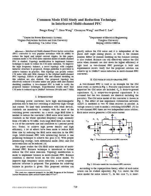
Common Mode EMI Study and Reduction Technique in Interleaved Multi-channel PFCPengju Kong1), 2), Shuo Wang1), Chuanyun Wang1) and Fred C. Lee1)1)Center for Power Electronics Systems, Virginia Polytechnic Institute and State University Blacksburg, VA 24061 USA 2)Department of Electrical EngineeringTsinghua UniversityBeijing 100084 CHINAAbstract— Interleaved Multi-channel Power factor correction (PFC) converter is very popular nowadays with its ability to reduce the input and output current ripples. In this paper, common mode (CM) EMI noise emission model of multi-channel PFC is studied. Topolog y modification to implement balance technique is made to reduce its CM noise emission. To improve the hig h frequency balance, a novel topolog y with coupled-inductor structure is proposed. Desig n g uideline is provided to achieve balance in practice. This topolog y can g reatly reduce CM noise with only little chang es to the orig inal multi-channel PFC topolog y. Effects of phase shift and channel shedding on this solution are also studied. The proposed topolog y has effectively reduced CM noise under any phase shift and channel shedding condition. A two-channel PFC is built to verify the proposed balance technique. Experimental results show that CM noise is reduced up to 20dBuV between 150 kHz and 7 MHz.I.I NTRODUCTIONSwitching power converters have high electromagneticpollution due to their fast switching at relatively high voltageand current. To limit their interference with other devices,standards are mandatory to comply with for most of theswitching power converters. As a result, large EMI filter isneeded to reduce the converter’s EMI noise level below the standards in the whole specified frequency range, normallyfrom 150 kHz to 30 MHz. Such large EMI filter can take upto 1/6 of the converter size and contribute to 1 percent powerloss. Today, to achieve high power density and highefficiency, a lot of efforts have been made to reduce EMIfilter size by reducing the EMI noise emission in the PFC stage. Multi-channel PFC with interleaving feature is one promising technique to achieve this goal [1-4]. With proper interleaving strategy, both differential mode (DM) and CM noise emission can be reduced. [4]This paper studies the CM EMI noise emission of multi-channel PFC. Balance technique is introduced to further reduce the CM noise emission. Topology modification is made to implement balance in multi-channel PFC. Balance condition is derived based on the CM noise model. To improve high frequency noise reduction, a novel coupled-inductor structure is proposed. The guideline for achieving balance in practice is given. This proposed solution canThis work was supported primarily by the ERC Program of the National Science Foundation under Award Number EEC-9731677. greatly reduce the CM noise and it is independent of thephase shift angle among phases, as well as the channelnumber. Effect of channel shedding on this balance solutionis also studied. Balance can still effectively reduce the CMnoise when channels are shut down for higher efficiency at light load. A two-channel PFC prototype is built andexperimental results verify that the proposed solution canachieve up to 20dBuV noise reduction in multi-channel PFCconverters.II.CM NOISE IN MULTI-CHANNEL PFCA two-channel PFC is used as an example for the CM noise study, as shown in Fig. 1. Parasitic capacitances that are important for CM noise are included. C d is drain-to-ground capacitance. C b is output-bus-to-ground capacitance. It is assumed that the two channels are identical including the parasitics. The CM noise model of this converter is shown in Fig. 2. The effect of line impedance stabilization networks (LISN) is modeled as two 50 Ohm resistors in parallel. A voltage source is used to model a switching MOSFET. [5] So in two-channel PFC there are two independent noise sources.Fig. 1. Two-channel interleaved PFC converterdFig. 2. CM noise model for two-channel PFC converter According to the superposition theory, effect of each noise source can be studied separately. Fig. 3(a) shows the CM noise model for noise source V1. In this case V2 is short-circuit. High frequency voltage source V 1 will generate a CM current on the parasitic capacitance C d . This current i CM1 will return through the ground to the LISN and generate a noise voltage on LISN resistors. Effect of V 2 is shown in Fig. 3(b). CM noise current i cm2 is generated by V 2. The sum of two currents is the total CM noise current generated in the two-channel PFC converter.)(21CM CM LISN CM i i R v += (1)v CM1v(a) Effect of V 1 (b) Effect of V 2 Fig. 3. Effect of one noise source on the CM noiseWhen the two channels share the same control signal without any phase shift, they generate the same noise current so that the total current is twice of that in each channel. Interleaving the two channels can cancel some harmonics in the total CM noise current so that CM noise will be reduced. One common practice is to interleave the two channels with 180o phase shift. All the odd order harmonics in i cm1 and i cm2 are out of phase and cancel each other. So that in the total CM noise only the even order harmonics remain. Depending on the switching frequency and EMI specifications, other phase shift angle could be a better choice from the EMI filter size reduction point of view. For example, with 130 kHz switching frequency, also considering 150 kHz startingfrequency of EMI specifications, it is more important to cancel the second harmonic at 260 kHz. In this case 90o phaseshift is preferred. [4]Cancellation of certain harmonics by this means requires accurate control of phase shift angle between channels.General CM noise cancellation concepts, on the other hand,can reduce CM noise in the whole low frequency range up to10 MHz. Several CM noise cancellation techniques havebeen proposed in [5-11]. In this paper, balance technique is applied to reduce the CM noise because of its simple implementation. III. CM NOISE REDUCTION WITH BALANCE TECHNIQUE A. Balance conceptIn Fig. 3(a), V 1 and the inductors, capacitors forms abridge, which allows us to utilize the Wheatstone bridge theory to balance the bridge and minimize the CM noise. This concept is proposed in [5]. A Wheatstone bridge is shown in Figure 4. As long as the impedances on the four bridge legs satisfy the balance condition: 1234Z Z Z Z = (1) the voltage between node M and N will be always zerodisregarding the source V.This Balance concept can be applied to multi-channel PFC converter to reduce its CM noise emission. Balance should be achieved in both Fig. 3(a) and Fig. 3(b) so that effects of V 1 and V 2B. Implementing balance concept in multi-channel PFC converterTopology modification is made to implement balance intwo-channel PFC, as shown in Fig. 5. An inductor is added in the current return path. As a result, the CM noise model is changed as shown in Fig. 6(a). According to the superposition theory, effect of noise source V 1 on CM noise is modeled in Fig. 6(b). L L D 1D 2D 3D 4V ACC d C dC b L bFig. 5. Two-channel PFC with balance technique V 1V 2C b C d C dL LL bV 1C bC d C dL LL b(a) CM noise model (b) Effect of V 1Fig. 6. CM noise model of two-channel PFC with balance techniqueIn Fig. 6(b), L b and L are in parallel. So do C b and C d . To minimize the effect of V 1 on CM noise, balance condition should be achieved: Cb Cd Cd L Lb LZ Z Z Z ////=(3) Eq. 3 is also the balance condition for noise source V 2, since the model for the effect of V 2 is the same in topology asthat of V 1. As a result, achieving balance in two-channel PFC can reduce the CM noise in both channels, disregarding the phase shift angle between the two sources.In frequency range below 2 MHz, the impedances of inductors are determined by the inductance and the impedances of parasitic capacitances are determined by the capacitance values. Balance can be achieved by designing L b value based on L and parasitic capacitance values. C. Coupled-inductor structure to achieve balance at high frequencyAlthough balance can be achieved by controlling L b at low frequency, it is not possible to control the parasitics for high frequency balance. Fig. 7 shows the equivalent model of boost inductor including its equivalent parallel capacitance (EPC) and equivalent parallel resistance (EPR). Beyond 2 MHz, EPC and EPR become dominant in impedance for boost inductors. Balance condition is no longer achieved. Although it is possible to achieve balance by compensating EPC and EPR with extra capacitors and resistors, the resulted large EPC will increase the high frequency DM noise. [12]LEPCEPRFig. 7. Model of an inductor considering high frequency parasticsIn single channel PFC, the added inductor is coupled with the boost inductor to solve the high frequency balance issue [5]. The coupling coefficient should be high to achieve better performance at high frequency. However, in multi-channel PFC converter where more than one boost inductors need to be coupled with the added inductor L b , it becomes complicated. A novel coupled-inductor structure is proposed in multi-channel PFC converters to achieve high frequencybalance. One winding is added in the boost inductor in eachchannel. And these windings are inserted in series in the current return path, as shown in Fig. 8(a). Fig. 8(b) shows its CM noise model. Fig. 9(a) shows the effect of V 1. To studyits balance condition, an equivalent decoupled model is usedfor this model, as shown in Fig. 9(b).V(a) Proposed multi-channel PFC topology with balance technique andcoupled-inductor structure(b) CM noise modelFig. 8 Proposed multi-channel PFC topology with balance technique andcoupled-inductor structured(a) CM noise model with only the effect of V 1(b) Equivalent decoupled model Fig. 9 CM noise model for one noise source and its equivalent decoupled model The ratio of Z a and Z b can be derived by matching the impedances of Fig. 9(a) and Fig. 9(b). Assume that couplingcoefficients between L and L a are unity, and the turns for windings L and L b are N1 and N2, the voltages and the currents across the windings have the relation as shown inEq. 4.⎪⎪⎪⎭⎪⎪⎪⎬⎫==+−==2111112121i i V V V N N V V N N V V n n m n n m m(4)The ratio of Z a and Z b can be derived from Eq. 4.121//21+==N N i V i V Z Z n m b a (5)Substitute (5) into (3), the balance condition for noise source V 1 is,d b C C N N =21 (6) According to Eq. 4 and 6, with high coupling coefficient between L and L b , the balance condition is determined only by the turns ratio, effects of EPC and EPR are eliminated. The same procedure can be done to derive the balance condition for V 2. Since the inductor L and parasitic capacitance C d in all channels are the same, Eq. 6 is also the balance condition for noise source V 2. It is for both noise source and independent on the relation of V 1 and V 2. As long as this balance condition is achieved, CM noise in the two-channel PFC can be minimized.D. Achieving balance in N-channel PFCThe balance technique can be extended to multi-channel PFC with any channel number. Assume the channel number is N, there will be N noise sources in the model. Again superposition theory is used to analyze the effect of any one of the noise source. The CM noise model with one noise source is shown in Fig. 10(a). Following the same procedure, an equivalent decoupled model is introduced and shown in Fig. 10(b). Balance condition for this N-channel PFC model is1−+=N C C Z Z db bNaN(7).dd(b) CM noise model for N-channel PFCd(b) Equivalent decoupled modelFig. 10 CM noise model for N-channel PFC and its equivalent decoupledmodelThe ratio of Z aN and Z bN can be derived following the sameprocedure.⎪⎪⎪⎪⎭⎪⎪⎪⎪⎪⎬⎫==−=−==∑−=21112121...2121i i V V N N V V N N V V N N V V n x x n m (8)121//21−+==N N N i V i V Z Z m bNaN (9)The balance condition for N-channel PFC is derived by substitute (9) into (7). And it becomes the same as Eq. 6. The same conclusion can be derived for any other noise source. This balance condition can reduce the total CM noise of N-channel PFC converter and independent of the channel number.E. Implementing balance in practiceIn practice, Balance condition can be achieved in the multi-channel PFC converter by adjusting either turns ratio or parasitic capacitances according to Eq. 6. One method is to determine N2 according to the parasitic capacitances C b and C d . In PFC converters, C b is usually more than 10 times of C d . According to Eq. 6, N 2 is very small compared to N1. So in the implementation, a winding of 2 to 4 turns is needed to add on each boost inductor. Another method is to predetermine a proper turns ratio, and adjust C b or C d to achieve balance.According to the analysis in [5], high turns ratio is preferred to achieve better balance. To achieve high turns ratio, N2 should be minimized to be 1 turn. In this case, to achieve balance, extra capacitor is added between output bus and ground to increase C b .Another benefit of high turns ratio is that it avoids possible increase of the channel current ripple. In this coupled-inductor structure, the boost inductors in all channels are indirectly coupled. This coupling among channels will affect the channel current ripples of the converter. Such coupling effect is discussed and widely used in voltage regulation module (VRM) applications. [13] In the VRM application, take two-channel interleaved buck converter for example, the two inductors are reverse coupled, as shown in Fig. 11. The channel current ripple is reduced. However, in the proposed PFC application, the coupling polarity is the opposite and the channel current ripple will be increased. The strongercoupling between two channels, the larger channel current ripple does the converter have, which is not desirable. To estimate the coupling effect, coupling coefficient between two channels in boost PFC converter can be derived by calculating the equivalent self-inductance L e in each channel and mutual inductance M e between the two channels, as given in Eq. 10 and 11. Assuming the coupling coefficient between L and L b is unity, the equivalent coupling coefficient between two channels can be calculated in Eq. 12.b e L M L L 22++= (10)b e L M M 22+= (11) 22222+++==n n n L M k e e e (12) where M is the mutual inductance between L and L b , n is the turns ratio of L and L b , n=N1/N2. It can be seen from Eq. 12 that lower turns ratio results in higher equivalent coupling coefficient between channels, so that channel current ripple will be larger. High turns ratio is preferred from this perspective to maintain relatively lowchannel ripple. Fig. 12 shows the simulation results of thecurrent ripple comparison with different turns ratios. When turns ratio is 30, the channel current ripple is close to the non-couple inductors case. When the turns ratio is 10, channelFig. 11 Coupled inductors in multi-channel Buck converterFig. 12 Channel current ripple with different turns ratio nIn practice, with imperfect coupling, balance condition is not only determined by the turns ratio but also the coupling coefficient, in which case parasitic capacitance can be fine-tuned to achieve balance. Coupling coefficient between L andL b should be higher than 0.7 for achieving balance up to 10 MHz.F. Channel shedding and its effect on balanceOne benefit of multi-channel PFC compared to single channel one is the possibility to shut down channels at different load condition for the purpose of improving light load efficiency. The proposed balance implementation can still reduce CM noise with any number of channel shedding. Take a three-channel PFC with one channel shut down for example. The MOSFET and diode remain off in the shut-down channel. They can be replaced by their junction capacitance, as shown in Fig. 13(a). The CM noise model is shown in Fig. 13(b). It is no longer a Wheatstone bridge sothat the equivalent decoupled model is not applicable foranalysis. The CM noise can be analyzed from the CM current cancellation point of view. Assume the coupling coefficient between L and L bis unity, the voltages on them can becalculated in Eq. 13. 21332211N NV V V V V V m m m −=== (13) These voltages are fast switching voltages and introduce CM noise current through parasitic capacitances C d and C b :⎪⎪⎪⎪⎭⎪⎪⎪⎪⎬⎫===++=dt dV C i dt dV C i dtdV C i dtV V V d C i m dd m dd m dd bb 332211321)( (14). The total CM current is the sum of these currents, as shownin Eq. 14.dtV V V d C dt V V V d C i i i i i i m m m d b d d d b CM )()(321321321++⋅+++⋅=+++==∑ (15)Substituting Eq. 13 into Eq. 15, condition for CM noisecurrent cancellation can be derived, which is exactly the same as Eq. 6. In conclusion, channel shedding does not change the ability of the balance approach in reducing CM noise. The same conclusion can be made in N-channel PFC converter with any number of shut-down channels.Vbdddiodem3d3(b) CM noise modelFig. 13 3-channel PFC with one channel shut down and its CM modelIII . E XPERIMENTAL RESULTA 1.2kW two-channel boost PFC converter is built to validate the proposed method. The input voltage is 110 Vac and the output is 400 Vdc. The switching frequency is 130 kHz in each channel. Boost inductance L in each channel is 330uH, implemented using toriodal core with 62 turns. Parasitic capacitances of the converter are measured. C d is 5.8pF and C b is 194pF. CM noises are measured and compared.First, the original CM noise of two-channel 180o -phase-shift PFC converter is measured and shown in Fig. 14. The first order and third order harmonics, which is 130 kHz and 390 kHz respectively, are cancelled and significantly lower than the even order harmonics. Then balance is achieved by adding a 10uH inductor, as shown in Fig. 5, to verify the balance effect at low frequency and the high frequency issue. In Fig. 14, the measurement result shows that CM noise below 2 MHz is greatly reduced but high frequency noise remains and even increased around 4 MHz.Then coupled-inductor structure is implemented to improve the high frequency noise reduction. A winding of 2 turns (N2 = 2) are added on each toriadal core to implement L b so that balance condition is satisfied. The measured CM noise is shown in Fig. 15. It is reduced as much as 20dBuV from 150 kHz up to 7 MHz. However, noise beyond 7 MHz is even worse than the original noise.Another implementation of L b is to use 1 turn (N2 = 1) to get higher turns ratio and 176pF is added between the output bus of PFC and ground to achieve balance. Figure 16 shows the measured CM noise with different N2 (turns ratio). It can be seen that when N2 is 1, which means higher turns ratio, high frequency CM noise is lower.In both cases, the parasitic capacitance ratio is not accurately equal to the turns ratio due to imperfect coupling coefficient. Fine-tune is done on C b value to achieve best noise reduction.Figure 17 shows the CM noise with balance technique when the two channels have different phase shift angle. It is shown that phase shift does not affect the balance result. Fig. 18 shows the effect of channel shedding. When one channel is shut down, low frequency CM noise remains at the same level and the high frequency noise is even lower.Frequency (Hz)C M n o s i e (d B u V )Fig. 14 Effect of balance on CM noise, without coupled-inductors101010Frequency (Hz)C M n o i s e (d B u V )Fig. 15 Effect of balance on CM noise, with coupled-inductors101010Frequency (Hz)C M n o i s e (d B u V )Fig. 16 Effect of N2 (turns ratio) on CM noise1010Frequency (Hz)C M n o i s e (d B u V )Fig. 17. Effect of phase shift on balance1010Frequency (Hz)C M n o i s e (d B u V )Fig. 18. CM noise when one phase is shut downIV . C ONCLUSIONIn this paper, balance technique is introduced to reduce the CM noise in multi-channel PFC converter. The CM noise emission model of multi-channel PFC converter is derived. Balance technique is implemented in the converter and the balance condition is derived. To improve the high frequency CM noise, coupled-inductor structure is proposed to eliminate the effect of parasitics. This solution can greatly reduce CM noise and is independent of phase shift and channel number. This solution also works well when some of the channels are shut down for higher efficiency at light load. Experiments have been done to verify the proposed method. CM noise in multi-channel PFC with balance technique can be greatly reduced up to 20 MHz from 150 kHz to 7 MHz.R EFERENCES[1] M. O’Loughlin, “350-W, two-phase interleaved PFC pre-regulator designreview”, SLUA369A-August 2006[2] B.A. Miwa, D.M. Otten, M.E. Schlecht, “High efficiency power factorcorrection using interleaving techniques”, APEC 1992. pp. 557 - 568[3] R.L. Barnett, B.O. Blair, G.H. Fasullo, D. Marabell, A. Marsh,“Interleaved converter power factor correction method and apparatus,” United States Patent #6,690,589 B2, Feb. 10, 2004[4] C. Wang, M. Xu, F.C. Lee, and B. Lu, “EMI study for the interleavedmulti-channel PFC”, PESC 2007, pp. 1336 - 1342[5] S. Wang, P. Kong and F.C. Lee, “Common mode noise reduction forboost converters using general balance technique”, IEEE transactions on power electronics, Vol. 22, No.4, pp. 1410 – 1416, July 2007[6] X. Wu, N.K. Poon, C.M. Lee, M.H. Poon and Z. Qian, “A study ofcommon mode noise in switching power supply from a current balancing viewpoint,” proc. of IEEE International Conference on Power Electronics and Drive Systems, July 1999, Vol. 2, pp. 621 – 625. [7] D. Cochrane, D. Chen, and D. Boroyevich, “Passive cancellation ofcommon-mode noise in power electronic circuits,” IEEE Transaction on Power Electronics, Vol. 18, Issue 3, pp. 756 – 763, May 2003.[8] M. Crosato and I. Hofsajer, “Minimising conducted common mode EMIby charge balancing in a nonisolated DC-DC converter,” proc. of IEEE Power Electronics Specialist Conference, 2004, Vol. 4, pp. 3146 – 3151. [9] M. Shoyama, L. Ge and T. Ninomiya, “Balanced switching converter toreduce common mode conducted noise,” IEEE Transactions on Industrial Electronics, Vol. 50, No. 6, pp. 1095-1099, Dec. 2003.[10] M. Borage, S. Tiwari, and S. Kotaiah, “Common-mode noise sourceand its passive cancellation in full-bridge resonant converter,” proc. of IEEE 8th International Conference on Electromagnetic Interference and Compatibility, INCEMIC 2003, Dec. 2003, pp. 9 - 14. [11] S. Lin, M. Zhou, W. Chen and J. Ying, “Novel methods to reducecommon-mode noise based on noise balance,” proc. of IEEE Power Electronics Specialist Conference, 2006, pp. 2728 – 2733.[12] S. Wang, F.C. Lee, W.G. Odendaal, “Improving the performance ofboost PFC EMI filters”, APEC 2003, Vol. 1, pp. 368-374[13] P. Wong, P. Xu, P. Yang, F.C. Lee, Performance improvements ofinterleaving VRMs with coupling inductors, IEEE transactions on power electronics, Vol. 16, Issue.4, pp. 499 – 507, July 2001。

1. Automation in this true sense is brought to full fruition only through a thorough exploitation of its three major elements, communication, computation, and control----the three “Cs”.自动化按其确切的意义,只有全面运用通信、计算和控制三个主要组成部分(“三C" )才能完全实现。
2. In the case of the blast-furnace, the computer would need to be supplied with information about the raw material which goes into the furnace, the temperatures at which the furnace works, and the best way of dealing with the various ingredients.就高炉来说,需要给计算机提供装人高炉的原料的信息、高炉工作温度的信息和处理各种各样配料的最好方法等方面的资料。
3. The operation of this part of the steel plant is a complex and highly skilled operation, requiringa great deal of knowledge, a great deal of integrated information and rapid decision-making, to make sure the furnace operates efficiently in relation to the next stage in the process.钢厂的高炉操作是一项复杂而要求技术熟练的作业,需要大量的知识和大量的综合信息,并迅速地做出判定选择,以便确保高炉工艺流程中的下一阶段的有效工作。

Semiconductor Manufacturing Technology半导体制造技术Instructor’s ManualMichael QuirkJulian SerdaCopyright Prentice HallTable of Contents目录OverviewI. Chapter1. Semiconductor industry overview2. Semiconductor materials3. Device technologies—IC families4. Silicon and wafer preparation5. Chemicals in the industry6. Contamination control7. Process metrology8. Process gas controls9. IC fabrication overview10. Oxidation11. Deposition12. Metallization13. Photoresist14. Exposure15. Develop16. Etch17. Ion implant18. Polish19. Test20. Assembly and packagingII. Answers to End-of-Chapter Review QuestionsIII. Test Bank (supplied on diskette)IV. Chapter illustrations, tables, bulleted lists and major topics (supplied on CD-ROM)Notes to Instructors:1)The chapter overview provides a concise summary of the main topics in each chapter.2)The correct answer for each test bank question is highlighted in bold. Test bankquestions are based on the end-of-chapter questions. If a student studies the end-of-chapter questions (which are linked to the italicized words in each chapter), then they will be successful on the test bank questions.2Chapter 1Introduction to the Semiconductor Industry Die:管芯 defective:有缺陷的Development of an Industry•The roots of the electronic industry are based on the vacuum tube and early use of silicon for signal transmission prior to World War II. The first electronic computer, the ENIAC, wasdeveloped at the University of Pennsylvania during World War II.•William Shockley, John Bardeen and Walter Brattain invented the solid-state transistor at Bell Telephone Laboratories on December 16, 1947. The semiconductor industry grew rapidly in the 1950s to commercialize the new transistor technology, with many early pioneers working inSilicon Valley in Northern California.Circuit Integration•The first integrated circuit, or IC, was independently co-invented by Jack Kilby at Texas Instruments and Robert Noyce at Fairchild Semiconductor in 1959. An IC integrates multiple electronic components on one substrate of silicon.•Circuit integration eras are: small scale integration (SSI) with 2 - 50 components, medium scale integration (MSI) with 50 – 5k components, large scale integration (LSI) with 5k to 100kcomponents, very large scale integration (VLSI) with 100k to 1M components, and ultra large scale integration (ULSI) with > 1M components.1IC Fabrication•Chips (or die) are fabricated on a thin slice of silicon, known as a wafer (or substrate). Wafers are fabricated in a facility known as a wafer fab, or simply fab.•The five stages of IC fabrication are:Wafer preparation: silicon is purified and prepared into wafers.Wafer fabrication: microchips are fabricated in a wafer fab by either a merchant chip supplier, captive chip producer, fabless company or foundry.Wafer test: Each individual die is probed and electrically tested to sort for good or bad chips.Assembly and packaging: Each individual die is assembled into its electronic package.Final test: Each packaged IC undergoes final electrical test.•Key semiconductor trends are:Increase in chip performance through reduced critical dimensions (CD), more components per chip (Moore’s law, which predicts the doubling of components every 18-24 months) andreduced power consumption.Increase in chip reliability during usage.Reduction in chip price, with an estimated price reduction of 100 million times for the 50 years prior to 1996.The Electronic Era•The 1950s saw the development of many different types of transistor technology, and lead to the development of the silicon age.•The 1960s were an era of process development to begin the integration of ICs, with many new chip-manufacturing companies.•The 1970s were the era of medium-scale integration and saw increased competition in the industry, the development of the microprocessor and the development of equipment technology. •The 1980s introduced automation into the wafer fab and improvements in manufacturing efficiency and product quality.•The 1990s were the ULSI integration era with the volume production of a wide range of ICs with sub-micron geometries.Career paths•There are a wide range of career paths in semiconductor manufacturing, including technician, engineer and management.2Chapter 2 Characteristics of Semiconductor MaterialsAtomic Structure•The atomic model has three types of particles: neutral neutrons(不带电的中子), positively charged protons(带正电的质子)in the nucleus and negatively charged electrons(带负电的核外电子) that orbit the nucleus. Outermost electrons are in the valence shell, and influence the chemical and physical properties of the atom. Ions form when an atom gains or loses one or more electrons.The Periodic Table•The periodic table lists all known elements. The group number of the periodic table represents the number of valence shell electrons of the element. We are primarily concerned with group numbers IA through VIIIA.•Ionic bonds are formed when valence shell electrons are transferred from the atoms of one element to another. Unstable atoms (e.g., group VIIIA atoms because they lack one electron) easily form ionic bonds.•Covalent bonds have atoms of different elements that share valence shell electrons.3Classifying Materials•There are three difference classes of materials:ConductorsInsulatorsSemiconductors•Conductor materials have low resistance to current flow, such as copper. Insulators have high resistance to current flow. Capacitance is the storage of electrical charge on two conductive plates separated by a dielectric material. The quality of the insulation material between the plates is the dielectric constant. Semiconductor materials can function as either a conductor or insulator.Silicon•Silicon is an elemental semiconductor material because of four valence shell electrons. It occurs in nature as silica and is refined and purified to make wafers.•Pure silicon is intrinsic silicon. The silicon atoms bond together in covalent bonds, which defines many of silicon’s properties. Silicon atoms bond together in set, repeatable patterns, referred to asa crystal.•Germanium was the first semiconductor material used to make chips, but it was soon replaced by silicon. The reasons for this change are:Abundance of siliconHigher melting temperature for wider processing rangeWide temperature range during semiconductor usageNatural growth of silicon dioxide•Silicon dioxide (SiO2) is a high quality, stable electrical insulator material that also serves as a good chemical barrier to protect silicon from external contaminants. The ability to grow stable, thin SiO2 is fundamental to the fabrication of Metal-Oxide-Semiconductor (MOS) devices. •Doping increases silicon conductivity by adding small amounts of other elements. Common dopant elements are from trivalent, p-type Group IIIA (boron) and pentavalent, n-type Group VA (phosphorus, arsenic and antimony).•It is the junction between the n-type and p-type doped regions (referred to as a pn junction) that permit silicon to function as a semiconductor.4Alternative Semiconductor Materials•The alternative semiconductor materials are primarily the compound semiconductors. They are formed from Group IIIA and Group VA (referred to as III-V compounds). An example is gallium arsenide (GaAs).•Some alternative semiconductors come from Group IIA and VIA, referred to as II-VI compounds. •GaAs is the most common III-V compound semiconductor material. GaAs ICs have greater electron mobility, and therefore are faster than ICs made with silicon. GaAs ICs also have higher radiation hardness than silicon, which is better for space and military applications. The primary disadvantage of GaAs is the lack of a natural oxide.5Chapter 3Device TechnologiesCircuit Types•There are two basic types of circuits: analog and digital. Analog circuits have electrical data that varies continuously over a range of voltage, current and power values. Digital circuits have operating signals that vary about two distinct voltage levels – a high and a low.Passive Component Structures•Passive components such as resistors and capacitors conduct electrical current regardless of how the component is connected. IC resistors are a passive component. They can have unwanted resistance known as parasitic resistance. IC capacitor structures can also have unintentional capacitanceActive Component Structures•Active components, such as diodes and transistors can be used to control the direction of current flow. PN junction diodes are formed when there is a region of n-type semiconductor adjacent to a region of p-type semiconductor. A difference in charge at the pn junction creates a depletion region that results in a barrier voltage that must be overcome before a diode can be operated. A bias voltage can be configured to have a reverse bias, with little or no conduction through the diode, or with a forward bias, which permits current flow.•The bipolar junction transistor (BJT) has three electrodes and two pn junctions. A BJT is configured as an npn or pnp transistor and biased for conduction mode. It is a current-amplifying device.6• A schottky diode is formed when metal is brought in contact with a lightly doped n-type semiconductor material. This diode is used in faster and more power efficient BJT circuits.•The field-effect transistor (FET), a voltage-amplifying device, is more compact and power efficient than BJT devices. A thin gate oxide located between the other two electrodes of the transistor insulates the gate on the MOSFET. There are two categories of MOSFETs, nMOS (n-channel) and pMOS (p-channel), each which is defined by its majority current carriers. There is a biasing scheme for operating each type of MOSFET in conduction mode.•For many years, nMOS transistors have been the choice of most IC manufacturers. CMOS, with both nMOS and pMOS transistors in the same IC, has been the most popular device technology since the early 1980s.•BiCMOS technology makes use of the best features of both CMOS and bipolar technology in the same IC device.•Another way to categorize FETs is in terms of enhancement mode and depletion mode. The major different is in the way the channels are doped: enhancement-mode channels are doped opposite in polarity to the source and drain regions, whereas depletion mode channels are doped the same as their respective source and drain regions.Latchup in CMOS Devices•Parasitic transistors can create a latchup condition(???????) in CMOS ICs that causes transistors to unintentionally(无心的) turn on. To control latchup, an epitaxial layer is grown on the wafer surface and an isolation barrier(隔离阻障)is placed between the transistors. An isolation layer can also be buried deep below the transistors.Integrated Circuit Productsz There are a wide range of semiconductor ICs found in electrical and electronic products. This includes the linear IC family, which operates primarily with anal3og circuit applications, and the digital IC family, which includes devices that operate with binary bits of data signals.7Chapter 4Silicon and Wafer Preparation8z Semiconductor-Grade Silicon•The highly refined silicon used for wafer fabrication is termed semiconductor-grade silicon (SGS), and sometimes referred to as electronic-grade silicon. The ultra-high purity of semiconductor-grade silicon is obtained from a multi-step process referred to as the Siemens process.Crystal Structure• A crystal is a solid material with an ordered, 3-dimensional pattern over a long range. This is different from an amorphous material that lacks a repetitive structure.•The unit cell is the most fundamental entity for the long-range order found in crystals. The silicon unit cell is a face-centered cubic diamond structure. Unit cells can be organized in a non-regular arrangement, known as a polycrystal. A monocrystal are neatly arranged unit cells.Crystal Orientation•The orientation of unit cells in a crystal is described by a set of numbers known as Miller indices.The most common crystal planes on a wafer are (100), (110), and (111). Wafers with a (100) crystal plane orientation are most common for MOS devices, whereas (111) is most common for bipolar devices.Monocrystal Silicon Growth•Silicon monocrystal ingots are grown with the Czochralski (CZ) method to achieve the correct crystal orientation and doping. A CZ crystal puller is used to grow the silicon ingots. Chunks of silicon are heated in a crucible in the furnace of the puller, while a perfect silicon crystal seed is used to start the new crystal structure.• A pull process serves to precisely replicate the seed structure. The main parameters during the ingot growth are pull rate and crystal rotation. More homogeneous crystals are achieved with a magnetic field around the silicon melt, known as magnetic CZ.•Dopant material is added to the melt to dope the silicon ingot to the desired electrical resistivity.Impurities are controlled during ingot growth. A float-zone crystal growth method is used toachieve high-purity silicon with lower oxygen content.•Large-diameter ingots are grown today, with a transition underway to produce 300-mm ingot diameters. There are cost benefits for larger diameter wafers, including more die produced on a single wafer.Crystal Defects in Silicon•Crystal defects are interruptions in the repetitive nature of the unit cell. Defect density is the number of defects per square centimeter of wafer surface.•Three general types of crystal defects are: 1) point defects, 2) dislocations, and 3) gross defects.Point defects are vacancies (or voids), interstitial (an atom located in a void) and Frenkel defects, where an atom leaves its lattice site and positions itself in a void. A form of dislocation is astacking fault, which is due to layer stacking errors. Oxygen-induced stacking faults are induced following thermal oxidation. Gross defects are related to the crystal structure (often occurring during crystal growth).Wafer Preparation•The cylindrical, single-crystal ingot undergoes a series of process steps to create wafers, including machining operations, chemical operations, surface polishing and quality checks.•The first wafer preparation steps are the shaping operations: end removal, diameter grinding, and wafer flat or notch. Once these are complete, the ingot undergoes wafer slicing, followed by wafer lapping to remove mechanical damage and an edge contour. Wafer etching is done to chemically remove damage and contamination, followed by polishing. The final steps are cleaning, wafer evaluation and packaging.Quality Measures•Wafer suppliers must produce wafers to stringent quality requirements, including: Physical dimensions: actual dimensions of the wafer (e.g., thickness, etc.).Flatness: linear thickness variation across the wafer.Microroughness: peaks and valleys found on the wafer surface.Oxygen content: excessive oxygen can affect mechanical and electrical properties.Crystal defects: must be minimized for optimum wafer quality.Particles: controlled to minimize yield loss during wafer fabrication.Bulk resistivity(电阻系数): uniform resistivity from doping during crystal growth is critical. Epitaxial Layer•An epitaxial layer (or epi layer) is grown on the wafer surface to achieve the same single crystal structure of the wafer with control over doping type of the epi layer. Epitaxy minimizes latch-up problems as device geometries continue to shrink.Chapter 5Chemicals in Semiconductor FabricationEquipment Service Chase Production BayChemical Supply Room Chemical Distribution Center Holding tank Chemical drumsProcess equipmentControl unit Pump Filter Raised and perforated floorElectronic control cablesSupply air ductDual-wall piping for leak confinement PumpFilterChemical control and leak detection Valve boxes for leak containment Exhaust air ductStates of Matter• Matter in the universe exists in 3 basic states (宇宙万物存在着三种基本形态): solid, liquid andgas. A fourth state is plasma.Properties of Materials• Material properties are the physical and chemical characteristics that describe its unique identity.• Different properties for chemicals in semiconductor manufacturing are: temperature, pressure andvacuum, condensation, vapor pressure, sublimation and deposition, density, surface tension, thermal expansion and stress.Temperature is a measure of how hot or cold a substance is relative to another substance. Pressure is the force exerted per unit area. Vacuum is the removal of gas molecules.Condensation is the process of changing a gas into a liquid. Vaporization is changing a liquidinto a gas.Vapor pressure is the pressure exerted by a vapor in a closed container at equilibrium.Sublimation is the process of changing a solid directly into a gas. Deposition is changing a gas into a solid.Density is the mass of a substance divided by its volume.Surface tension of a liquid is the energy required to increase the surface area of contact.Thermal expansion is the increase in an object’s dimension due to heating.Stress occurs when an object is exposed to a force.Process Chemicals•Semiconductor manufacturing requires extensive chemicals.• A chemical solution is a chemical mixture. The solvent is the component of the solution present in larger amount. The dissolved substances are the solutes.•Acids are solutions that contain hydrogen and dissociate in water to yield hydronium ions. A base is a substance that contains the OH chemical group and dissociates in water to yield the hydroxide ion, OH-.•The pH scale is used to assess the strength of a solution as an acid or base. The pH scale varies from 0 to 14, with 7 being the neutral point. Acids have pH below 7 and bases have pH values above 7.• A solvent is a substance capable of dissolving another substance to form a solution.• A bulk chemical distribution (BCD) system is often used to deliver liquid chemicals to the process tools. Some chemicals are not suitable for BCD and instead use point-of-use (POU) delivery, which means they are stored and used at the process station.•Gases are generally categorized as bulk gases or specialty gases. Bulk gases are the relatively simple gases to manufacture and are traditionally oxygen, nitrogen, hydrogen, helium and argon.The specialty gases, or process gases, are other important gases used in a wafer fab, and usually supplied in low volume.•Specialty gases are usually transported to the fab in metal cylinders.•The local gas distribution system requires a gas purge to flush out undesirable residual gas. Gas delivery systems have special piping and connections systems. A gas stick controls the incoming gas at the process tool.•Specialty gases may be classified as hydrides, fluorinated compounds or acid gases.Chapter 6Contamination Control in Wafer FabsIntroduction•Modern semiconductor manufacturing is performed in a cleanroom, isolated from the outside environment and contaminants.Types of contamination•Cleanroom contamination has five categories: particles, metallic impurities, organic contamination, native oxides and electrostatic discharge. Killer defects are those causes of failure where the chip fails during electrical test.Particles: objects that adhere to a wafer surface and cause yield loss. A particle is a killer defect if it is greater than one-half the minimum device feature size.Metallic impurities: the alkali metals found in common chemicals. Metallic ions are highly mobile and referred to as mobile ionic contaminants (MICs).Organic contamination: contains carbon, such as lubricants and bacteria.Native oxides: thin layer of oxide growth on the wafer surface due to exposure to air.Electrostatic discharge (ESD): uncontrolled transfer of static charge that can damage the microchip.Sources and Control of Contamination•The sources of contamination in a wafer fab are: air, humans, facility, water, process chemicals, process gases and production equipment.Air: class number designates the air quality inside a cleanroom by defining the particle size and density.Humans: a human is a particle generator. Humans wear a cleanroom garment and follow cleanroom protocol to minimize contamination.Facility: the layout is generally done as a ballroom (open space) or bay and chase design.Laminar airflow with air filtering is used to minimize particles. Electrostatic discharge iscontrolled by static-dissipative materials, grounding and air ionization.Ultrapure deiniozed (DI) water: Unacceptable contaminants are removed from DI water through filtration to maintain a resistivity of 18 megohm-cm. The zeta potential represents a charge on fine particles in water, which are trapped by a special filter. UV lamps are used for bacterial sterilization.Process chemicals: filtered to be free of contamination, either by particle filtration, microfiltration (membrane filter), ultrafiltration and reverse osmosis (or hyperfiltration).Process gases: filtered to achieve ultraclean gas.Production equipment: a significant source of particles in a fab.Workstation design: a common layout is bulkhead equipment, where the major equipment is located behind the production bay in the service chase. Wafer handling is done with robotic wafer handlers. A minienvironment is a localized environment where wafers are transferred on a pod and isolated from contamination.Wafer Wet Cleaning•The predominant wafer surface cleaning process is with wet chemistry. The industry standard wet-clean process is the RCA clean, consisting of standard clean 1 (SC-1) and standard clean 2 (SC-2).•SC-1 is a mixture of ammonium hydroxide, hydrogen peroxide and DI water and capable of removing particles and organic materials. For particles, removal is primarily through oxidation of the particle or electric repulsion.•SC-2 is a mixture of hydrochloric acid, hydrogen peroxide and DI water and used to remove metals from the wafer surface.•RCA clean has been modified with diluted cleaning chemistries. The piranha cleaning mixture combines sulfuric acid and hydrogen peroxide to remove organic and metallic impurities. Many cleaning steps include an HF last step to remove native oxide.•Megasonics(兆声清洗) is widely used for wet cleaning. It has ultrasonic energy with frequencies near 1 MHz. Spray cleaning will spray wet-cleaning chemicals onto the wafer. Scrubbing is an effective method for removing particles from the wafer surface.•Wafer rinse is done with overflow rinse, dump rinse and spray rinse. Wafer drying is done with spin dryer or IPA(异丙醇) vapor dry (isopropyl alcohol).•Some alternatives to RCA clean are dry cleaning, such as with plasma-based cleaning, ozone and cryogenic aerosol cleaning.Chapter 7Metrology and Defect InspectionIC Metrology•In a wafer fab, metrology refers to the techniques and procedures for determining physical and electrical properties of the wafer.•In-process data has traditionally been collected on monitor wafers. Measurement equipment is either stand-alone or integrated.•Yield is the percent of good parts produced out of the total group of parts started. It is an indicator of the health of the fabrication process.Quality Measures•Semiconductor quality measures define the requirements for specific aspects of wafer fabrication to ensure acceptable device performance.•Film thickness is generally divided into the measurement of opaque film or transparent film. Sheet resistance measured with a four-point probe is a common method of measuring opaque films (e.g., metal film). A contour map shows sheet resistance deviations across the wafer surface.•Ellipsometry is a nondestructive, noncontact measurement technique for transparent films. It works based on linearly polarized light that reflects off the sample and is elliptically polarized.•Reflectometry is used to measure a film thickness based on how light reflects off the top and bottom surface of the film layer. X-ray and photoacoustic technology are also used to measure film thickness.•Film stress is measured by analyzing changes in the radius of curvature of the wafer. Variations in the refractive index are used to highlight contamination in the film.•Dopant concentration is traditionally measured with a four-point probe. The latest technology is the thermal-wave system, which measures the lattice damage in the implanted wafer after ion implantation. Another method for measuring dopant concentration is spreading resistance probe. •Brightfield detection is the traditional light source for microscope equipment. An optical microscope uses light reflection to detect surface defects. Darkfield detection examines light scattered off defects on the wafer surface. Light scattering uses darkfield detection to detectsurface particles by illuminating the surface with laser light and then using optical imaging.•Critical dimensions (CDs) are measured to achieve precise control over feature size dimensions.The scanning electron microscope is often used to measure CDs.•Conformal step coverage is measured with a surface profiler that has a stylus tip.•Overlay registration measures the ability to accurately print photoresist patterns over a previously etched pattern.•Capacitance-voltage (C-V) test is used to verify acceptable charge conditions and cleanliness at the gate structure in a MOS device.Analytical Equipment•The secondary-ion mass spectrometry (SIMS) is a method of eroding a wafer surface with accelerated ions in a magnetic field to analyze the surface material composition.•The atomic force microscope (AFM) is a surface profiler that scans a small, counterbalanced tip probe over the wafer to create a 3-D surface map.•Auger electron spectroscopy (AES) measures composition on the wafer surface by measuring the energy of the auger electrons. It identifies elements to a depth of about 2 nm. Another instrument used to identify surface chemical species is X-ray photoelectron spectroscopy (XPS).•Transmission electron microscopy (TEM) uses a beam of electrons that is transmitted through a thin slice of the wafer. It is capable of quantifying very small features on a wafer, such as silicon crystal point defects.•Energy-dispersive spectrometer (EDX) is a widely used X-ray detection method for identifying elements. It is often used in conjunction with the SEM.• A focused ion beam (FIB) system is a destructive technique that focuses a beam of ions on the wafer to carve a thin cross section from any wafer area. This permits analysis of the wafermaterial.Chapter 8Gas Control in Process ChambersEtch process chambers••The process chamber is a controlled vacuum environment where intended chemical reactions take place under controlled conditions. Process chambers are often configured as a cluster tool. Vacuum•Vacuum ranges are low (rough) vacuum, medium vacuum, high vacuum and ultrahigh vacuum (UHV). When pressure is lowered in a vacuum, the mean free path(平均自由行程) increases, which is important for how gases flow through the system and for creating a plasma.Vacuum Pumps•Roughing pumps are used to achieve a low to medium vacuum and to exhaust a high vacuum pump. High vacuum pumps achieve a high to ultrahigh vacuum.•Roughing pumps are dry mechanical pumps or a blower pump (also referred to as a booster). Two common high vacuum pumps are a turbomolecular (turbo) pump and cryopump. The turbo pump is a reliable, clean pump that works on the principle of mechanical compression. The cryopump isa capture pump that removes gases from the process chamber by freezing them.。
电力电子技术Power Electronics 第55卷第2期2021年2月Vol.55, No.2February 2021简化矢量的多电平逆变器共模电压抑制方法刘战,卢凯尔,李飞,夏正龙(江苏师范大学,电气工程及自动化学院,江苏徐州221116)摘要:在高压变频传动领域,共模电压问题尤为突出。
首先以有源中点箝位型五电平(ANPC-5L)逆变器为例进 行分析,提出了一种基于简化空间矢量的多电平逆变器共模电压的抑制方法。
通过建立变换器输出共模电压 的数学模型,分析多电平变换器各开关状态与共模电压之间的关系,以最小共模电压为控制目标剔除不满足 要求的开关状态,从而减少多电平电压空间矢量对应冗余开关状态的数量。
得益于冗余开关状态数量的降低, 不仅共模电压得到了很好地抑制,同时还极大地降低了多电平电压空间矢量脉宽调制策略的实现难度。
最后 通过实验结果验证了所提共模电压抑制方法的正确性和有效性。
关键词:多电平变换器;共模电压;电压空间矢量中图分类号:TM46 文献标识码:A 文章编号:1000-100X(2021)02-0108-03Method for Reducing Common-mode Voltage of Multilevel InverterBased on Simplified VectorLIU Zhan , LU Kai-er, LI Fei , XIA Zheng-long(Jiangsu Normal University , Xuzhou 221116, China)Abstract : In the field of high-voltage drive , the common-mode voltage issue is highlighted.Firstly , taking the active neutral point clamped five-level (ANPC-5L) inverter as an example for analysis , a method for reducing common-mode voltage of multilevel inverter based on simplified space vector is proposed.The relationship between the switching states of the multilevel converter and the common-mode voltage is analyzed by establishing a mathematical model of the converter output common-mode voltage.Taking the minimum common-mode voltage as the control target to elimi nate the unsatisfactory switching states , the number of redundant switching states corresponding to the multilevel volt age space vector will be reduced . Benefiting from the reduction in the number of redundant switching states , not only the common-mode voltage is well reduced , but also the difficulty of implementing the multilevel voltage space vector pulse width modulation strategy is greatly reduced.Finally , the correctness and validity of the proposed method of re ducing common-mode voltage is verified by the experimental result.Keywords : multilevel converter ; common-mode voltage ; voltage space vectorFoundation Project : Supported by National Natural Science Foundation of China(No.51907083) ; Natural Science Fou ndation of Jiangsu Higher Education Institutions of China (No. 19KJB470003 )1引言在高压变频传动领域,受制于开关器件耐压 水平的限制,必须采用多电平变换器来提升输入和输出的电压等级。
机电系统3.1 介绍这章是处理有关电动机的数学模型和机电模型的。
这些机电系统通过电磁感应实现电能和机械能之间的能量转换为基础的。
机电系统的这个模型很重要, 因为他们是大多数控制系统的重要组成。
特别注意的是有持续直流场的电动机, 是许多控制系统的基本的结构。
这一个电动机被一个简单的模型描述,而且它可以直接地控制马达的扭矩。
因为直流电动机的重要和简易,所以这章从介绍直流电动机的模型开始, 而且呈现直流电动机典型的负载组态。
然后根据机械能和电能转换的一般理论挑选主题并且强调在能功能上的一起呈现。
提供给我们的必需的背景来源于有关电动机的比较先进的模型。
这包括一般的交流电动机和感应电动机的模型。
3.2 电动机3.21 介绍电动机在做旋转运动时不动的部分被称为定子。
电动机做旋转运动的部分叫做转子。
转子被固定在马达的负载轴上。
转子的运动是由电磁洛仑兹力作用在转子上产生的马达扭矩决定的。
洛仑兹力的产生有许多不同的方法,而电动机的特性是由洛仑兹力的产生方法决定的。
电动机可分为直流电动机和交流电动机。
电动机的扭矩能精确地被控制,所以直流电动机很适合应用软件控制。
然而,最近在动力电子学方面的发展, 已经使交流电动机的扭矩也能被控制,从而使交流电动机现在也用于精确控制。
关于电动机的基本参考是 (费兹杰罗, Kingsley 和 Umans 1983),而一本包括控制方法的比较先进的教科书是 (Lenhard 1996) 。
3.2.2基本的方程式一个回转式的电动机有一个随着角速度旋转的电动机轴,而且有一些设备来设定电动机扭矩T使得电动机轴有如下的等式:J mωm=T-T LT L是作用在轴上的负载扭矩。
从轴传到电动机上的机械力是P m=Tωm而传递到负载上的机械力是P L =T L ωm马达轴动力学可以被描述为一个带有T 效应和输入端流量ωm 以及T L 效应和输出端流量ωm 的四端口。
不同的电动机是以马达扭矩T 是如何产生的为特点的。
英国大学电力专业排名、地址及教授介绍1 Cambridge 剑桥大学地址:英格兰剑桥镇网址:教授介绍:主要都是电力电子方向Prof Gehan Amaratunga Director of EPECResearch interests include: Nanoscale materials and device design for electronics and energy conversion. Novel materials and device structures for low cost, high efficiently solar cells. Power electronics for optimum grid connection of large photovoltaic electric generation systems. Integrated and discrete semiconductor devices for power switching and control.Dr Richard McMahon Senior LecturerCurrent research focuses on low maintenance generators for wind turbines; linear generators for wave power and energy efficient power conversion for power supplies and electric appliances such as compact fluorescent lights.Dr Timothy Coombs Heads Superconductivity GroupResearch Interests * Electrical Machines * Electromagnetic Modelling * Engineering Applications of Superconductivity * MEMS2 Southampton 南安普顿大学地址:英格兰南部海滨的Hampshire郡,主校区(Highfield Campus)距离南安普敦市中心3英里网址:教授介绍:以下为主要负责人及链接,无法打开Professor Jan SykulskiElectrical Power Engineering3 Imperial College 伦敦大学帝国理工学院地址:帝国理工主校区坐落于伦敦标准的富人区南肯辛顿网址:教授介绍:Dr Balarko ChaudhuriHis areas of interest are power systems dynamics, stability and robust control. He is actively involved with ABB Corporate Research in the area of wide-area monitoring and control of power systemsProf Goran StrbacProf Strbac's research interests include Power system optimisation and economics; Integration of distributed energy resources and Intermittency.Dr Bikash PalPower System Stability; Dynamic Equivalencing and Coherency; State estimation in power distribution system, Robust Control of Power System Oscillations; FACTS Controllers; Distributed and Renewable Energy Modelling; Grid Integration of Marine Wave Generations; and Risk modelling and assessment in distribution system operation.Dr Imad Jaimoukharobust controller design for structured and unstructured uncertainties; controller reduction; model reduction for large-scale systems; hierarchical optimization in robust controller design, robust control design for power system and fault detection and isolation.4 Surrey 萨里大学地址:位于英国伦敦市郊的吉尔福德网址:教授介绍:没有electrical engineering5 Loughborough 拉夫堡大学地址:位于英格兰中部的拉夫堡镇网址:/教授介绍:Professor Philip C EamesHis research focuses on various aspects of renewable energy systems, energy in buildings and thermal energy storage.Professor Ivor R SmithFor several years recently his research interests have been in the pused power area, where he has been concerned with the Generation, Processing and Application of High-Energy pulsed of electrical energy.Dr Murray ThomsonRenewables into existing electrical power systems. Analysis of low-voltage distribution networks and the development of flexible demand as a means of grid balancing in future low-carbon power systems incorporating high penetrations of intermittent wind, marine and solar powerDr Simon J Watson Head of Wind and Water Power ResearchCondition Monitoring of Wind Turbines; Wind Resource Assessment; Wind Power Forecasting; Wake Modelling; Wave Power Device Modelling; Climate Change Impacts.6 Edinburgh 爱丁堡大学地址:位于爱丁堡市中心,爱丁堡则位于苏格兰海滨,是苏格兰首府网址:/教授介绍:Prof Robin Wallacenetwork integration of distributed renewable energy generation and marine energyProf Janusz BialekPower system economics: Transmission pricing; Modelling electricity markets and security of supply; Congestion management.Sustainable power generation and supply: Future Network Technologies; Flexible Network; Asset Management and Performance in Energy Networks; Autonomous Regional Active Network Management System; Smart Grid Oscillation Management for a Changing Generation Mix. Power systems dynamic and stabilityProf Ian BrydenMarine Renewable EnergyDr Markus MuellerThe design of novel generator topologies for direct drive wave energy, wind energy and tidal current energy converters7 Sheffield 谢菲尔得大学地址:谢菲尔得大学位于约克郡南边的谢菲尔得市网址:教授介绍:Emeritus Professor Barry ChambersSmart electromagnetic structures. Target signature management. Passive and active radar absorbing materials. Conducting polymers and composites. Optimisation using evolutionary computing techniques. Automated microwave measurement systems. Radomes and electromagnetic windows.Emeritus Professor David HoweElectrical technologies for aerospace, automotive and marine applications. High integrity electrical drive systems. Novel electromagnetic devices. Multi-physics modelingProfessor Geraint JewellSelf-bearing electrical machines. Power dense electrical machines and actuators for aerospace and marine applications. Valve actuation. Electromagnetic modelling of novel devices8 Bristol 布里斯托大学地址:大学的几个校园分布在极具活力的现代海滨城市-布里斯托市中心,布里斯托是英格兰西南部最大的城市网址:/教授介绍:Dr Dritan KaleshiCommunications and distributed systems performance; connectivity and performance issues in access and local networks. Self-organised systems, service discovery. Specification of distributed systems; specification conformance testing. Small-device networking, and in particular home networking systems. Interoperability: standardisation and autonomic systems. ICT solutions for SmartGrids and distributed energy management.Dr Dave DruryHardware-in-the-Loop and real-time substructuring (hybrid dynamic) testing methods Aircraft generation and power management systems Hybrid automative vehicle traction and generation systems Efficient control of electric machines Distributed control methods, using industrial purpose built networks and standard ethernet9 York 约克大学地址:约克大学位于历史名城约克郡约克市网址:教授介绍:没有electrical engineering10 Essex 埃塞克斯大学地址:埃塞克斯大学位于英国有史以来最古老的市镇科尔切斯特(Colchester)的郊外两英里处,该镇也是英国的第一个首都网址:主校区:/Southend校区:/southendEast 15 校区:教授介绍:没有electrical engineering11 Bath 巴斯大学地址:巴斯市郊网址:/教授介绍:Dr Miles Alexander Redfernthe control and protection of distribution systemsthe connection of embedded generationintegration of renewable energy systems into utility networks.high speed transient based protection schemescommunications for power system control and protectionnon-invasive techniques for the location of buried utilities.Dr Furong Liall aspects of power system planning, operation, analysis and power system economics.Professor Raj AggarwalProfessor Ag garwal’s research interests are in Electrical Power and Energy Systems. His research group focuses on the technology to support the development of a secure and stable electricity supply network that is able to accommodate new and renewable forms of energy generation.12 Glasgow 格拉斯哥大学地址:格拉斯哥市以西3英里网址:教授介绍:Prof. Enrique Achapower systems analysis and power electronics applications in renewable energy systems.Prof. T.J.E. MillerActive in the Power Systems & Power Engineering research areaProf. John O'Reillyfundamental trade-offs between transient stability and oscillation stability in multi-machine power systems, distributed renewable (wind) generation systems, and distribution level energy control and management.13 Queen's, Belfast 贝尔法斯特女王大学地址:学校位于北爱尔兰首府贝尔法斯特的绿树成荫的南部郊外,步行到市中心只要15分钟网址:教授介绍:Professor Brendan FoxHis interests are in power system analysis, modelling and operation. Current interests include system integration aspects of embedded generation, including wind farms, and power system dynamic stability.Professor Haifeng Wangpower systems modelling, analysis and control with power electronics and renewable generation.14 Leeds 利兹大学地址:利兹市是英格兰北部的金融以及工业中心网址:教授介绍:没有electrical engineering15 University College London 伦敦大学学院地址:伦敦市中心的Bloomsbury广场网址:教授介绍:没有electrical engineering=15 Strathclyde 斯特拉斯克莱德大学地址:格拉斯哥是苏格兰最大的城市,地处苏格兰中部,位于克莱德河两岸网址:/教授介绍:Prof James R McDonaldPower system operation, management and control, protection system analysis, design and modelling, artificial intelligence applications in power systems, energy management systems, electricity pricing techniques, power system planning; optical sensing techniques.Prof Stephen McArthurPower engineering applications of Artificial Intelligence: condition monitoring; diagnostics and prognostics for equipment and plant; active network management and Smart Grids; and monitoring and diagnosis of nuclear reactorsIntelligent and automated power system fault analysisIntelligent system methods: knowledge based systems; model based reasoning; case based reasoningMulti-Agent Systems and Intelligent Agents: agent based condition monitoring; agent based power system fault analysis; multi-agent methods, models, techniques and architectures for power engineering applicationsModel and simulation integrationDecision support environmentsProf Kwok L LoPower systems analysis, planning, operation, monitoring and control including the application of expert systems and artificial neural networks;transmission and distribution management systems and privatisation issues.Prof William E LeitheadDynamic analysis, simulation, modelling, control, integrated drive-train design of wind turbines. Analysis and design of multivariable control system. Analysis and simulation of stochastic systems.Prof David InfieldMy research interests are with electricity generation from renewable energy sources, in particular from wind and photovoltaics (PV), and the integration of these sources into electricity systems large and small. Associated with this central challenge I take an interest in energy storage technology and application, and demand side management.Dr Andrew J CrudenHydrogen and Fuel cell systems, electric vehicles, power electronics for fuel cells and rotating machines (e.g. wind turbines), and electrical machine design.Dr Graham AultDr. Ault's research is in the general area of power system planning and operations with particular emphasis on renewables grid integration, distributed energy resources, distribution systems and long-term transitions and scenarios.17 Manchester 曼彻斯特大学地址:曼彻斯特大学位于地理位置优越的曼彻斯特市中心,曼彻斯特市是伦敦以外英国最重要的商业、教育和文化中心,也是英格兰重要的交通枢纽网址:教授介绍:Prof Daniel Kirschen Head of the Electrical Energy and Power Systems Group in the School of Electrical and Electronic Engineering.The introduction of competitive electricity markets has created a whole new set of interesting and challenging problems in the operation and development of power systems.Prof Jovica MilanovicHis research and consultancy work is equally split between the areas of Power System Dynamics and Power Quality with a common, underlying stream of probabilistic / stochastic modelling of uncertainties of events and system parameters.Prof Vladimir TerzijaMy main research interests are application of intelligent methods to power system monitoring, control, and protection, as well as power system plant, particularly switchgears.=17 Heriot-Watt 赫瑞特瓦特大学地址:主校园位于爱丁堡的郊外。
A realistic approach for reduction of energy losses in low voltage distribution networkabstractThis paper proposes reduction of energy losses in low voltage distribution network using Lab VIEW as simulation tool. It suggests a methodology for balancing load in all three phases by predicting and controlling current unbalance in three phase distribution systems by node reconfiguration solution for typical Indian scenario. A fuzzy logic based load balancing technique along with optimization oriented expert system for implementing the load changing decision is proposed. The input is the total phase current for each of the three phases. The average unbalance per phase is calculated and checked against threshold value. If the average unbalance per phase is below threshold value, the system is balanced. Otherwise, it goes for the fuzzy logic based load balancing. The output from the fuzzy logic based load balancing is the value of load to be changed for each phase. A negative value indicates that the specific phase is less loaded and should receive the load, while a positive value indicates that the specific phase is surplus load and should release that amount of load. The load change configuration is the input to the expert system which suggests optimal shifting of the specific number of load points, i.e., the consumers.1. IntroductionAmong three functional areas of electrical utility namely, generation, transmission and distribution, the distribution sector needs more attention as it is very difficult to standardize due to its complexity. Transmission and distribution losses in India have been consistently on the higher side in the range of 21–23%. Out of these losses, 19% is at distribution level in which 14% is contributed by technical losses. This is due to inadequate investments for system improvement work. To reduce technical losses, the important parameters are inadequate reactive compensation, unbalance of current and voltage drops in the system. There are two main distribution network lines namely, primary distribution lines (33 kV/22 kV/11 kV) and secondary distribution lines (415 V line voltage). Primary distribution lines are feeding HT consumers and are regularized by insisting the consumers to maintain power factor of 0.9 and above and their loads in all three phases is mostly balanced. The energy loss control becomes a critical task in secondary distribution network due to the very complex nature of the network.Distribution Transformer caters to the needs of varying consumers namely Domestic, Commercial, Industrial, Public lighting, Agricultural, etc. Nature of load also varies as single phase load and three phase load. The system is dynamic and ever expanding. It requires fast response to changes in load demand, component failures and supply outages. Successful analysis of load data at the distribution level requiresprocedures different from those typically in use at the transmission system level. Several researchers have proposed methods for node reconfiguration in primary distribution network [1–11]. Two types of switches used in primary distribution systems are normally closed switches (sectionalizing switches) and normally open switches (tie switches). Those two types of switches are designed for both protection and configuration management and by altering the open/ closed status of switches loss reduction and optimization of primary distribution network can be achieved. Siti et al. [12] discussed reconfiguration algorithms in secondary distribution network with load connections done via a switching matrix with triacs and hence costly alternative for developing countries. Much work needs to be done in the secondary distribution network where lack of information is an inherent characteristic. For example in most of the developing countries (India, China, Brazil, etc.) the utilities charge the consumers based on their monthly electric energy consumption. It does not reflect the day behaviour of energy consumption and such data are insufficient for distribution system analysis.Conventionally, to reduce the unbalance current in a feeder the load connections are changed manually after field measurement and software analysis. Although this process can improve the phase current unbalance, this strategy is more time consuming and erroneous. The more scientific process of node reconfiguration of LV network which involves thearrangement of loads or transfer of load from heavily loaded area to the less loaded area is needed. This paper focuses on this objective. In the first stage, the energy meter reading from secondary of Distribution Transformer is downloaded and is applied as input to Lab-VIEW based distribution simulation package to study the effects of daily load patterns of a typical low voltage network (secondary distribution network). The next stage is to develop an intelligent model capable of estimating the load unbalance on a low voltage network in any hour of day and suggesting node reconfiguration to balance the currents in all three phases.Objectives are to:Study the daily load pattern of low voltage network of Distribution Transformer by using Lab VIEW.Study the unbalance of current in all three phases and power factor compensation in individual phases.Develop distribution simulation package.The distribution simulation package contains fuzzy logic based load balancing technique and fuzzy expert system to shift the number of consumers from over loaded phase to under loaded phase.2. Existing systemIn the existing system of distribution network, the energymeters are provided for energy accounting, but there is no means of sensingunbalance currents, voltage unbalance and power factor correction requirement for continuous 24 h in three phases of LT feeder. In other words, instantaneous load curves, voltage curves, energy curves and power factor curves for individual three phases are not available for monitoring, analyzing and controlling the LV network. The individual phase of Distribution Transformer could be monitored only by taking reading whenever required and if there is unequal distribution of load in three phases, the consumer loads are shifted from overloaded phase to under loaded phase of distribution LT feeder by the field staff in charge of the Distribution Transformer. There is no scientific methodology at present.3. Proposed systemIn the proposed system, Lab VIEW is used as software simulation tool [13]. In the existing system of distribution network, the Distribution Transformers are fixed with energy meters in the Secondary of the Distribution Transformer and energy meter readings can be downloaded with Common Meter Reading Instrument (CMRI instrument). The energy meter reading includes VI profile and it can be used for the power measurement.4. Monitoring parametersThe phase voltages and the line currents of all three phases are available every half an hour and the voltage curve and load curve are obtained fromthese values. The active, the reactive and the apparent power are computed from these quantities after the phase angle is determined. The following parameters are plotted:1. Individual phase voltage.2. Individual phase current.3. Individual phase active power.4. Individual phase reactive power.5. Individual phase apparent power.6. Individual phase power factor.With the above concepts, the front panel and block diagram are developed for unbalanced three phase loads by downloading the VI profile from energy meter installed in the Distribution Transformer and simulating the setup using practical values. From the actual values obtained load unbalance is predicted using fuzzy logic and node reconfiguration is suggested using expert system.The Lab VIEW front panel displays the VI profile on a particular date with power and energy measurement as in Table 1. The Lab VIEW reads the VI profile and computes the real power, reactive power, apparent power and energy, kWh.4.1. Prediction of current unbalanceThe maximum current consumption in each phase is IRmax, IYmax, and IBmax. The optimum current (Iopt) is given in the following equation:()3max max max B Y R opt I I I I ++=The difference between opt I and m ax R I is then determined. Similarly thedifference between opt I and max Y I , opt I and max B I is computed. If thedifference is positive then that phase is considered as overloaded and if the difference is negative then that phase is considered to be under loaded. If the difference is within the threshold value, then that load is perfectly balanced.To balance the current in three phases, if the difference between opt I and m ax R I is less than threshold value then that phase is left as such.Otherwise, if the difference is greater than threshold value, some of the consumers are suggested reconfiguration from overloaded phase to under loaded phase using expert system.5. Fuzzy based load balancingA fuzzy logic based load balancing technique is proposed along with combinatorial optimization oriented expert system for implementing the load changing decision. The flowchart of the proposed system is shown in Fig. 1. Here the input is the total phase current for each of the three phases. Typical loads on low voltage networks are stochastic by nature. However it has been ensured that there is similarity in stochastic nature throughout the day as seen from load graph of Distribution Transformer as shown in Fig. 6. It has been verified that if R phase is overloaded followed by Y phase and thenB phase the same load pattern continuesthroughout the day.The average unbalance per phase is calculated as (IRmax _ Iopt) for R phase, (IYmax _ Iopt) for Y phase and (IBmax _ Iopt) for B phase and is checked against a threshold value (allowed unbalance current) of 10 A. If the average unbalance per phase is below 10 A, it can be assumed that the system is more or less balanced and discard any further load balancing. Otherwise, it goes for the fuzzy logic based load balancing. The output from the fuzzy logic based load-balancing step is the load change values for each phase.This load change configuration is the input to the expert system, which tries to optimally suggest shifting of specific number of load points. However, sometimes the expert system may not be able to execute the exact amount of load change as directed by the fuzzy step. This is because the actual load points for any phase might not result in a combination which sums up to the exact change value indicated by the fuzzy controller however optimization is achieved because of balancing attempted during peak hours of the day of the load graph.5.1. Fuzzy controller: input and outputTo design the fuzzy controller, at first the input and output variables are to be designed. For the load balancing purpose, the inputs selected are ‘phase current’ i.e., the individual phase current for each of the three phases and optimum current required and the output as ‘change’, i.e., thechange of load (positive or negative) to be made for each phase. For the input variable, Table 2 and Fig. 2 show the fuzzy nomenclature and the triangular fuzzy membership functions. And for the output variable, Table 3 shows the fuzzy nomenclature and Fig. 3 the corresponding triangular fuzzy membership functions.The IF-THEN fuzzy rule set governing the input and output variable is described in Table 4.5.2. Fuzzy expert systemA fuzzy expert system is an expert system that uses a collection of fuzzy membership functions and rules, instead of Boolean logic, to reason out data. The rules in a fuzzy expert system are usually of a form similar to the following:If x is low and y is high then z = mediumwhere x and y are input variables (names for known data values), z is an output variable (a name for a data value to be computed), low is a membership function (fuzzy subset) defined on x, high is a membership function defined on y, and medium is a membership function defined on z .The antecedent (the rule’s premise) describes to what degree the rule applies, while the conclusion (the rule’s consequent) assigns a membership function to each of one or more output variables. Most tools for working with fuzzy expert systems allow more than one conclusion per rule. The set of rules in a fuzzy expert system is known as the rulebase or knowledge base.The load change configuration is the input to the expert system which tries to optimally shift the specific number of load points. The following are the objectives of the expert system:_ Minimum switching._ Minimum losses._ Satisfying the voltage and current constraints.Fg. 4 shows the block diagram of the expert system. The inputs to the expert system are the value added or subtracted to that particular phase from the fuzzy controller and the current consumption of the individual consumers on that particular phase. The expert system should display which of the consumers are to be shifted from the overloaded phase to under loaded phase and also displays the message NO CHANGE if that phase is balanced.6. Simulation resultsTable 1 shows the display of output of Lab-VIEW based power and energy measurement [14]. It asks for the Distribution Transformer secondary reading, date, tolerance value (threshold value), and fuzzy conditioner of three phases for load balancing. It then displays the date, time, voltage, current, power factor, real power, reactive power, apparent power.Fig. 5 shows the line voltage curve for R, Y and B phases. It alsoindicates the voltage drop during peak hours of the day. The current curve for R, Y and B phases is shown in Fig. 6. It indicates the current unbalance in the existing supply network. The load graph from typical Distribution Transformer for entire day indicates interesting similarity in load patterns of consumers. Hence load balancing attempted during peak load band yielded fruitful result for the entire day.Fig. 7 displays the results of fuzzy logic based load balancing technique. Fuzzy toolkit in Lab VIEW is used for simulation. Mamdani fuzzy inference technique is applied and centroid based defuzzication technique is employed in the load balancing system. The output from the fuzzy controller is the value that is to be subtracted or added to a particular phase. The positive value indicates that the specific phase is overloaded and it should release the amount of load. The negative value indicates that the specific phase is under loaded and it should receive the amount of load. The value less than 10 A indicate that phase is perfectly loaded. Fig. 8 show the expert system output for all three phases. It gives the Service connection number (SC No.) and current consumption of individual consumer. The output of the fuzzy controller is applied as the input to the expert system. If the output of the fuzzy controller is a positive value then the expert system should inform which of the consumers are to be shifted from that phase.From Fig. 8, the R phase is overloaded, so the expert system informs thatthe SC No.’s 56 and 23 should be shifted. The output of the fuzzy controller for the Y phase is less than threshold value 10 A so that phase is perfectly loaded. The output of the fuzzy controller for B phase is a negative value; hence it receives the load from R-phase. There is no shifting of consumer in Y phase and B phase therefore the entries are indicated by zero values. There is no switching arrangement in secondary low voltage distribution network in Indian scenario and hence shifting to be done manually.The suggested approach has been tested practically on 70 nodes (70 consumers) low voltage distribution network and results are as shown in Fig. 9 (before balancing) and Fig. 10 (after balancing). Single phase customers physically reconfigured from overloaded phase into under loaded phase and then test results studied. Unbalancing has been observed for 10 days and then balancing attempted. Balanced network was studied and then results obtained. There is a percentage reduction in Energy loss from 9.695% to 8.82% though there is increase in cumulative kWh from 1058.95 to 1065.9. This Distribution Transformer belongs to urban area of a typical Indian city and has 41 single phase consumers and 29 three-phase consumers and three-phase consumers have balanced loads. In rural areas where number of single phase consumers are predominant and scattered around lengthy distribution lines this balancing technique will be much more beneficial than the tested study indicates.This research is significant to the Indian scenario considering the fact that there are 180,763 Distribution Transformers (www.tneb.in) and 2,07,00,000 consumers and length of secondary distribution network 5,17,604 km in one state, Tamil Nadu alone, 1% saving in energy loss per transformer per day will save few crores of rupees for a month to electrical utility.7. ConclusionIn this paper, the complete online monitoring of low voltage distribution network is done by using Lab VIEW and the fuzzy logic based load balancing technique is presented. With the results obtained from Lab VIEW, currents in individual phases are predicted and unbalance pattern is studied without actually measuring instantaneous values from consumer premise.A fuzzy logic based load balancing is implemented to balance the current in three phases and expert system to reconfigure some of the consumers from over loaded phase to under loaded phase. The input to the fuzzy controller is the individual phase current. The output of the fuzzy controller is the load change value, negative value for load receiving and positive value for load releasing. Expert system performs the optimal interchanging of the load points between the releasing and receiving phases.The proposed phase balancing system using fuzzy logic and expertsystem is effective for reducing the phase unbalance in the low voltage secondary distribution network. The energy losses are reduced and efficiency of the distribution network is improved and has been practically studied in typical Distribution Transformer of electrical utility.图一图2图3 图4图5图6图7图8图9图10。
Model Reduction for Power Electronics Systems with Multiple Heat SourcesA.Augustin∗,T.Hauck∗,B.Maj§,J.Czernohorsky§,E.B.Rudnyi‡and J.G.Korvink‡∗Freescale Semiconductor,Schatzbogen7,D-81829Munich,Germany§Continental Automotive Systems AG,P.O.Box900120,D-60441Frankfurt,Germany‡IMTEK,Laboratory for Simulation,University of Freiburg,Georges-Koehler-Allee103,D-79110Freiburg,Germany Email:adam.augustin@,bartosz.maj@,korvink@imtek.deAbstract—The paper demonstrates the model order re-duction procedures applied to semiconductor devices with multiple heat sources.The approach is demonstrated for a device with nine heat sources where some of them are perma-nently active and other work under switching conditions.For the order reduction the software package MOR for ANSYS is used,which is based on the Krylov subspace method via the Arnoldi algorithm.I.I NTRODUCTIONModern semiconductor technologies allow the develop-ment of power electronics systems with manifold function-ality integrated on one single die.Due to this everlasting process,the devices include more and more heat sources, which have to be considered in thermal simulations.For complex package and heat source configurations as well as for different applications,accurate thermal models are needed.As module configuration is close to a multilayered block structure,one of the simulation approaches is based on an analytical solution of the heat transfer equation[1]–[3]. Obviously,real geometry is different from the idealized geometry required by the analytical solution and thefinite element method seems to be the only valid alternative for detailed thermal simulations in the general case(see for example[4]).Unfortunately,the biggest disadvantage of this approach is high simulation time because of high dimensional models with hundreds thousands degrees of freedom.One possible way to overcome this problem is to use mathematical methods in order to reduce the system order with a minimum loss of accuracy.A formal model reduction approach[5](overview from engineering viewpoint in[6])allows us to take a high dimensionalfinite element model and generate its low-dimensional approximation.As such,it is an ideal can-didate for the goal above.Several research groups have already documented its successful application to a thermal problem[7]–[10].However,the formal model reduction approach also puts some limits for the original thermal problem.For example, it happens that its application is not straightforward for cooling of electronic components as considered by the DELPHI and PROFIT consortium[11]–[14].The main reason is that the use offilm coefficients is limited for forced convection within a volume with complex geo-metrical constraints.In this case,one cannot avoid a joint thermal-CFD simulation and compact thermal models should possess special properties.In our case,the situation is different.85%of heat is removed by conduction and there is no forced convection. The remaining15%of heat is removed by natural con-vection.Additionally,film coefficients have been validated by means of experimental monitoring of temperature.As a result,formal model reduction can be employed for the thermal problem without any further modification.Finally, we should stress that dynamic behavior must be preserved in our case.The structure of this paper is as follows.In section II a short introduction into the model order reduction theory will be presented together with the reduction process for devices with multiple heat sources.In section III the necessary preparatory steps for calculations with reduced models will be explained including the consideration of some permanent active heat sources.In section IV the presented simulation results will be discussed.Finally,in section V some concluding remarks will be made.II.M ODEL R EDUCTION P ROCESSUsing thefinite element simulation software ANSYS,a geometrical and physical model is generated.The model should concern all thermally relevant components to rep-resent the real device as good as possible.A.General TheoryAfter the discretization,thefinite element model is expressed as follows:EdT(t)output matrix specifies particular linear combinations of temperatures which are of interest to an engineer.The system matrices as well as the load vectors have been read from ANSYS binary*.full and*.ematfiles.Model reduction is performed in the Laplace domain,that is,for the transfer function of eq.(1)H(s)=C(s E+K)−1B(2)and it is based on an assumption that there exists a low-dimensional subspace V that accurately enough captures the dynamics of the state vector T(t)T(t)=V z(t).(3)Obviously,z(t)indicates here the state vector of the reduced system.To generate the low-dimensional sub-space V we expand eq.(2)around the Laplace variable s0=0and then we use implicit moment matching via the Krylov subspace method.Finally,for the reduced system we obtaindz(t)V T E Vmodel.First,all sensors have been calibrated separately. Using this calibration approach we estimated an accuracy of3%for the steady ing the calibrated model, transient measurements and simulations with the reduced model were done.IV.R ESULTSFirst,we show here the improvements in time consump-tion using the reduced model for transient simulations. In ANSYS for a transient simulation with15s duration time and a pulse period of0.4s,at least38load steps are needed.Therefore,transient simulation with very bad accuracy due to high numerical errors during integration in time needs at least874s of runtime.The entire cal-culation with the reduced model,including the model reduction process and a time vector with4100time steps, needs158s of runtime,from which150s take for the model reduction and8s for transient integration.Note that integration of the full model(with104346nodes)in ANSYS for4100time steps would take about26hours. For the presentation of the results we chose two sen-sors/outputs.As can be seen in Fig.2one build-in sensor is placed near the permanent active heat source and the other in the vicinity of a dynamic source.In Fig.6the results for these two sensors/outputs are shown.Solid lines show the simulation results,dots and the dashed line show the equivalent measurements.The output curve of the left[12] sance,H.I.Rosten,and J.D.Parry:“The world ofthermal characterization according to DELPHI–Part II:Experi-mental and numerical methods”,IEEE Transactions on Components Packaging and Manufacturing Technology Part A,vol.20,1997, pp.392-398[13]H.Vinke and sance:“Compact models for accuratethermal characterization of electronic parts”,IEEE Transactions on Components Packaging and Manufacturing Technology Part A,vol.20,1997,pp.411-419[14] sance:“Two benchmarks to facilitate the study ofcompact thermal modeling phenomena”,IEEE Transactions on Components and Packaging Technologies,vol.24,2001,pp.559-565[15]T.Bechtold,E.B.Rudnyi and J.G.Korvink:“Error indicators forfully automatic extraction of heat-transfer macromodels for MEMS”, Journal of Micromechanics and Microengineering,v.15,No.3, 2005,pp.430-440[16]http://www.imtek.uni-freiburg.de/simulation/mor4ansys/。