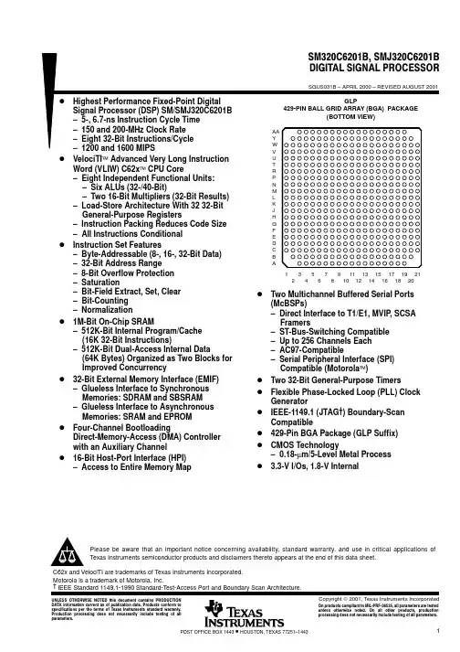
SM320C6201BW14中文资料
- 格式:pdf
- 大小:964.22 KB
- 文档页数:64
元器件交易网
SMJ320C6701 FLOATINGĆPOINT DIGITAL SIGNAL PROCESSOR
SGUS030B – APRIL 2000 – REVISED MAY 2001
D Highest Performance Floating-Point Digital
D
D D D D
D D D
D
D D D D D D
Please be aware that an important notice concerning availability, standard warranty, and use in critical applications of Texas Instruments semiconductor products and disclaimers thereto appears at the end of this data sheet. VelociTI is a trademark of Texas Instruments Incorporated. Motorola is a trademark of Motorola, Inc. † IEEE Standard 1149.1-1990 Standard-Test-Access Port and Boundary Scan Architecture.
Signal Processor (DSP) SMJ320C6701 – 7-, 6-ns Instruction Cycle Time – 140-, 167-MHz Clock Rate – Eight 32-Bit Instructions/Cycle – Up to 1 GFLOPS Performance – Pin-Compatible With ’C6201 Fixed-Point DSP SMJ: QML Processing to MIL-PRF-38535 SM: Standard Processing Operating Temperature Ranges – Extended (W) –55°C to 115°C – Extended (S) –40°C to 90°C VelociTI Advanced Very Long Instruction Word (VLIW) ’C67x CPU Core – Eight Highly Independent Functional Units: – Four ALUs (Floating- and Fixed-Point) – Two ALUs (Fixed-Point) – Two Multipliers (Floating- and Fixed-Point) – Load-Store Architecture With 32 32-Bit General-Purpose Registers – Instruction Packing Reduces Code Size – All Instructions Conditional Instruction Set Features – Hardware Support for IEEE Single-Precision Instructions – Hardware Support for IEEE Double-Precision Instructions – Byte-Addressable (8-, 16-, 32-Bit Data) – 32-Bit Address Range – 8-Bit Overflow Protection – Saturation – Bit-Field Extract, Set, Clear – Bit-Counting – Normalization
D 1M-Bit On-Chip SRAM
– 512K-Bit Internal Program/Cache (16K 32-Bit Instructions) – 512K-Bit Dual-Access Internal Data (64K Bytes) 32-Bit External Memory Interface (EMIF) – Glueless Interface to Synchronous Memories: SDRAM and SBSRAM – Glueless Interface to Asynchronous Memories: SRAM and EPROM Four-Channel Bootloading Direct-Memory-Access (DMA) Controller With an Auxiliary Channel 16-Bit Host-Port Interface (HPI) – Access to Entire Memory Map Two Multichannel Buffered Serial Ports (McBSPs) – Direct Interface to T1/E1, MVIP, SCSA Framers – ST-Bus-Switching Compatible – Up to 256 Channels Each – AC97-Compatible – Serial-Peripheral-Interface (SPI) Compatible (Motorola) Two 32-Bit General-Purpose Timers Flexible Phase-Locked-Loop (PLL) Clock Generator IEEE-1149.1 (JTAG†) Boundary-Scan-Compatible 429-Pin Ceramic Ball Grid Array (CBGA) Package (GLP Suffix) 0.18-µm/5-Level Metal Process – CMOS Technology 3.3-V I/Os, 1.9-V Internal
POST OFFICE BOX 1443
• HOUSTON, TEXAS 77251–1443
1
元器件交易网
SMJ320C6701 FLOATINGĆPOINT DIGITAL SIGNAL PROCESSOR
SGUS030B – APRIL 2000 – REVISED MAY 2001
GLP PACKAGE (BOTTOM VIEW)
AA Y W V U T R P N M L K J H G F E D C B A 1 2 3 4 5 6 7 8 9 10 11 12 13 14 15 16 17 18 19 20 21
description
The SMJ320C67x DSPs are the floating-point DSP family in the SMJ320C6000 platform. The SMJ320C6701 (’C6701) device is based on the high-performance, advanced VelociTI very-long-instruction-word (VLIW) architecture developed by Texas Instruments (TI), making this DSP an excellent choice for multichannel and multifunction applications. With performance of up to 1 giga floating-point operations per second (GFLOPS) at a clock rate of 167 MHz, the ’C6701 offers cost-effective solutions to high-performance DSP programming challenges. The ’C6701 DSP possesses the operational flexibility of high-speed controllers and the numericalrocessor has 32 general-purpose registers of 32-bit word length and eight highly independent functional units. The eight functional units provide four floating-/fixed-point ALUs, two fixed-point ALUs, and two floating-/fixed-point multipliers. The ’C6701 can produce two multiply-accumulates (MACs) per cycle for a total of 334 million MACs per second (MMACS). The ’C6701 DSP also has application-specific hardware logic, on-chip memory, and additional on-chip peripherals. The ’C6701 includes a large bank of on-chip memory and has a powerful and diverse set of peripherals. Program memory consists of a 64K-byte block that is user-configurable as cache or memory-mapped program space. Data memory consists of two 32K-byte blocks of RAM. The peripheral set includes two multichannel buffered serial ports (McBSPs), two general-purpose timers, a host-port interface (HPI), and a glueless external memory interface (EMIF) capable of interfacing to SDRAM or SBSRAM and asynchronous peripherals. The ’C6701 has a complete set of development tools which includes: a new C compiler, an assembly optimizer to simplify programming and scheduling, and a Windows debugger interface for visibility into source code execution.
SMJ320C6701 FLOATINGĆPOINT DIGITAL SIGNAL PROCESSOR
SGUS030B – APRIL 2000 – REVISED MAY 2001
D Highest Performance Floating-Point Digital
D
D D D D
D D D
D
D D D D D D
Please be aware that an important notice concerning availability, standard warranty, and use in critical applications of Texas Instruments semiconductor products and disclaimers thereto appears at the end of this data sheet. VelociTI is a trademark of Texas Instruments Incorporated. Motorola is a trademark of Motorola, Inc. † IEEE Standard 1149.1-1990 Standard-Test-Access Port and Boundary Scan Architecture.
Signal Processor (DSP) SMJ320C6701 – 7-, 6-ns Instruction Cycle Time – 140-, 167-MHz Clock Rate – Eight 32-Bit Instructions/Cycle – Up to 1 GFLOPS Performance – Pin-Compatible With ’C6201 Fixed-Point DSP SMJ: QML Processing to MIL-PRF-38535 SM: Standard Processing Operating Temperature Ranges – Extended (W) –55°C to 115°C – Extended (S) –40°C to 90°C VelociTI Advanced Very Long Instruction Word (VLIW) ’C67x CPU Core – Eight Highly Independent Functional Units: – Four ALUs (Floating- and Fixed-Point) – Two ALUs (Fixed-Point) – Two Multipliers (Floating- and Fixed-Point) – Load-Store Architecture With 32 32-Bit General-Purpose Registers – Instruction Packing Reduces Code Size – All Instructions Conditional Instruction Set Features – Hardware Support for IEEE Single-Precision Instructions – Hardware Support for IEEE Double-Precision Instructions – Byte-Addressable (8-, 16-, 32-Bit Data) – 32-Bit Address Range – 8-Bit Overflow Protection – Saturation – Bit-Field Extract, Set, Clear – Bit-Counting – Normalization
D 1M-Bit On-Chip SRAM
– 512K-Bit Internal Program/Cache (16K 32-Bit Instructions) – 512K-Bit Dual-Access Internal Data (64K Bytes) 32-Bit External Memory Interface (EMIF) – Glueless Interface to Synchronous Memories: SDRAM and SBSRAM – Glueless Interface to Asynchronous Memories: SRAM and EPROM Four-Channel Bootloading Direct-Memory-Access (DMA) Controller With an Auxiliary Channel 16-Bit Host-Port Interface (HPI) – Access to Entire Memory Map Two Multichannel Buffered Serial Ports (McBSPs) – Direct Interface to T1/E1, MVIP, SCSA Framers – ST-Bus-Switching Compatible – Up to 256 Channels Each – AC97-Compatible – Serial-Peripheral-Interface (SPI) Compatible (Motorola) Two 32-Bit General-Purpose Timers Flexible Phase-Locked-Loop (PLL) Clock Generator IEEE-1149.1 (JTAG†) Boundary-Scan-Compatible 429-Pin Ceramic Ball Grid Array (CBGA) Package (GLP Suffix) 0.18-µm/5-Level Metal Process – CMOS Technology 3.3-V I/Os, 1.9-V Internal
POST OFFICE BOX 1443
• HOUSTON, TEXAS 77251–1443
1
元器件交易网
SMJ320C6701 FLOATINGĆPOINT DIGITAL SIGNAL PROCESSOR
SGUS030B – APRIL 2000 – REVISED MAY 2001
GLP PACKAGE (BOTTOM VIEW)
AA Y W V U T R P N M L K J H G F E D C B A 1 2 3 4 5 6 7 8 9 10 11 12 13 14 15 16 17 18 19 20 21
description
The SMJ320C67x DSPs are the floating-point DSP family in the SMJ320C6000 platform. The SMJ320C6701 (’C6701) device is based on the high-performance, advanced VelociTI very-long-instruction-word (VLIW) architecture developed by Texas Instruments (TI), making this DSP an excellent choice for multichannel and multifunction applications. With performance of up to 1 giga floating-point operations per second (GFLOPS) at a clock rate of 167 MHz, the ’C6701 offers cost-effective solutions to high-performance DSP programming challenges. The ’C6701 DSP possesses the operational flexibility of high-speed controllers and the numericalrocessor has 32 general-purpose registers of 32-bit word length and eight highly independent functional units. The eight functional units provide four floating-/fixed-point ALUs, two fixed-point ALUs, and two floating-/fixed-point multipliers. The ’C6701 can produce two multiply-accumulates (MACs) per cycle for a total of 334 million MACs per second (MMACS). The ’C6701 DSP also has application-specific hardware logic, on-chip memory, and additional on-chip peripherals. The ’C6701 includes a large bank of on-chip memory and has a powerful and diverse set of peripherals. Program memory consists of a 64K-byte block that is user-configurable as cache or memory-mapped program space. Data memory consists of two 32K-byte blocks of RAM. The peripheral set includes two multichannel buffered serial ports (McBSPs), two general-purpose timers, a host-port interface (HPI), and a glueless external memory interface (EMIF) capable of interfacing to SDRAM or SBSRAM and asynchronous peripherals. The ’C6701 has a complete set of development tools which includes: a new C compiler, an assembly optimizer to simplify programming and scheduling, and a Windows debugger interface for visibility into source code execution.