
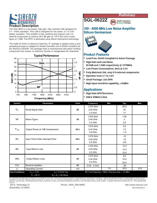
SGL-0622Z_datasheet
- 格式:pdf
- 大小:117.36 KB
- 文档页数:5

© 2007 Microchip Technology Inc.DS21191P-page 124AA128/24LC128/24FC128Device Selection TableFeatures:•Single supply with operation down to 1.7V for 24AA128/24FC128 devices, 2.5V for 24LC128 devices•Low-power CMOS technology:-Write current 3 mA, typical-Standby current 100 nA, typical•2-wire serial interface, I 2C™ compatible •Cascadable up to eight devices•Schmitt Trigger inputs for noise suppression •Output slope control to eliminate ground bounce •100 kHz and 400 kHz clock compatibility • 1 MHz clock for FC versions •Page write time 5 ms, typical •Self-timed erase/write cycle•64-byte page write buffer <adjust per device>•Hardware write-protect •ESD protection >4000V•More than 1 million erase/write cycles •Data retention > 200 years •Factory programming available•Packages include 8-lead PDIP , SOIC, TSSOP , DFN and MSOP packages •Pb-free and RoHS compliant•Temperature ranges:Description:The Microchip Technology Inc. 24AA128/24LC128/24FC128 (24XX128*) is a 16K x 8 (128 Kbit) Serial Electrically Erasable PROM (EEPROM), capable of operation across a broad voltage range (1.7V to 5.5V).It has been developed for advanced, low-power applications such as personal communications or data acquisition. This device also has a page write capabil-ity of up to 64 bytes of data. This device is capable of both random and sequential reads up to the 128K boundary. Functional address lines allow up to eight devices on the same bus, for up to 1Mbit address space. This device is available in the standard 8-pin plastic DIP , SOIC (3.90 mm and 5.28 mm), TSSOP ,MSOP and DFN packages.Block Diagram*24XX128 is used in this document as a generic part number for the 24AA128/24LC128/24FC128 devices.Package TypesPart Number V CC Range Max. Clock Frequency Temp. Ranges24AA128 1.7-5.5V 400kHz (1)I 24LC128 2.5-5.5V 400kHz I, E 24FC128 1.7-5.5V1MHz (2)INote 1:100kHz for V CC < 2.5V.2:400kHz for V CC < 2.5V.-Industrial (I): -40°C to +85°C -Automotive (E): -40°C to +125°CHV GeneratorEEPROM Array Page LatchesYDECXDECSense Amp.R/W ControlM emory C ontrol L ogicI/O C ontrol L ogic I/O A0A1A2SDASCLV CC V SSWPA0A1A2V SSV CC WP SCL SDA1234876524X X 128PDIP/SOICTSSOP/MSOP*A0A1A2V SS12348765V CC WP SCL SDA24X X 128DFNA0A1A2V SSWP SCL SDA24X X 12856784321V CC Note: * Pins A0 and A1 are no-connects for the MSOP package only.128K I 2C ™ CMOS Serial EEPROM24AA128/24LC128/24FC128DS21191P-page 2© 2007 Microchip Technology Inc.1.0ELECTRICAL CHARACTERISTICSAbsolute Maximum Ratings (†)V CC .............................................................................................................................................................................6.5V All inputs and outputs w.r.t. V SS .........................................................................................................-0.6V to V CC +1.0V Storage temperature ...............................................................................................................................-65°C to +150°C Ambient temperature with power applied................................................................................................-40°C to +125°C ESD protection on all pins ......................................................................................................................................................≥4kV TABLE 1-1:DC CHARACTERISTICS† NOTICE : Stresses above those listed under “Absolute Maximum Ratings” may cause permanent damage to the device. This is a stress rating only and functional operation of the device at those or any other conditions above those indicated in the operational listings of this specification is not implied. Exposure to maximum rating conditions for extended periods may affect device reliability.DC CHARACTERISTICS Electrical Characteristics:Industrial (I):V CC = +1.7V to 5.5V T A = -40°C to +85°C Automotive (E):V CC = +2.5V to 5.5V T A = -40°C to 125°CParam.No.Sym.CharacteristicMin.Max.Units ConditionsD1—A0, A1, A2, SCL, SDA and WP pins:————D2V IH High-level input voltage 0.7 V CC—V —D3V IL Low-level input voltage —0.3 V CC 0.2 V CCV V V CC ≥ 2.5V V CC < 2.5V D4V HYS Hysteresis of Schmitt Trigger inputs (SDA, SCL pins)0.05 V CC—V V CC ≥ 2.5V (Note 1)D5V OL Low-level output voltage —0.40V I OL = 3.0mA @ V CC = 4.5V I OL = 2.1mA @ V CC = 2.5V D6I LI Input leakage current —±1μA V IN = V SS or V CC , WP = V SS V IN = V SS or V CC , WP = V CC D7I LO Output leakage current —±1μA V OUT = V SS or V CC D8C IN , C OUT Pin capacitance (all inputs/outputs)—10pF V CC = 5.0V (Note 1)T A = 25°C, F CLK = 1MHz D9I CC Read Operating current—400μA V CC = 5.5V, SCL = 400kHz I CC Write —3mA V CC = 5.5VD10I CCSStandby current—1μAT A = -40°C to +85°CSCL = SDA = V CC = 5.5V A0, A1, A2, WP = V SS —5μAT A = -40°C to 125°CSCL = SDA = V CC = 5.5V A0, A1, A2, WP = V SSNote 1:This parameter is periodically sampled and not 100% tested.24AA128/24LC128/24FC128 TABLE 1-2:AC CHARACTERISTICSAC CHARACTERISTICS Electrical Characteristics:Industrial (I):V CC = +1.7V to 5.5V T A = -40°C to +85°C Automotive (E):V CC = +2.5V to 5.5V T A = -40°C to 125°CParam.No.Sym.Characteristic Min.Max.Units Conditions1F CLK Clock frequency————1004004001000kHz 1.7V ≤ V CC< 2.5V2.5V ≤ V CC≤ 5.5V1.7V ≤ V CC<2.5V 24FC1282.5V ≤ V CC≤ 5.5V 24FC1282T HIGH Clock high time4000600600500————ns 1.7V ≤ V CC< 2.5V2.5V ≤ V CC≤ 5.5V1.7V ≤ V CC<2.5V 24FC1282.5V ≤ V CC≤ 5.5V 24FC1283T LOW Clock low time470013001300500————ns 1.7V ≤ V CC< 2.5V2.5V ≤ V CC≤ 5.5V1.7V ≤ V CC<2.5V 24FC1282.5V ≤ V CC≤ 5.5V 24FC1284T R SDA and SCL rise time(Note1)———1000300300ns 1.7V ≤ V CC< 2.5V2.5V ≤ V CC≤ 5.5V1.7V ≤ V CC≤ 5.5V 24FC1285T F SDA and SCL fall time(Note1)——300100ns All except, 24FC1281.7V ≤ V CC≤ 5.5V 24FC1286T HD:STA Start condition hold time4000600600250————ns 1.7V ≤ V CC< 2.5V2.5V ≤ V CC≤ 5.5V1.7V ≤ V CC<2.5V 24FC1282.5V ≤ V CC≤ 5.5V 24FC1287T SU:STA Start condition setup time4700600600250————ns 1.7V ≤ V CC< 2.5V2.5V ≤ V CC≤ 5.5V1.7V ≤ V CC<2.5V 24FC1282.5V ≤ V CC≤ 5.5V 24FC1288T HD:DAT Data input hold time0—ns(Note2)9T SU:DAT Data input setup time250100100———ns 1.7V ≤ V CC< 2.5V2.5V ≤ V CC≤ 5.5V1.7V ≤ V CC≤ 5.5V 24FC12810T SU:STO Stop condition setup time4000600600250————ns 1.7V ≤ V CC< 2.5V2.5V ≤ V CC≤ 5.5V1.7V ≤ V CC<2.5V 24FC1282.5V ≤ V CC≤ 5.5V 24FC12811T SU:WP WP setup time4000600600———ns 1.7V ≤ V CC< 2.5V2.5V ≤ V CC≤ 5.5V1.7V ≤ V CC≤ 5.5V 24FC12812T HD:WP WP hold time470013001300———ns 1.7V ≤ V CC< 2.5V2.5V ≤ V CC≤ 5.5V1.7V ≤ V CC≤ 5.5V 24FC128Note1:Not 100% tested. C B = total capacitance of one bus line in pF.2:As a transmitter, the device must provide an internal minimum delay time to bridge the undefined region (minimum 300ns) of the falling edge of SCL to avoid unintended generation of Start or Stop conditions.3:The combined T SP and V HYS specifications are due to new Schmitt Trigger inputs, which provide improved noise spike suppression. This eliminates the need for a T I specification for standard operation.4:This parameter is not tested but ensured by characterization. For endurance estimates in a specific application, please consult the Total Endurance™ Model, which can be obtained from Microchip’s web siteat .© 2007 Microchip Technology Inc.DS21191P-page 324AA128/24LC128/24FC128DS21191P-page 4© 2007 Microchip Technology Inc.FIGURE 1-1:BUS TIMING DATA13T AAOutput valid from clock (Note 2)————3500900900400ns1.7V ≤ V CC <2.5V 2.5V ≤ V CC ≤ 5.5V1.7V ≤ V CC <2.5V 24FC1282.5V ≤ V CC ≤ 5.5V 24FC12814T BUFBus free time: Time the bus must be free before a new transmission can start 470013001300500————ns1.7V ≤ V CC <2.5V 2.5V ≤ V CC ≤ 5.5V1.7V ≤ V CC <2.5V 24FC1282.5V ≤ V CC ≤ 5.5V 24FC12815T OF Output fall time from V IH minimum to V IL maximum C B ≤ 100pF10 + 0.1C B250250nsAll except, 24FC128 (Note 1)24FC128 (Note 1)16T SP Input filter spike suppression (SDA and SCL pins)—50ns All except, 24FC128 (Notes 1 and 3)17T WC Write cycle time (byte or page)—5ms—18—Endurance1,000,000—cycles 25°C (Note 4)TABLE 1-2:AC CHARACTERISTICS (CONTINUED)AC CHARACTERISTICS Electrical Characteristics:Industrial (I):V CC = +1.7V to 5.5V T A = -40°C to +85°C Automotive (E):V CC = +2.5V to 5.5V T A = -40°C to 125°CParam.No.Sym.Characteristic Min.Max.Units ConditionsNote 1:Not 100% tested. C B = total capacitance of one bus line in pF.2:As a transmitter, the device must provide an internal minimum delay time to bridge the undefined region (minimum 300ns) of the falling edge of SCL to avoid unintended generation of Start or Stop conditions.3:The combined T SP and V HYS specifications are due to new Schmitt Trigger inputs, which provide improved noise spike suppression. This eliminates the need for a T I specification for standard operation.4:This parameter is not tested but ensured by characterization. For endurance estimates in a specific application, please consult the Total Endurance™ Model, which can be obtained from Microchip’s web site at .(unprotected)(protected)SCL SDA INSDA OUTWP57616328913D441011121424AA128/24LC128/24FC1282.0PIN DESCRIPTIONSThe descriptions of the pins are listed in Table2-1.TABLE 2-1:PIN FUNCTION TABLE2.1A0, A1, A2 Chip Address Inputs The A0, A1 and A2 inputs are used by the 24XX128 for multiple device operations. The levels on these inputs are compared with the corresponding bits in the slave address. The chip is selected if the compare is true. For the MSOP package only, pins A0 and A1 are not connected.Up to eight devices (two for the MSOP package) may be connected to the same bus by using different Chip Select bit combinations. These inputs must be connected to either V CC or V SS.In most applications, the chip address inputs A0, A1 and A2 are hard-wired to logic ‘0’ or logic ‘1’. For applications in which these pins are controlled by a microcontroller or other programmable device, the chip address pins must be driven to logic ‘0’ or logic ‘1’before normal device operation can proceed.2.2Serial Data (SDA)This is a bidirectional pin used to transfer addresses and data into and out of the device. It is an open drain terminal. Therefore, the SDA bus requires a pull-up resistor to V CC (typical 10kΩ for 100kHz, 2kΩ for 400kHz and1MHz).For normal data transfer, SDA is allowed to change only during SCL low. Changes during SCL high are reserved for indicating the Start and Stop conditions.2.3Serial Clock (SCL)This input is used to synchronize the data transfer to and from the device.2.4Write-Protect (WP)This pin must be connected to either V SS or V CC. If tied to V SS, write operations are enabled. If tied to V CC, write operations are inhibited but read operations are not affected.3.0FUNCTIONAL DESCRIPTION The 24XX128 supports a bidirectional 2-wire bus and data transmission protocol. A device that sends data onto the bus is defined as a transmitter and a device receiving data as a receiver. The bus must be controlled by a master device which generates the Serial Clock (SCL), controls the bus access and generates the Start and Stop conditions while the 24XX128 works as a slave. Both master and slave can operate as a transmitter or receiver, but the master device determines which mode is activated.Name 8-pinPDIP8-pinSOIC8-pinTSSOP8-pinMSOP8-pinDFNFunctionA0111—1User Configurable Chip SelectA1222—2User Configurable Chip Select (NC)———1, 2—Not ConnectedA233333User Configurable Chip SelectV SS44444GroundSDA55555Serial DataSCL66666Serial Clock(NC)—————Not ConnectedWP77777Write-Protect InputV CC88888+1.7V to 5.5V (24AA128)+2.5V to 5.5V (24LC128)+1.7V to 5.5V (24FC128)© 2007 Microchip Technology Inc.DS21191P-page 524AA128/24LC128/24FC128DS21191P-page 6© 2007 Microchip Technology Inc.4.0BUS CHARACTERISTICSThe following bus protocol has been defined:•Data transfer may be initiated only when the bus is not busy.•During data transfer, the data line must remain stable whenever the clock line is high. Changes in the data line while the clock line is high will be interpreted as a Start or Stop condition.Accordingly, the following bus conditions have been defined (Figure 4-1).4.1Bus Not Busy (A)Both data and clock lines remain high.4.2Start Data Transfer (B)A high-to-low transition of the SDA line while the clock (SCL) is high determines a Start condition. All commands must be preceded by a Start condition.4.3Stop Data Transfer (C)A low-to-high transition of the SDA line, while the clock (SCL) is high, determines a Stop condition. All operations must end with a Stop condition.4.4Data Valid (D)The state of the data line represents valid data when,after a Start condition, the data line is stable for the duration of the high period of the clock signal.The data on the line must be changed during the low period of the clock signal. There is one bit of data per clock pulse.Each data transfer is initiated with a Start condition and terminated with a Stop condition. The number of the data bytes transferred between the Start and Stop conditions is determined by the master device.4.5AcknowledgeEach receiving device, when addressed, is obliged to generate an Acknowledge signal after the reception of each byte. The master device must generate an extra clock pulse, which is associated with this Acknowledge bit.A device that acknowledges must pull down the SDA line during the acknowledge clock pulse in such a way that the SDA line is stable low during the high period of the acknowledge related clock pulse. Of course, setup and hold times must be taken into account. During reads, a master must signal an end of data to the slave by NOT generating an Acknowledge bit on the last byte that has been clocked out of the slave. In this case, the slave (24XX128) will leave the data line high to enable the master to generate the Stop condition.FIGURE 4-1:DATA TRANSFER SEQUENCE ON THE SERIAL BUSNote:The 24XX128 does not generate any Acknowledge bits if an internal programming cycle is in progress.Address or AcknowledgeValid Data Allowed to ChangeStop ConditionStart ConditionSCLSDA(A)(B)(D)(D)(C)(A)© 2007 Microchip Technology Inc.DS21191P-page 724AA128/24LC128/24FC1285.0DEVICE ADDRESSINGA control byte is the first byte received following the Start condition from the master device (Figure 5-1).The control byte consists of a 4-bit control code. For the 24XX128, this is set as ‘1010’ binary for read and write operations. The next three bits of the control byte are the Chip Select bits (A2, A1, A0). The Chip Select bits allow the use of up to eight 24XX128 devices on the same bus and are used to select which device is accessed. The Chip Select bits in the control byte must correspond to the logic levels on the corresponding A2,A1 and A0 pins for the device to respond. These bits are, in effect, the three Most Significant bits of the word address.For the MSOP package, the A0 and A1 pins are not connected. During device addressing, the A0 and A1Chip Select bits (Figures 5-1 and 5-2) should be set to ‘0’. Only two 24XX128 MSOP packages can be connected to the same bus.The last bit of the control byte defines the operation to be performed. When set to a one, a read operation is selected. When set to a zero, a write operation is selected. The next two bytes received define the address of the first data byte (Figure 5-2). Because only A13…A0 are used, the upper two address bits are “don’t care” bits. The upper address bits are transferred first, followed by the Less Significant bits.Following the Start condition, the 24XX128 monitors the SDA bus checking the device type identifier being transmitted. Upon receiving a ‘1010’ code and appropriate device select bits, the slave device outputs an Acknowledge signal on the SDA line. Depending on the state of the R/W bit, the 24XX128 will select a read or write operation.FIGURE 5-1:CONTROL BYTE FORMAT5.1Contiguous Addressing Across Multiple DevicesThe Chip Select bits A2, A1 and A0 can be used to expand the contiguous address space for up to 1Mbit by adding up to eight 24XX128 devices on the same bus. In this case, software can use A0 of the control byte as address bit A14; A1 as address bit A15; and A2as address bit A16. It is not possible to sequentially read across device boundaries.For the MSOP package, up to two 24XX128 devices can be added for up to 256Kbit of address space. In this case, software can use A2 of the control byte as address bit A16. Bits A0 (A14) and A1 (A15) of the control byte must always be set to logic ‘0’ for the MSOP .FIGURE 5-2:ADDRESS SEQUENCE BIT ASSIGNMENTS11A2A1A0SACKR/W Control CodeChip SelectBits Slave AddressAcknowledge BitStart BitRead/Write Bit 1010A 2A 1A0R/Wx xA 11A 10A 9A 7A 0A 8••••••A 12Control ByteAddress High ByteAddress Low ByteControl CodeChip Select Bitsx = “don’t care” bitA 1324AA128/24LC128/24FC128DS21191P-page 8© 2007 Microchip Technology Inc.6.0WRITE OPERATIONS6.1Byte WriteFollowing the Start condition from the master, the control code (four bits), the Chip Select (three bits) and bus by the master transmitter. This indicates to the addressed slave receiver that the address high byte will follow after it has generated an Acknowledge bit during the ninth clock cycle. Therefore, the next byte transmitted by the master is the high-order byte of the word address and will be written into the Address Pointer of the 24XX128. The next byte is the Least Significant Address Byte. After receiving another Acknowledge signal from the 24XX128, the master device will transmit the data word to be written into the addressed memory location. The 24XX128 acknowl-edges again and the master generates a Stop condition. This initiates the internal write cycle and during this time, the 24XX128 will not generate Acknowledge signals (Figure 6-1). If an attempt is made to write to the array with the WP pin held high, the device will acknowledge the command, but no write cycle will occur, no data will be written, and the device will immediately accept a new command. After a byte Write command, the internal address counter will point to the address location following the one that was just written.6.2Page WriteThe write control byte, word address, and the first data byte are transmitted to the 24XX128 in much the same way as in a byte write. The exception is that instead of generating a Stop condition, the master transmits up to 63 additional bytes, which are temporarily stored in the on-chip page buffer, and will be written into memory once the master has transmitted a Stop condition.Upon receipt of each word, the six lower Address Pointer bits are internally incremented by ‘1’. If themaster should transmit more than 64 bytes prior to generating the Stop condition, the address counter will roll over and the previously received data will be over-written. As with the byte write operation, once the Stop condition is received, an internal write cycle will begin (Figure 6-2). If an attempt is made to write to the array with the WP pin held high, the device will acknowledge the command, but no write cycle will occur, no data will be written and the device will immediately accept a new command.6.3Write ProtectionThe WP pin allows the user to write-protect the entire array (0000-3FFF) when the pin is tied to V CC . If tied to V SS the write protection is disabled. The WP pin is sampled at the Stop bit for every Write command (Figure 1-1). Toggling the WP pin after the Stop bit will have no effect on the execution of the write cycle. FIGURE 6-1:BYTE WRITEFIGURE 6-2:PAGE WRITENote:Page write operations are limited to writing bytes within a single physical page, regardless of the number of bytes actually being written. Physical page boundaries start at addresses that are integer multiples of the page buffer size (or ‘page size’) and end at addresses that are integer multiples of [page size – 1]. If a Page Write command attempts to write across a physical page boundary, the result is that the data wraps around to the beginning of the current page (over-writing data previously stored there),instead of being written to the next page, as might be expected. It is,therefore, necessary for the applica-tion software to prevent page write operations that would attempt to cross a page boundary.x x Bus Activity Master SDA Line Bus ActivityS T A R TControl Byte Address High ByteAddress Low ByteDataS T O P A C KA C KAC K A C Kx = “don’t care” bitS 10100A 2A 1A 0Px x Bus Activity Master SDA Line Bus ActivityS T A R TControl Byte Address High ByteAddress Low ByteData Byte 0S T O P A C KA C KA C K A C KData Byte 63A C Kx = “don’t care” bitS 10100A 2A 1A0P24AA128/24LC128/24FC1287.0ACKNOWLEDGE POLLING Since the device will not acknowledge during a write cycle, this can be used to determine when the cycle is complete (This feature can be used to maximize bus throughput). Once the Stop condition for a Write command has been issued from the master, the device initiates the internally timed write cycle. ACK polling can be initiated immediately. This involves the master sending a Start condition, followed by the control byte0). If the device is still busy with the write cycle, then no ACK will be returned. If no ACK is returned, the Start bit and control byte must be resent. If the cycle is complete, then the device will return the ACK and the master can then proceed with the next Read or Write command. See Figure7-1 for flow diagram.FIGURE 7-1:ACKNOWLEDGEPOLLING FLOWSendWrite CommandSend StopCondition toInitiate Write CycleSend StartSend Control Bytewith R/W = 0Did DeviceAcknowledge(ACK = 0)?NextOperationNoYes© 2007 Microchip Technology Inc.DS21191P-page 924AA128/24LC128/24FC128DS21191P-page 10© 2007 Microchip Technology Inc.8.0READ OPERATIONRead operations are initiated in much the same way as write operations with the exception that the R/W bit of the control byte is set to ‘1’. There are three basic types of read operations: current address read, random read and sequential read.8.1Current Address ReadThe 24XX128 contains an address counter that main-tains the address of the last word accessed, internally incremented by ‘1’. Therefore, if the previous read access was to address ‘n ’ (n is any legal address), the next current address read operation would access data from address n + 1.Upon receipt of the control byte with R/W bit set to ‘1’,the 24XX128 issues an acknowledge and transmits the 8-bit data word. The master will not acknowledge the transfer, but does generate a Stop condition and the 24XX128 discontinues transmission (Figure 8-1).FIGURE 8-1:CURRENT ADDRESS READ8.2Random ReadRandom read operations allow the master to access any memory location in a random manner. To perform this type of read operation, the word address must first be set. This is done by sending the word address to the 24XX128 as part of a write operation (R/W bit set to ‘0’). Once the word address is sent, the master gener-ates a Start condition following the acknowledge. This terminates the write operation, but not before the inter-nal Address Pointer is set. The master then issues the 1’. The 24XX128 will then issue an acknowledge and transmit the 8-bit data word. The master will not acknowledge the transfer but does generate a Stop condition, which causes the 24XX128 to discontinue transmission (Figure 8-2). After a random Read command, the internal address counter will point to the address location following the one that was just read.8.3Sequential ReadSequential reads are initiated in the same way as a random read except that after the 24XX128 transmits the first data byte, the master issues an acknowledge as opposed to the Stop condition used in a random read. This acknowledge directs the 24XX128 to transmit the next sequentially addressed 8-bit word (Figure 8-3). Following the final byte transmitted to the master, the master will NOT generate an acknowledge but will generate a Stop condition. To provide sequential reads, the 24XX128 contains an internal Address Pointer which is incremented by one at the completion of each operation. This Address Pointer allows the entire memory contents to be serially read during one operation. The internal Address Pointer will automatically roll over from address 3FFF to address 0000 if the master acknowledges the byte received from the array address 3FFF.FIGURE 8-2:RANDOM READFIGURE 8-3:SEQUENTIAL READBus Activity Master SDA Line Bus ActivityPS S T O P Control ByteS T A R TData A C KN O A C K1100A A A 1Byte210x xBus Activity MasterSDA Line Bus ActivityA C KN O A C KA C KA C KA C KS T O P S T A R TControl ByteAddress High ByteAddress Low ByteControl ByteData ByteS T A R Tx = “don’t care” bitS 1010A A A 0210S 1010A A A 1210P Bus Activity Master SDA Line Bus ActivityControl ByteData (n)Data (n + 1)Data (n + 2)Data (n + x )N O A C KA C KA C KA C KA C KS T O P P分销商库存信息: PARALLAX602-20012。

Technical Data Sheet Product 243Worldwide Version, October 1995NOT FOR PRODUCT SPECIFICATIONS.THE TECHNICAL DATA CONTAINED HEREIN ARE INTENDED AS REFERENCE ONLY.PLEASE CONTACT LOCTITE CORPORATION QUALITY DEPARTMENT FOR ASSISTANCE AND RECOMMENDATIONS ON SPECIFICATIONS FOR THIS PRODUCT.ROCKY HILL, CT FAX: +1 (860)-571-5473 DUBLIN, IRELAND FAX: +353-(1)-451 - 9959PRODUCT DESCRIPTIONLOCTITE ® Product 243 is a single component anaerobic threadlocking material, which is thixotropic and develops medium strength. The product cures when confined in theabsence of air between close fitting metal surfaces and is particularly suitable for less active substrates such as stainless steel and plated surfaces.TYPICAL APPLICATIONSPrevents loosening and leakage of threaded fasteners.Particularly suitable for applications such as pump or motor mounting bolts, engine rocker nuts or equipment housing screws, where disassembly with hand tools is required for servicing.PROPERTIES OF UNCURED MATERIALTypicalValueRangeChemical Type Dimethacrylate EsterAppearanceOpaque Blue Fluorescent LiquidSpecific Gravity @ 25°C1.08Viscosity @ 25°C, mPa.s (cP) Brookfield RVT***************12,0006,000 to 18,000 @ 20 rpm2,2501,500 to 3,000 DIN 54453, MVD = 129 s -1 after t=180secs 350250 to 500Flash Point (TCC), °C>93TYPICAL CURING PERFORMANCECure speed vs. substrateThe rate of cure will depend on substrate used. The graph below shows the breakaway strength developed with time on M10 steel nuts and bolts compared to different materials and tested according to IS0 10964.S te elZ i nc Di c hr om at eS t ai n l es s S t ee lB r a s s5min 10min30min 1hr3hr6hr24hr72hrCure Time, Hours255075100% o f F u l l S t r e n g t h o n S t e e lCure speed vs. bond gapThe rate of cure will depend on the bondline gap. Gaps in threaded fasteners depend on thread type, quality and size.The following graph shows shear strength developed with time on steel pins and collars at different controlled gaps and tested according to ISO 10123.5min 10min 30min 1hr3hr 6hr 24hr 72hrCure Time, Hours255075100% o f F u l l S t r e n g t h o n S t e e l0.15m m0.05m m0.25m mCure speed vs. temperatureThe rate of cure will depend on the ambient temperature.Graph below shows the breakaway strength developed with time at different temperatures on M10 steel nuts and bolts and tested according to IS0 10964.5min 10min 30min 1hr3hr 6hr 24hr 72hrCure Time, Hours255075100% o f F u l l S t r e n g t h o n S t e e l22°C40°C5 °CCure speed vs. activatorWhere cure speed is unacceptably long, or large gaps are present, applying activator to the surface will improve cure speed. The graph below shows breakaway strength developed with time using ACTIVATOR N and T on M10 Zinc Dichromate steel nuts & bolts and tested according to IS010964.5min 10min30min 1hr3hr6hr24hr72hrCure Time, Hours255075100% o f F u l l S t r e n g t h o n S t e e lAct. TN oA c t i v a t o r A c t NTYPICAL PROPERTIES OF CURED MATERIAL Physical PropertiesCoefficient of thermal expansion, ASTM D696, K -180 x10-6Coefficient of thermal conductivity, ASTM C177, W.m -1 K -10.1Specific Heat , kJ.kg -1 K -10.3Loctite UK Limited, Watchmead,Welwyn Garden City, Herts, AL7 1JB Technical Services Tel: (01707) 358888Customer Services Tel: (01707) 358844TDS 243 October 1995Loctite is a Registered Trademark of Loctite Corporation, Hartford, CT 06106PERFORMANCE OF CURED MATERIAL(After 24 hr at 22°C on M10 steel nuts & bolts)TypicalValue Range Breakaway Torque, IS0 10964 (4.3), N.m 2015 to 25 (lb.in)(180)(130 to 220)Prevail Torque, IS0 10964 (4.5) , N.m 7 4 to 10 (lb.in)(62)(35 to 88)Breakloose Torque, DIN 54454, N.m 2414 to 34 (lb.in)(210)(120 to 300)Max. Prevail Torque, DIN 54454, N.m 2414 to 34 (lb.in)(210)(120 to 300)TYPICAL ENVIRONMENTAL RESISTANCE Test Procedure :Breakloose Torque, DIN 54454Substrate:M10 Zinc Phosphate Nuts&Bolts Cure procedure: 1 week at 22°C Hot StrengthTested at temperature.050100150255075100% R T S t r e n g t hTemperature, °CHeat AgeingAged at temperature indicated and tested at 22°C.01,0002,0003,0004,0005,0000255075100125Hours% I n i t i a l S t r e n g t h , a t R T120°C150°C100°C Chemical / Solvent ResistanceAged under conditions indicated and tested at 22°C.SolventTemp.% Initial Strength retained at100 hr 500 hr 1000 hr 5000 hr Motor Oil125°C 95959595Leaded Petrol 22°C 1001009595Brake Fluid22°C 100100100100Water/Glycol (50%/50%)87°C 95808080Ethanol 22°C 100858585Acetone22°C1001008585GENERAL INFORMATIONThis product is not recommended for use in pure oxygen and/or oxygen rich systems and should not be selected as a sealant for chlorine or other strong oxidising materials.For safe handling information on this product, consult the Material Safety Data Sheet, (MSDS).Where aqueous washing systems are used to clean the surfaces before bonding, it is important to check for compatibility of the washing solution with the adhesive. In some cases these aqueous washes can affect the cure and performance of the adhesive.This product is not normally recommended for use on plastics (particularly thermoplastic materials where stress cracking of the plastic could result). Users are recommended to confirm compatibility of the product with such substrates.Directions for useFor best performance surfaces should be clean and free of grease. Product should be applied to the bolt in sufficient quantity to fill all engaged threads. This product performs best in thin bond gaps, (0.05mm). Very large thread sizes may create large gaps which will affect cure speed and strength.This product is designed to give controlled friction,(torque/tension ratio), during assembly. In critical tightening applications this ratio should be confirmed.StorageProduct shall be ideally stored in a cool, dry location in unopened containers at a temperature between 8°C to 28°C (46°F to 82°F) unless otherwise labelled. Optimal storage is at the lower half of this temperature range. To prevent contamination of unused product, do not return any material to its original container. For further specific shelf life information,contact your local Technical Service Centre.Data RangesThe data contained herein may be reported as a typical value and/or range (based on the mean value ±2 standard deviations). Values are based on actual test data and are verified on a periodic basis.NoteThe data contained herein are furnished for information only and are believed to be reliable. We cannot assume responsibility for the results obtained by others over whose methods we have no control. It is the user's responsibility to determine suitability for the user's purpose of any production methods mentioned herein and to adopt such precautions as may be advisable for the protection of property and of persons against any hazards that may be involved in the handling and use thereof. In light of the foregoing, Loctite Corporation specifically disclaims all warranties expressed or implied,including warranties of merchantability or fitness for a particular purpose, arising from sale or use of Loctite Corporation’s products. Loctite Corporation specifically disclaims any liability for consequential or incidental damages of any kind, including lost profits. The discussion herein of various processes or compositions is not to be interpreted as representation that they are free from domination of patents owned by others or as a licence under any Loctite Corporation patents that may cover such processes or compositions. We recommend that each prospective user test his proposed application before repetitive use, using this data as a guide.This product may be covered by one or more United States or foreign patents or patent applications.。

with High Power Factor and Low-Ripple Current1.0 Features●All-in-one non-dimmable low-cost off-line LED driver(isolated and non-isolated applications)●Supports universal input voltage range (90V AC to 277V AC)and output power up to 45W●Supports flyback/buck-boost or buck topologies●High power factor (PF) with low current-ripple controltechnology●User-configurable power factor setting (> 0.7 to > 0.95)●Able to achieve low THD (< 20%)●User-configurable internal or external over-temperatureprotection (OTP) with temperature-current derating●Tight LED current regulation (±5%) across line and load,and within primary inductance tolerance (±20%)●Isolated design without opto-coupler●Stabilized LED current-ripple control without visibleshimmer or flicker●Active start-up scheme enables fastest possible start-up ●72kHz/90kHz nominal PWM switching frequency withquasi-resonant operation●EZ-EMI® design enhances manufacturability●Built-in single-point fault protection features: LED open-/short-circuit protection and over-current protection●No audible noise over entire operating range 2.0 DescriptionThe iW3622 is a high performance, single-stage AC/DC power controller for LED luminaires with power factor (PF) correction. The device uses digital control technology to build unique control in PWM flyback/buck-boost or buck power supplies to achieve high power factor while minimizing the LED current ripple. This distinctive control approach enables the capability for users to make trade-offs between the PF and LED current ripple in a single-stage design. It can achieve excellent LED current regulation over line and load variation, without the need for secondary feedback circuit. The built-in temperature sensor along with control logic can automatically adjust output current in real-time without visible flicker during the process. Alternatively, the external NTC thermistor is placed close to the hot spots in a design to provide thermal protection in the similar pattern by derating LED current. The iW3622 operates in quasi-resonant mode to provide high efficiency along with a number of key built-in protection features while minimizing the external component count, simplifying EMI design, and lowering the total bill of material cost. It also eliminates the need for loop compensation components while maintaining stability over all operating conditions.Dialog’s innovative proprietary technology maximizes the iW3622 performance in a tiny SOT-23 package. The iW3622 offers two multi-function pins allowing users to configure PF and LED current derating as required with no cost or size impact, thereby providing design flexibility. In addition to providing the temperature sensing via an NTC resistor, the Multi pin also enables active start-up scheme to achieve the shortest possible start-up time without sacrificing active efficiency.3.0 Applications●Solid-state LED lighting●LED lighting ballastwith High Power Factor and Low-Ripple CurrentFigure 3.1: iW3622 Typical Application Circuit (Non-Isolated Buck-Boost Application)OUT +OUTOUT-OUT+Figure 3.2: iW3622 Typical Application Circuit (Isolated Flyback Application)with High Power Factor and Low-Ripple CurrentFigure 3.3: iW3622 Typical Application Circuit (Isolated Flyback Application without Using Active Start-up Device)OUT V OUT+Figure 3.4: iW3622 Typical Application Circuit (Non-Isolated Buck Application)OUT +V OUTwith High Power Factor and Low-Ripple Current4.0 Pinout Description5.0 Absolute Maximum RatingsAbsolute maximum ratings are the parameter values or ranges which can cause permanent damage if exceeded.with High Power Factor and Low-Ripple Current 6.0 Electrical CharacteristicsV CC = 12V, -40°C ≤ T A ≤ 85°C, unless otherwise specifiedwith High Power Factor and Low-Ripple Current Notes:Note 1: These parameters are not 100% tested, and they are guaranteed by design and characterization. Refer to Section9.0 for operation details.Note 2: Two nominal switching frequencies are selectable by product options. They could vary based on the operatingconditions. For further information, refer to Section 9.8.V CC = 12V, -40°C ≤ T A ≤ 85°C, unless otherwise specified Electrical Characteristics (cont.)with High Power Factor and Low-Ripple Current 7.0 Typical Performance CharacteristicsFigure 7.1 : V CC UVLO vs. TemperatureFigure 7.2 : Start-Up Threshold vs. TemperatureFigure 7.3 : Switching Frequency vs. Temperature2Figure 7.4 : Internal Reference vs. Temperature606468727680M a x i m u m f s w (k H z )Ambient Temperature (ºC)1.9901.9941.9982.0022.0062.010I n t e r n a l R e f e r e n c e V o l t a g e (V )Ambient Temperature (ºC)4.404.324.244.164.084.003.923.843.763.683.60-50-25255075100125150V C C U V L O (V )Ambient Temperature (ºC)TBD0.06.03.09.0V CC (V)V C C S u p p l y S t a r t -u p C u r r e n t (µA )Figure 7.5 : V CC vs. V CC Supply Start-up CurrentNotes:Note 1. Operating frequency varies based on the operating conditions; see Section 9.8 for more details.11.1011.0811.0611.0411.0211.0010.9810.9610.9410.9210.9075-50-252550100125150V C C S t a r t -u p T h r e s h o l d (V )Ambient Temperature (ºC)TBD1051041031021011009998979695-50-250255075100125150I O T P (µA )Ambient Temperature (ºC)TBDFigure 7.6 : I OTP vs. Temperaturewith High Power Factor and Low-Ripple Current 8.0 Functional Block DiagramOUTPUTV CCFB/OTP MultiCS/PF Figure 8.1: iW3622 Functional Block Diagramwith High Power Factor and Low-Ripple Current 9.1 Pin DetailPin 1 – V CCPower supply for the controller during normal operation. The controller starts up when V CC reaches 15.0V (typical) and shuts down when the V CC voltage drops below 6.5V (typical) respectively. A decoupling capacitor of 0.1μF or so should be connected between the V CC pin and GND. Pin 2 – FB/OTPUsed to configure OTP setting at the beginning of start-up, and sense output via auxiliary winding during normal operation for output regulation.Pin 3 – MultiMulti-function pin. This signal is pulled low after start-up is partially finished to cut off the active device. In the meantime, an internal current source of 100μA flows out of this pin to pass through an external NTC resistor to sense the ambient temperature, thus providing an over-temperature power derating function.Pin 4 – CS/PFUsed to configure PF setting at the beginning of start-up, and sense primary current during normal operation for cycle-by-cycle peak current control and limit.Pin 5 – GND Ground.Pin 6 – OUTPUTGate drive for the external power FET switch9.2 Active Start-up and AdaptivelyControlled Soft-Start The iW3622 features a proprietary soft-start scheme to achieve fast build-up of output voltage and smooth ramp-up of LED current for a variety of output conditions including output voltage up to 100V above. In addition, the active start-up scheme enables shortest possible turn-on delay without sacrificing operating efficiency. Refer to Figure 8.1 for the block diagram and Figure 3.2 for the active start-up circuit using external depletion NFET. Prior to start-up, the ENABLE signal is low, and the Multi pin voltage closely follows the V CC pin voltage, as shown 9.0 Theory of OperationThe iW3622 is a digital power controller dedicated for single-stage off-line LED driver with power factor correction. The device uses a new, proprietary primary-side control technology to eliminate the opto-isolated feedback and secondary regulation circuits required in traditional designs. This results in a low-cost small-size solution for LED lighting applications. The iW3622 uses a unique control approach in PWM flyback/buck-boost or buck power supplies to achieve high power factor meanwhile minimizing LED current ripple. Furthermore, Dialog’s digital control technology enables tight output current regulation, user-programmability to allow for making trade-offs between PF and LED current ripple, as well as full-featured circuit protection with primary-side control.Referring to the block diagram in Figure 8.1, the iW3622 has CS/PF and FB/OTP pins for two-fold functions. At the beginning of start-up, a fixed current source flows out of the two pins alternatively, generating voltage levels proportional to resistance values from the pins to GND, which are then identified by the controller to set the requirement for PF and OTP respectively. During normal operation, the digital logic control block generates the switching on-time and off-time information based on the output voltage and current feedback signal and provides commands to control the external MOSFET. The CS/PF is an analog input configured to sense the primary current in a voltage form. In order to achieve the peak current mode control and cycle-by-cycle current limit, the V IPK sets the threshold for the CS/PF to compare with, and it varies in the range of 0.25V (typical) to 1.00V (typical) under different line and load conditions. With intelligent control approach, the iW3622 realizes high power factor correction with minimal output current ripple.The iW3622 operates in quasi-resonant mode to providehigh efficiency and simplify EMI design. In addition, the iW3622 incorporates a number of key built-in protectionfeatures, including LED short-circuit and open protections,over-current protection, and moreover, a distinctivetemperature-current derating function in an attempt to maximize LED current under safe operating condition before initiating thermal shutdown. Using Dialog’s state-of-the-art primary-feedback technology, the iW3622 removes the need for secondary feedback circuit while achieving excellent line and load regulation. Furthermore, the iW3622 eliminates the need for loop compensation components while maintainingstability over all operating conditions.with High Power Factor and Low-Ripple Currentin Figure 9.1. Consequently, the depletion NFET is turned on, allowing the start-up current to charge the V CC bypass capacitor. When the V CC bypass capacitor is charged to a voltage higher than the start-up threshold V CC(ST), the ENABLE signal becomes active and the iW3622 begins to perform PF and OTP configurations (See Section 9.3) followed by initial OTP check (See Section 9.13 and 9.14). Afterwards, the iW3622 commences soft-start function. The whole soft-start process can break down into several stages based on the output voltage levels, which is indirectly sensed by FB/OTP signal at the primary side. At different stages, the iW3622 adaptively controls the switching frequency and primary-side peak current such that the output voltage can always build up very fast at the early stages before LEDs light up, and smoothly transition to the desired regulation current level, meanwhile meeting the power factor requirement at steady-state operation. In the iW3622, the transition can be selected to happen early or late by product options. For designs supporting wide range of output voltage, the transition needs to happen early in order to avoid LED current overshoot for applications with low output voltage. Otherwise, the transition can be set to happen late in order to speed up start-up.V CCENABLEStart-up SequencingV OUTS 1S 2Multi1. PF Configuration2. OTP Configuration3. Initial OTP CheckFigure 9.1: Start-up Sequencing DiagramIn the iW3622, at the transition point, the switch S 1 is turned on to cut off the depletion NFET, thus eliminating the start-up resistors power consumption during normal operation. After a few clocks delay, S 2 is turned on to allow for the internal 100μA current source to flow out of the Multi pin to generate a corresponding voltage on the NTC resistor.If at any time the V CC voltage drops below under voltage lockout (UVLO) threshold V CC(UVL) then the iW3622 goes to shutdown. At this time ENABLE signal becomes low, and the V CC capacitor begins to charge up again towards the start-up threshold to initiate a new soft-start process.In applications where the active start-up is not needed, the start-up resistor can be directly connected to the V CC pin without using the active start-up device, and the Multi pin can be left unconnected. Refer to Figure 3.3 for the application circuit.9.3 PF and OTP ConfigurationsThe iW3622 incorporates an innovative approach to allow users to configure PF and OTP current derating selections externally. In the iW3622, power factor can be set to four levels externally in order to trade off with LED current ripple, as shown in Table 9.1. In addition, for the over-temperature protection, depending on whether it is internal or external, either the temperature at which the device starts to derate LED current or the derating step-size can also be set at the configuration stage.OUT +OUTThe configurations of PF and OTP derating are only performed once after the ENABLE signal becomes active, and completed before the soft-start commences. Theconfigurations involve CS/PF and FB/OTP pins and someresistors connected to the pins. Figure 9.2 shows theschematic highlighting the resistors used for configurations.During PF configuration, the iW3622 does not send out anydrive signal at OUTPUT pin, and the switch Q1 remains in off-state. A fixed current flows out of CS/PF pin, which generates a voltage proportional to the resistance value ofFigure 9.2: Typical Application Circuit HighlightingConfiguration Resistorswith High Power Factor and Low-Ripple CurrentR PF and R CS(in series). The internal digital control block identifies the resistance value between CS/PF pin to ground, and then sets the control algorithm accordingly. Table 9.1 lists the resistance range of R PF for configuring four-level of PF.In applications, the selection of R PF and R CS is straight-forward. R CS is usually small and its resistance is negligible compared to R PF in determining PF level during configuration. However, it directly sets output current, whereas R PF does not play a role (See Section 9.5). Therefore, the values of R PF and R CS can be determined separately.Following the completion of configuring PF, the iW3622 enters the stage of configuring OTP derating selection. During this stage, switch Q1 still remains in off-state, and the fixed current flows out of FB/OTP pin and generates a voltage proportional to the paralleled resistance of R1 and R2, since the bias winding is virtually shorted. Consequently, the paralleled resistance of R1 and R2 is identified and used to set the OTP derating levels. Meanwhile, during normal operation, the FB/OTP pin reflects output voltage in real-time. The ratio of R1 to R2 sets nominal output voltage, which represents the voltage level the iW3622 attempts to regulate to during constant voltage operation. Based on the two equations, R1 and R2 can be readily derived.The iW3622 provides 3-level OTP derating selections. Table 9.2 lists the resistance range of paralleled R1 and R2 for each configuration level. Note, the OTP level has different meaning for the external NTC-based and internal junction-based OTP derating. For the NTC-based OTP derating, the OTP level corresponds to different step-size of OTP derating. For the internal-based OTP derating, it corresponds to the temperature at which the iW3622 starts to derate output current.In practice, for both PF and OTP configurations, it is recommended that the resistance be selected in the middle of the range where possible.After completing PF and OTP configurations, the iW3622 will perform an initial OTP check, and it will initiate a soft-start process if the junction temperature is below 130°C (typical) for product options with internal OTP protection, or the Multi pin voltage is above 0.84V for product options with external OTP protection.9.4 Understanding Primary Feedback Figure 9.3 illustrates a simplified flyback converter. When the switch Q1 conducts during t ON(t), the current i g(t) is directly drawn from rectified sinusoid v g(t). The energy E g(t) is stored in the magnetizing inductance L M. The rectifying diode D1 is reverse biased and the load current I O is supplied by thePF Level123 4R PF Range* (kΩ)0 - 0.88 1.36 – 3.00 3.87 – 5.60 6.95 – 20Resulting PF**> 0.9> 0.95> 0.7< 0.7* R CS is usually very small (a few Ohms), and can be neglected compared to R PF in consideration.** The data are from typical designs. Level 4 is intended to mitigate LED line ripple with big input bulk capacitance.Table 9.1: Recommended resistance range to set power factor (PF) levelOTP Level123Paralleled R1 and R2 Range (k W) 1.80 – 2.25 2.97 – 3.78 4.78 – 20NTC OTP Derating Derating Step-Size5%7.5%10%Internal OTP Derating The temperature at which the iW3622starts to derate output current100 °C110 °C120 °CTable 9.2: Recommended resistance range to over-temperature protection (OTP) selectionwith High Power Factor and Low-Ripple Currentsecondary capacitor C O . When Q1 turns off, D1 conducts and the stored energy E g (t) is delivered to the output.v OFigure 9.3: Simplified Flyback Converter In order to tightly regulate the output voltage, the information about the output voltage and load current need to be accurately sensed. In the DCM flyback converter, this information can be read via the auxiliary winding or the primary magnetizing inductance (L M ). During the Q1 on-time, the load current is supplied from the output filter capacitor C O . The voltage across L M is v g (t), assuming the voltage dropped across Q1 is zero. The current in Q1 ramps up linearly at a rate of:()()g g Mdi t v t dtL =(9.1)At the end of on-time, the current has ramped up to:()()_g ONg peak Mv t t i t L ×=(9.2)This current represents a stored energy of:()2_2M gg peak L E i t =×(9.3)When Q1 turns off at tO , i g (t) in L M forces a reversal ofpolarities on all windings. Ignoring the communication-timecaused by the leakage inductance L K at the instant of turn-off t O , the primary current transfers to the secondary at a peak amplitude of:()()_Pd g peak SN i t i t N =× (9.4)Assuming the secondary winding is master, and the auxiliary winding is slave,V AUXAUX IN x N PFigure 9.4: Auxiliary Voltage WaveformsThe auxiliary voltage is given by:()V AUXAUX O SN V V N =+∆ (9.5)and reflects the output voltage as shown in Figure 9.4.The voltage at the load differs from the secondary voltage by a diode drop and IR losses. Thus, if the secondary voltage is always read at a constant secondary current, the difference between the output voltage and the secondary voltage is a fixed ΔV. Furthermore, if the voltage can be read when the secondary current is small, ΔV is also small. With the iW3622, ΔV can be ignored.The real-time waveform analyzer in the iW3622 reads this information cycle by cycle. The part then generates a feedback voltage V FB . The V FB signal precisely represents the output voltage under most conditions and is used to regulate the output voltage.9.5 Constant Current OperationThe iW3622 employs a patented primary-side-onlytechnology to regulate output current. It senses the load current indirectly through the primary current. The primarycurrent is detected by the CS/PF pin through a resistor fromthe MOSFET source to ground.with High Power Factor and Low-Ripple CurrentI PI t ONt OFFt SFigure 9.5: Constant Current OperationThe cycle-by-cycle averaged current of the secondary diode current is determined by:D,avg I 12= PS N ××IPK V CS R Rt S t × (9.6)In the iW3622, the current I D, avg is controlled in order to achieve high PF and ensure good current regulation, while avoiding continuous conduction mode operation.During constant current (CC) operation, the output voltage regulation is not guaranteed. The point 1 in Figure 9.4, which reflects output voltage is not regulated to FB (NOM) (i.e. 1.536V). For LED applications, where current regulation is critical, design needs to ensure the point 1 is well below FB (NOM) with some margin.9.6 Constant Voltage OperationThe iW3622 also incorporates constant voltage (CV) operation, where output voltage maintains constant by regulating the point 1 indicated in Figure 9.4 to FB NOM (1.536V typically). During constant voltage operation, the iW3622 may operate in pulse-width-modulation (PWM) mode or pulse-frequency-modulation (PFM) mode, depending on load conditions. In particular, the iW3622 allows the switching frequency to drop as low as 275Hz at PFM mode, which helps system stay regulated at very light load condition, thus improving active operating efficiency by using large pre-load resistor (50k W or above).Figure 9.6 shows power envelope for the iW3622. After soft-start is completed, the digital control block measures the output conditions. It determines output power levels and adjusts the control system to operate either in CV mode or CC mode. O u t p u t V o l ta g eOutput CurrentOUT(CC)V Figure 9.6: Power EnvelopeFor LED applications, care is needed to select R1 and R2 (in Figure 9.2), such that the output voltage is below CV modeand the iW3622 can thus run in CC mode for good currentregulation and high PF.9.7 LED Current Line RegulationThe iW3622 also provides a way to tune up LED currentregulation across line voltages. In Figure 9.7, the resistor R PF used to configure power factor setting can also be used to compensate for LED current difference over line voltages. To tune up the current, one capacitor C CMP may be needed in order to generate a proper delay formed by R PF and C CMP , which leads to a gradual increment in LED current as line voltage increases.R Figure 9.7: Compensation for LED Current9.8 Variable Frequency Operation ModeAt each of the switching cycles, the falling edge of FB/OTP is checked. If the falling edge of FB/OTP is not detected, the off-time is extended until the falling edge of FB/OTP is detected. This results in the variable switching frequency operation. In particular in CC mode operation, for low line input voltage, the switch ON-time could be pushed relativelywith High Power Factor and Low-Ripple Currenthigh, and in order to maintain DCM operation, the switching frequency can drop much less than the nominal 72kHz (or 90kHz, by product options). Additionally, in constant voltage operation, the switching frequency in PFM mode can be pushed as low as 275Hz at very light load to improve operating efficiency.In the iW3622, the maximum allowed transformer reset time is 110μs. When the transformer reset time reaches 110μs, the iW3622 shuts off.9.9 Quasi-Resonant SwitchingThe iW3622 also incorporates a unique proprietary quasi-resonant switching scheme that achieves valley-mode turn on for every switching cycle. In valley mode switching, the MOSFET switch is turned on at the point where the resonant voltage across the drain and source of the MOSFET is at its lowest point (see Figure 9.8). By switching at the lowest V DS, the switching loss will be minimized.Turning on at the lowest V DS generates lowest dV/dt, thus valley mode switching can also reduce EMI. Due to the nature of quasi-resonant switching, the actual switching frequency can vary slightly cycle by cycle, providing the additional benefit of reducing EMI.OutputV DSFigure 9.8: Valley Mode Switching9.10 Internal Loop CompensationThe iW3622 incorporates an internal Digital Error Amplifier with no requirement for external loop compensation. For a typical power supply design, the loop stability is guaranteed to provide at least 45 degrees of phase margin and -20dB of gain margin.9.11 LED Open and Short ProtectionsThe constant voltage operation in the iW3622 provides protection against LED open fault. During normal operation, the iW3622 operates in CC mode with the output voltage below the nominal voltage set by FB(NOM). After LED is open, the output voltage will be pushed higher momentarily. Depending on the output capacitor and LED operating current, system may gradually settle down and stay regulated at constant voltage operation at no-load condition. Or, if the output voltage overshoot exceeds the output OVP threshold set by FB(OVP) in Section 6.0, the iW3622 shuts down.LED short fault is detected via FB/OTP pin. When the point 1 in Figure 9.4 is below 115mV for several consecutive cycles, the iW3622 shuts down.When any of these faults are met the IC remains biased to discharge the V CC supply. Once V CC drops below UVLO threshold, the controller resets itself and then initiates a new soft-start cycle. The controller continues attempting start-up until the fault condition is removed.9.12 PCL, OCP and SRS ProtectionPeak-current limit (PCL), over-current protection (OCP) and sense-resistor-short protection (SRSP) are features built into the iW3622. With the CS/PF pin the iW3622 is able to monitor the peak primary current. This allows for cycle-by-cycle peak current control and limit. When the peak primary current multiplied by the CS/PF resistor is greater than 1.15V, over-current is detected and the IC immediately turns off the output driver until the next cycle. The output driver sends out a switching pulse in the next cycle, and the switching pulse continues if the OCP threshold is not reached; or, the switching pulse turns off again if the OCP threshold is reached. If the OCP occurs for several consecutive switching cycles, the iW3622 shuts down.If the CS/PF resistor is shorted there is a potential danger that over-current condition may not be detected. Thus, the IC is designed to detect this sense-resistor-short fault during start-up and shut down immediately. The V CC is discharged since the IC remains biased. Once V CC drops below the UVLO threshold, the controller resets itself and then initiates a new soft-start cycle. The controller continues attempting to start-up, but does not fully start-up until the fault condition is removed.9.13 Internal OTP and Current-Derating The iW3622 incorporates a distinctive internal over-temperature protection (OTP) with current-derating function. Before the soft-start process is initiated, the part will first check the junction temperature. If the junction temperature is above 130°C, then the system will not start up. Once the part starts up, the thermal shutdown temperature becomes 150°C. However, during normal operation, before the junction temperature reaches 150°C, the part will firstly derate output current in the predetermined steps in an attempt to reach thermal equilibrium before thermal shutdown kicks in. Inwith High Power Factor and Low-Ripple Currentthis way, the part will stay in a safe operation meanwhile maximizing output current.Figure 9.9 shows output current derating function. In this example, the LED current starts to derate output current when the junction temperature hits 100°C and will continue to derate the current if it hits next derating temperature thresholds such as 110°C, 120°C, 130°C. For each derating, the output current drop is roughly 7% of the nominal operating current. In addition, each derating step consists of a couple of small steps taking place in several seconds. In this way, the output current drops gradually, so that there is no visual observation of any flicker during current derating process. In the iW3622’s derating function, a 10°C hysteresis is built in for each derating step. For example, after the junction temperature hits 100°C, the output current drops output current by roughly 7%. Afterwards, if the junction temperature is stabilized in the range from 90°C to 110°C (with both temperatures excluded), no action will take place; however if the junction temperature drops below 90°C, then output current will start to ramp up in an opposite way as derating to reach previous level of output curent.Junction T emperature (T j )O u t p u t C u r r e n t i n P e r c e n t a g e o f N o m i n a lFigure 9.9: Internal OTP Thermal DeratingFor different applications, there may be a need to derate output current starting at different temperature. This can be done in the iW3622 by configuring it to three levels via FB/OTP pin. Refer to Section 9.3 for details.9.14 External OTP and Current-DeratingAlternatively, the iW3622 also has product options that use an NTC resistor to sense external temperature and provide similar current-derating function, as shown in Figure 9.10. During normal operation, the internal current source of 100μA passes through the NTC resistor and generates a voltage, proportional to NTC resistance. As the NTC resistance varies as a function of temperature at which it is exposed to, the resulting voltages across NTC resistor reflect different temperatures. In Figure 9.10, the numbers in the abscissa represent the voltages across the NTC resistor, via which, the external temperature information can be extracted for a given NTC resistor.The operation of external OTP and current derating is similar to that of the internal OTP derating in Section 9.13. The iW3622 starts to derate output current when the voltage across the NTC resistor hits corresponding thresholds. Similarly, the iW3622 retains hysteresis for each derating, and each derating step-size is determined during the configuration stage, as shown in Table 9.2. Note the device shuts down when the NTC resistor voltage is below 0.54V, and it can only start up when the voltage is above 0.84V.Voltage Across NTC Resistor O u t p u t C u r r e n t i n P e r c e n t a g e o f N o m i n a l(not in scale)Figure 9.10: External OTP Thermal Derating。

PACKAGE OPTION ADDENDUM5-Sep-2011Addendum-Page 1PACKAGING INFORMATIONOrderable DeviceStatus(1)Package Type PackageDrawingPins Package QtyEco Plan(2)Lead/Ball Finish MSL Peak Temp (3)Samples (Requires Login)81023012A OBSOLETE LCCC FK 20TBDCall TI Call TI 81023022A ACTIVE LCCC FK 201TBD Call TI Call TI8102302HA ACTIVE CFP U 101TBD A42N / A for Pkg Type 8102302PA ACTIVE CDIP JG 81TBD Call TI Call TI 81023032A ACTIVE LCCC FK 201TBD Call TI Call TI 8102303CA ACTIVE CDIP J 141TBD Call TI Call TI 8102303DA ACTIVE CFP W 141TBD Call TICall TITL061ACD ACTIVE SOIC D 875Green (RoHS & no Sb/Br)CU NIPDAU Level-1-260C-UNLIM TL061ACDE4ACTIVE SOIC D 875Green (RoHS & no Sb/Br)CU NIPDAU Level-1-260C-UNLIM TL061ACDG4ACTIVE SOIC D 875Green (RoHS & no Sb/Br)CU NIPDAU Level-1-260C-UNLIM TL061ACDR ACTIVE SOIC D 82500Green (RoHS & no Sb/Br)CU NIPDAU Level-1-260C-UNLIM TL061ACDRE4ACTIVE SOIC D 82500Green (RoHS & no Sb/Br)CU NIPDAU Level-1-260C-UNLIM TL061ACDRG4ACTIVE SOIC D 82500Green (RoHS & no Sb/Br)CU NIPDAU Level-1-260C-UNLIM TL061ACP ACTIVE PDIP P 850Pb-Free (RoHS)CU NIPDAU N / A for Pkg Type TL061ACPE4ACTIVE PDIP P 850Pb-Free (RoHS)CU NIPDAU N / A for Pkg Type TL061BCD OBSOLETE SOIC D 8TBD Call TICall TITL061BCP ACTIVE PDIP P 850Pb-Free (RoHS)CU NIPDAU N / A for Pkg Type TL061BCPE4ACTIVE PDIP P 850Pb-Free (RoHS)CU NIPDAU N / A for Pkg Type TL061CD ACTIVE SOIC D 875Green (RoHS & no Sb/Br)CU NIPDAU Level-1-260C-UNLIM TL061CDE4ACTIVE SOIC D 875Green (RoHS & no Sb/Br)CU NIPDAU Level-1-260C-UNLIM TL061CDG4ACTIVE SOIC D 875Green (RoHS & no Sb/Br)CU NIPDAU Level-1-260C-UNLIM TL061CDRACTIVESOICD82500Green (RoHS & no Sb/Br)CU NIPDAU Level-1-260C-UNLIM芯天下--/5-Sep-2011Orderable Device Status (1)Package Type PackageDrawing Pins Package Qty Eco Plan (2)Lead/Ball FinishMSL Peak Temp (3)Samples(Requires Login)TL061CDRE4ACTIVE SOIC D82500Green (RoHS& no Sb/Br)CU NIPDAU Level-1-260C-UNLIMTL061CDRG4ACTIVE SOIC D82500Green (RoHS& no Sb/Br)CU NIPDAU Level-1-260C-UNLIM TL061CP ACTIVE PDIP P850Pb-Free (RoHS)CU NIPDAU N / A for Pkg Type TL061CPE4ACTIVE PDIP P850Pb-Free (RoHS)CU NIPDAU N / A for Pkg Type TL061CPSR ACTIVE SO PS82000Green (RoHS& no Sb/Br)CU NIPDAU Level-1-260C-UNLIMTL061CPSRE4ACTIVE SO PS82000Green (RoHS& no Sb/Br)CU NIPDAU Level-1-260C-UNLIMTL061CPSRG4ACTIVE SO PS82000Green (RoHS& no Sb/Br)CU NIPDAU Level-1-260C-UNLIM TL061CPWLE OBSOLETE TSSOP PW8TBD Call TI Call TI TL061ID ACTIVE SOIC D875Green (RoHS& no Sb/Br)CU NIPDAU Level-1-260C-UNLIMTL061IDE4ACTIVE SOIC D875Green (RoHS& no Sb/Br)CU NIPDAU Level-1-260C-UNLIMTL061IDG4ACTIVE SOIC D875Green (RoHS& no Sb/Br)CU NIPDAU Level-1-260C-UNLIMTL061IDR ACTIVE SOIC D82500Green (RoHS& no Sb/Br)CU NIPDAU Level-1-260C-UNLIMTL061IDRE4ACTIVE SOIC D82500Green (RoHS& no Sb/Br)CU NIPDAU Level-1-260C-UNLIMTL061IDRG4ACTIVE SOIC D82500Green (RoHS& no Sb/Br)CU NIPDAU Level-1-260C-UNLIM TL061IP ACTIVE PDIP P850Pb-Free (RoHS)CU NIPDAU N / A for Pkg Type TL061IPE4ACTIVE PDIP P850Pb-Free (RoHS)CU NIPDAU N / A for Pkg Type TL061MJG OBSOLETE CDIP JG8TBD Call TI Call TITL061MJGB OBSOLETE CDIP JG8TBD Call TI Call TITL062ACD ACTIVE SOIC D875Green (RoHS& no Sb/Br)CU NIPDAU Level-1-260C-UNLIMTL062ACDE4ACTIVE SOIC D875Green (RoHS& no Sb/Br)CU NIPDAU Level-1-260C-UNLIMTL062ACDG4ACTIVE SOIC D875Green (RoHS& no Sb/Br)CU NIPDAU Level-1-260C-UNLIM5-Sep-2011Orderable Device Status (1)Package Type PackageDrawing Pins Package Qty Eco Plan (2)Lead/Ball FinishMSL Peak Temp (3)Samples(Requires Login)TL062ACDR ACTIVE SOIC D82500Green (RoHS& no Sb/Br)CU NIPDAU Level-1-260C-UNLIMTL062ACDRE4ACTIVE SOIC D82500Green (RoHS& no Sb/Br)CU NIPDAU Level-1-260C-UNLIMTL062ACDRG4ACTIVE SOIC D82500Green (RoHS& no Sb/Br)CU NIPDAU Level-1-260C-UNLIM TL062ACJG OBSOLETE CDIP JG8TBD Call TI Call TITL062ACP ACTIVE PDIP P850Pb-Free (RoHS)CU NIPDAU N / A for Pkg Type TL062ACPE4ACTIVE PDIP P850Pb-Free (RoHS)CU NIPDAU N / A for Pkg Type TL062ACPSR ACTIVE SO PS82000Green (RoHS& no Sb/Br)CU NIPDAU Level-1-260C-UNLIMTL062ACPSRE4ACTIVE SO PS82000Green (RoHS& no Sb/Br)CU NIPDAU Level-1-260C-UNLIMTL062ACPSRG4ACTIVE SO PS82000Green (RoHS& no Sb/Br)CU NIPDAU Level-1-260C-UNLIMTL062BCD ACTIVE SOIC D875Green (RoHS& no Sb/Br)CU NIPDAU Level-1-260C-UNLIMTL062BCDE4ACTIVE SOIC D875Green (RoHS& no Sb/Br)CU NIPDAU Level-1-260C-UNLIMTL062BCDG4ACTIVE SOIC D875Green (RoHS& no Sb/Br)CU NIPDAU Level-1-260C-UNLIMTL062BCDR ACTIVE SOIC D82500Green (RoHS& no Sb/Br)CU NIPDAU Level-1-260C-UNLIMTL062BCDRE4ACTIVE SOIC D82500Green (RoHS& no Sb/Br)CU NIPDAU Level-1-260C-UNLIMTL062BCDRG4ACTIVE SOIC D82500Green (RoHS& no Sb/Br)CU NIPDAU Level-1-260C-UNLIM TL062BCP ACTIVE PDIP P850Pb-Free (RoHS)CU NIPDAU N / A for Pkg Type TL062BCPE4ACTIVE PDIP P850Pb-Free (RoHS)CU NIPDAU N / A for Pkg Type TL062CD ACTIVE SOIC D875Green (RoHS& no Sb/Br)CU NIPDAU Level-1-260C-UNLIMTL062CDE4ACTIVE SOIC D875Green (RoHS& no Sb/Br)CU NIPDAU Level-1-260C-UNLIMTL062CDG4ACTIVE SOIC D875Green (RoHS& no Sb/Br)CU NIPDAU Level-1-260C-UNLIM5-Sep-2011Orderable Device Status (1)Package Type PackageDrawing Pins Package Qty Eco Plan (2)Lead/Ball FinishMSL Peak Temp (3)Samples(Requires Login)TL062CDR ACTIVE SOIC D82500Green (RoHS& no Sb/Br)CU NIPDAU Level-1-260C-UNLIMTL062CDRE4ACTIVE SOIC D82500Green (RoHS& no Sb/Br)CU NIPDAU Level-1-260C-UNLIMTL062CDRG4ACTIVE SOIC D82500Green (RoHS& no Sb/Br)CU NIPDAU Level-1-260C-UNLIM TL062CJG OBSOLETE CDIP JG8TBD Call TI Call TITL062CP ACTIVE PDIP P850Pb-Free (RoHS)CU NIPDAU N / A for Pkg Type TL062CPE4ACTIVE PDIP P850Pb-Free (RoHS)CU NIPDAU N / A for Pkg Type TL062CPSLE OBSOLETE SO PS8TBD Call TI Call TITL062CPSR ACTIVE SO PS82000Green (RoHS& no Sb/Br)CU NIPDAU Level-1-260C-UNLIMTL062CPSRE4ACTIVE SO PS82000Green (RoHS& no Sb/Br)CU NIPDAU Level-1-260C-UNLIMTL062CPSRG4ACTIVE SO PS82000Green (RoHS& no Sb/Br)CU NIPDAU Level-1-260C-UNLIMTL062CPW ACTIVE TSSOP PW8150Green (RoHS& no Sb/Br)CU NIPDAU Level-1-260C-UNLIMTL062CPWE4ACTIVE TSSOP PW8150Green (RoHS& no Sb/Br)CU NIPDAU Level-1-260C-UNLIMTL062CPWG4ACTIVE TSSOP PW8150Green (RoHS& no Sb/Br)CU NIPDAU Level-1-260C-UNLIM TL062CPWLE OBSOLETE TSSOP PW8TBD Call TI Call TITL062CPWR ACTIVE TSSOP PW82000Green (RoHS& no Sb/Br)CU NIPDAU Level-1-260C-UNLIMTL062CPWRE4ACTIVE TSSOP PW82000Green (RoHS& no Sb/Br)CU NIPDAU Level-1-260C-UNLIMTL062CPWRG4ACTIVE TSSOP PW82000Green (RoHS& no Sb/Br)CU NIPDAU Level-1-260C-UNLIMTL062ID ACTIVE SOIC D875Green (RoHS& no Sb/Br)CU NIPDAU Level-1-260C-UNLIMTL062IDE4ACTIVE SOIC D875Green (RoHS& no Sb/Br)CU NIPDAU Level-1-260C-UNLIMTL062IDG4ACTIVE SOIC D875Green (RoHS& no Sb/Br)CU NIPDAU Level-1-260C-UNLIM5-Sep-2011Orderable Device Status (1)Package Type PackageDrawing Pins Package Qty Eco Plan (2)Lead/Ball FinishMSL Peak Temp (3)Samples(Requires Login)TL062IDR ACTIVE SOIC D82500Green (RoHS& no Sb/Br)CU NIPDAU Level-1-260C-UNLIMTL062IDRE4ACTIVE SOIC D82500Green (RoHS& no Sb/Br)CU NIPDAU Level-1-260C-UNLIMTL062IDRG4ACTIVE SOIC D82500Green (RoHS& no Sb/Br)CU NIPDAU Level-1-260C-UNLIM TL062IJG OBSOLETE CDIP JG8TBD Call TI Call TITL062IP ACTIVE PDIP P850Pb-Free (RoHS)CU NIPDAU N / A for Pkg Type TL062IPE4ACTIVE PDIP P850Pb-Free (RoHS)CU NIPDAU N / A for Pkg Type TL062IPWR ACTIVE TSSOP PW82000Green (RoHS& no Sb/Br)CU NIPDAU Level-1-260C-UNLIMTL062IPWRE4ACTIVE TSSOP PW82000Green (RoHS& no Sb/Br)CU NIPDAU Level-1-260C-UNLIMTL062IPWRG4ACTIVE TSSOP PW82000Green (RoHS& no Sb/Br)CU NIPDAU Level-1-260C-UNLIM TL062MFKB ACTIVE LCCC FK201TBD POST-PLATE N / A for Pkg Type TL062MJG ACTIVE CDIP JG81TBD A42N / A for Pkg Type TL062MJGB ACTIVE CDIP JG81TBD A42N / A for Pkg Type TL064ACD ACTIVE SOIC D1450Green (RoHS& no Sb/Br)CU NIPDAU Level-1-260C-UNLIMTL064ACDE4ACTIVE SOIC D1450Green (RoHS& no Sb/Br)CU NIPDAU Level-1-260C-UNLIMTL064ACDG4ACTIVE SOIC D1450Green (RoHS& no Sb/Br)CU NIPDAU Level-1-260C-UNLIMTL064ACDR ACTIVE SOIC D142500Green (RoHS& no Sb/Br)CU NIPDAU Level-1-260C-UNLIMTL064ACDRE4ACTIVE SOIC D142500Green (RoHS& no Sb/Br)CU NIPDAU Level-1-260C-UNLIMTL064ACDRG4ACTIVE SOIC D142500Green (RoHS& no Sb/Br)CU NIPDAU Level-1-260C-UNLIM TL064ACN ACTIVE PDIP N1425Pb-Free (RoHS)CU NIPDAU N / A for Pkg Type TL064ACNE4ACTIVE PDIP N1425Pb-Free (RoHS)CU NIPDAU N / A for Pkg Type TL064BCD ACTIVE SOIC D1450Green (RoHS& no Sb/Br)CU NIPDAU Level-1-260C-UNLIM5-Sep-2011Orderable Device Status (1)Package Type PackageDrawing Pins Package Qty Eco Plan (2)Lead/Ball FinishMSL Peak Temp (3)Samples(Requires Login)TL064BCDE4ACTIVE SOIC D1450Green (RoHS& no Sb/Br)CU NIPDAU Level-1-260C-UNLIMTL064BCDG4ACTIVE SOIC D1450Green (RoHS& no Sb/Br)CU NIPDAU Level-1-260C-UNLIMTL064BCDR ACTIVE SOIC D142500Green (RoHS& no Sb/Br)CU NIPDAU Level-1-260C-UNLIMTL064BCDRE4ACTIVE SOIC D142500Green (RoHS& no Sb/Br)CU NIPDAU Level-1-260C-UNLIMTL064BCDRG4ACTIVE SOIC D142500Green (RoHS& no Sb/Br)CU NIPDAU Level-1-260C-UNLIM TL064BCN ACTIVE PDIP N1425Pb-Free (RoHS)CU NIPDAU N / A for Pkg Type TL064BCNE4ACTIVE PDIP N1425Pb-Free (RoHS)CU NIPDAU N / A for Pkg Type TL064CD ACTIVE SOIC D1450Green (RoHS& no Sb/Br)CU NIPDAU Level-1-260C-UNLIMTL064CDE4ACTIVE SOIC D1450Green (RoHS& no Sb/Br)CU NIPDAU Level-1-260C-UNLIMTL064CDG4ACTIVE SOIC D1450Green (RoHS& no Sb/Br)CU NIPDAU Level-1-260C-UNLIMTL064CDR ACTIVE SOIC D142500Green (RoHS& no Sb/Br)CU NIPDAU Level-1-260C-UNLIMTL064CDRE4ACTIVE SOIC D142500Green (RoHS& no Sb/Br)CU NIPDAU Level-1-260C-UNLIMTL064CDRG4ACTIVE SOIC D142500Green (RoHS& no Sb/Br)CU NIPDAU Level-1-260C-UNLIM TL064CN ACTIVE PDIP N1425Pb-Free (RoHS)CU NIPDAU N / A for Pkg Type TL064CNE4ACTIVE PDIP N1425Pb-Free (RoHS)CU NIPDAU N / A for Pkg Type TL064CNSR ACTIVE SO NS142000Green (RoHS& no Sb/Br)CU NIPDAU Level-1-260C-UNLIMTL064CNSRE4ACTIVE SO NS142000Green (RoHS& no Sb/Br)CU NIPDAU Level-1-260C-UNLIMTL064CNSRG4ACTIVE SO NS142000Green (RoHS& no Sb/Br)CU NIPDAU Level-1-260C-UNLIMTL064CPW ACTIVE TSSOP PW1490Green (RoHS& no Sb/Br)CU NIPDAU Level-1-260C-UNLIM5-Sep-2011Orderable Device Status (1)Package Type PackageDrawing Pins Package Qty Eco Plan (2)Lead/Ball FinishMSL Peak Temp (3)Samples(Requires Login)TL064CPWE4ACTIVE TSSOP PW1490Green (RoHS& no Sb/Br)CU NIPDAU Level-1-260C-UNLIMTL064CPWG4ACTIVE TSSOP PW1490Green (RoHS& no Sb/Br)CU NIPDAU Level-1-260C-UNLIM TL064CPWLE OBSOLETE TSSOP PW14TBD Call TI Call TITL064CPWR ACTIVE TSSOP PW142000Green (RoHS& no Sb/Br)CU NIPDAU Level-1-260C-UNLIMTL064CPWRE4ACTIVE TSSOP PW142000Green (RoHS& no Sb/Br)CU NIPDAU Level-1-260C-UNLIMTL064CPWRG4ACTIVE TSSOP PW142000Green (RoHS& no Sb/Br)CU NIPDAU Level-1-260C-UNLIMTL064ID ACTIVE SOIC D1450Green (RoHS& no Sb/Br)CU NIPDAU Level-1-260C-UNLIMTL064IDE4ACTIVE SOIC D1450Green (RoHS& no Sb/Br)CU NIPDAU Level-1-260C-UNLIMTL064IDG4ACTIVE SOIC D1450Green (RoHS& no Sb/Br)CU NIPDAU Level-1-260C-UNLIMTL064IDR ACTIVE SOIC D142500Green (RoHS& no Sb/Br)CU NIPDAU Level-1-260C-UNLIMTL064IDRE4ACTIVE SOIC D142500Green (RoHS& no Sb/Br)CU NIPDAU Level-1-260C-UNLIMTL064IDRG4ACTIVE SOIC D142500Green (RoHS& no Sb/Br)CU NIPDAU Level-1-260C-UNLIM TL064IN ACTIVE PDIP N1425Pb-Free (RoHS)CU NIPDAU N / A for Pkg Type TL064INE4ACTIVE PDIP N1425Pb-Free (RoHS)CU NIPDAU N / A for Pkg Type TL064INS ACTIVE SO NS1450Green (RoHS& no Sb/Br)CU NIPDAU Level-1-260C-UNLIMTL064INSG4ACTIVE SO NS1450Green (RoHS& no Sb/Br)CU NIPDAU Level-1-260C-UNLIMTL064INSR ACTIVE SO NS142000Green (RoHS& no Sb/Br)CU NIPDAU Level-1-260C-UNLIMTL064INSRG4ACTIVE SO NS142000Green (RoHS& no Sb/Br)CU NIPDAU Level-1-260C-UNLIM TL064MFK ACTIVE LCCC FK201TBD POST-PLATE N / A for Pkg Type TL064MFKB ACTIVE LCCC FK201TBD POST-PLATE N / A for Pkg Type5-Sep-2011Orderable Device Status (1)Package Type PackageDrawing Pins Package Qty Eco Plan (2)Lead/Ball FinishMSL Peak Temp (3)Samples(Requires Login)TL064MJ ACTIVE CDIP J141TBD A42N / A for Pkg TypeTL064MJB ACTIVE CDIP J141TBD A42N / A for Pkg TypeTL064MWB ACTIVE CFP W141TBD A42N / A for Pkg Type(1) The marketing status values are defined as follows:ACTIVE: Product device recommended for new designs.LIFEBUY: TI has announced that the device will be discontinued, and a lifetime-buy period is in effect.NRND: Not recommended for new designs. Device is in production to support existing customers, but TI does not recommend using this part in a new design.PREVIEW: Device has been announced but is not in production. Samples may or may not be available.OBSOLETE: TI has discontinued the production of the device.(2) Eco Plan - The planned eco-friendly classification: Pb-Free (RoHS), Pb-Free (RoHS Exempt), or Green (RoHS & no Sb/Br) - please check /productcontent for the latest availability information and additional product content details.TBD: The Pb-Free/Green conversion plan has not been defined.Pb-Free (RoHS): TI's terms "Lead-Free" or "Pb-Free" mean semiconductor products that are compatible with the current RoHS requirements for all 6 substances, including the requirement that lead not exceed 0.1% by weight in homogeneous materials. Where designed to be soldered at high temperatures, TI Pb-Free products are suitable for use in specified lead-free processes.Pb-Free (RoHS Exempt): This component has a RoHS exemption for either 1) lead-based flip-chip solder bumps used between the die and package, or 2) lead-based die adhesive used between the die and leadframe. The component is otherwise considered Pb-Free (RoHS compatible) as defined above.Green (RoHS & no Sb/Br): TI defines "Green" to mean Pb-Free (RoHS compatible), and free of Bromine (Br) and Antimony (Sb) based flame retardants (Br or Sb do not exceed 0.1% by weight in homogeneous material)(3) MSL, Peak Temp. -- The Moisture Sensitivity Level rating according to the JEDEC industry standard classifications, and peak solder temperature.Important Information and Disclaimer:The information provided on this page represents TI's knowledge and belief as of the date that it is provided. TI bases its knowledge and belief on information provided by third parties, and makes no representation or warranty as to the accuracy of such information. Efforts are underway to better integrate information from third parties. TI has taken and continues to take reasonable steps to provide representative and accurate information but may not have conducted destructive testing or chemical analysis on incoming materials and chemicals. TI and TI suppliers consider certain information to be proprietary, and thus CAS numbers and other limited information may not be available for release.In no event shall TI's liability arising out of such information exceed the total purchase price of the TI part(s) at issue in this document sold by TI to Customer on an annual basis.OTHER QUALIFIED VERSIONS OF TL062, TL062M, TL064, TL064M :•Catalog: TL062, TL064•Military: TL062M, TL064MNOTE: Qualified Version Definitions:5-Sep-2011•Catalog - TI's standard catalog product•Military - QML certified for Military and Defense ApplicationsTAPE AND REELINFORMATION*Alldimensions are nominalDevicePackage Type Package Drawing Pins SPQReel Diameter (mm)Reel Width W1(mm)A0(mm)B0(mm)K0(mm)P1(mm)W (mm)Pin1Quadrant TL061ACDR SOIC D 82500330.012.4 6.4 5.2 2.18.012.0Q1TL061CDR SOIC D 82500330.012.4 6.4 5.2 2.18.012.0Q1TL061CDR SOIC D 82500330.012.4 6.4 5.2 2.18.012.0Q1TL061CPSR SO PS 82000330.016.48.2 6.6 2.512.016.0Q1TL061IDR SOIC D 82500330.012.4 6.4 5.2 2.18.012.0Q1TL061IDR SOIC D 82500330.012.4 6.4 5.2 2.18.012.0Q1TL062ACDR SOIC D 82500330.012.4 6.4 5.2 2.18.012.0Q1TL062ACPSR SO PS 82000330.016.48.2 6.6 2.512.016.0Q1TL062BCDR SOIC D 82500330.012.4 6.4 5.2 2.18.012.0Q1TL062CDR SOIC D 82500330.012.4 6.4 5.2 2.18.012.0Q1TL062CDR SOIC D 82500330.012.4 6.4 5.2 2.18.012.0Q1TL062CPSR SO PS 82000330.016.48.2 6.6 2.512.016.0Q1TL062CPWR TSSOP PW 82000330.012.47.0 3.6 1.68.012.0Q1TL062CPWRG4TSSOP PW 82000330.012.47.0 3.6 1.68.012.0Q1TL062IDR SOIC D 82500330.012.4 6.4 5.2 2.18.012.0Q1TL062IDR SOIC D 82500330.012.4 6.4 5.2 2.18.012.0Q1TL062IPWR TSSOP PW 82000330.012.47.0 3.6 1.68.012.0Q1TL064ACDRSOICD142500330.016.46.59.02.18.016.0Q114-Jul-2012DevicePackage Type Package Drawing Pins SPQReel Diameter (mm)Reel Width W1(mm)A0(mm)B0(mm)K0(mm)P1(mm)W (mm)Pin1Quadrant TL064BCDR SOIC D 142500330.016.4 6.59.0 2.18.016.0Q1TL064CDR SOIC D 142500330.016.4 6.59.0 2.18.016.0Q1TL064CNSR SO NS 142000330.016.48.210.5 2.512.016.0Q1TL064CPWR TSSOP PW 142000330.012.4 6.9 5.6 1.68.012.0Q1TL064IDR SOIC D 142500330.016.4 6.59.0 2.18.016.0Q1TL064IDRG4SOIC D 142500330.016.4 6.59.0 2.18.016.0Q1TL064INSRSONS142000330.016.48.210.52.512.016.0Q1*All dimensions are nominalDevice Package TypePackage DrawingPins SPQ Length (mm)Width (mm)Height (mm)TL061ACDR SOIC D 82500340.5338.120.6TL061CDR SOIC D 82500367.0367.035.0TL061CDR SOIC D 82500340.5338.120.6TL061CPSR SO PS 82000367.0367.038.0TL061IDR SOIC D 82500340.5338.120.6TL061IDR SOIC D 82500367.0367.035.0TL062ACDR SOIC D 82500340.5338.120.6TL062ACPSR SO PS 82000367.0367.038.0TL062BCDR SOIC D 82500340.5338.120.6TL062CDRSOICD82500340.5338.120.614-Jul-2012DevicePackage TypePackage DrawingPins SPQ Length (mm)Width (mm)Height (mm)TL062CDR SOIC D 82500367.0367.035.0TL062CPSR SO PS 82000367.0367.038.0TL062CPWR TSSOP PW 82000367.0367.035.0TL062CPWRG4TSSOP PW 82000367.0367.035.0TL062IDR SOIC D 82500367.0367.035.0TL062IDR SOIC D 82500340.5338.120.6TL062IPWR TSSOP PW 82000367.0367.035.0TL064ACDR SOIC D 142500367.0367.038.0TL064BCDR SOIC D 142500367.0367.038.0TL064CDR SOIC D 142500367.0367.038.0TL064CNSR SO NS 142000367.0367.038.0TL064CPWR TSSOP PW 142000367.0367.035.0TL064IDR SOIC D 142500367.0367.038.0TL064IDRG4SOIC D 142500367.0367.038.0TL064INSRSONS142000367.0367.038.0PACKAGE MATERIALS INFORMATION14-Jul-2012Pack Materials-Page 3IMPORTANT NOTICETexas Instruments Incorporated and its subsidiaries(TI)reserve the right to make corrections,enhancements,improvements and other changes to its semiconductor products and services per JESD46C and to discontinue any product or service per JESD48B.Buyers should obtain the latest relevant information before placing orders and should verify that such information is current and complete.All semiconductor products(also referred to herein as“components”)are sold subject to TI’s terms and conditions of sale supplied at the time of order acknowledgment.TI warrants performance of its components to the specifications applicable at the time of sale,in accordance with the warranty in TI’s terms and conditions of sale of semiconductor products.Testing and other quality control techniques are used to the extent TI deems necessary to support this warranty.Except where mandated by applicable law,testing of all parameters of each component is not necessarily performed.TI assumes no liability for applications assistance or the design of Buyers’products.Buyers are responsible for their products and applications using TI components.To minimize the risks associated with Buyers’products and applications,Buyers should provide adequate design and operating safeguards.TI does not warrant or represent that any license,either express or implied,is granted under any patent right,copyright,mask work right,or other intellectual property right relating to any combination,machine,or process in which TI components or services are rmation published by TI regarding third-party products or services does not constitute a license to use such products or services or a warranty or endorsement e of such information may require a license from a third party under the patents or other intellectual property of the third party,or a license from TI under the patents or other intellectual property of TI.Reproduction of significant portions of TI information in TI data books or data sheets is permissible only if reproduction is without alteration and is accompanied by all associated warranties,conditions,limitations,and notices.TI is not responsible or liable for such altered rmation of third parties may be subject to additional restrictions.Resale of TI components or services with statements different from or beyond the parameters stated by TI for that component or service voids all express and any implied warranties for the associated TI component or service and is an unfair and deceptive business practice. TI is not responsible or liable for any such statements.Buyer acknowledges and agrees that it is solely responsible for compliance with all legal,regulatory and safety-related requirements concerning its products,and any use of TI components in its applications,notwithstanding any applications-related information or support that may be provided by TI.Buyer represents and agrees that it has all the necessary expertise to create and implement safeguards which anticipate dangerous consequences of failures,monitor failures and their consequences,lessen the likelihood of failures that might cause harm and take appropriate remedial actions.Buyer will fully indemnify TI and its representatives against any damages arising out of the use of any TI components in safety-critical applications.In some cases,TI components may be promoted specifically to facilitate safety-related applications.With such components,TI’s goal is to help enable customers to design and create their own end-product solutions that meet applicable functional safety standards and requirements.Nonetheless,such components are subject to these terms.No TI components are authorized for use in FDA Class III(or similar life-critical medical equipment)unless authorized officers of the parties have executed a special agreement specifically governing such use.Only those TI components which TI has specifically designated as military grade or“enhanced plastic”are designed and intended for use in military/aerospace applications or environments.Buyer acknowledges and agrees that any military or aerospace use of TI components which have not been so designated is solely at the Buyer's risk,and that Buyer is solely responsible for compliance with all legal and regulatory requirements in connection with such use.TI has specifically designated certain components which meet ISO/TS16949requirements,mainly for automotive ponents which have not been so designated are neither designed nor intended for automotive use;and TI will not be responsible for any failure of such components to meet such requirements.Products ApplicationsAudio /audio Automotive and Transportation /automotiveAmplifiers Communications and Telecom /communicationsData Converters Computers and Peripherals /computersDLP®Products Consumer Electronics /consumer-appsDSP Energy and Lighting /energyClocks and Timers /clocks Industrial /industrialInterface Medical /medicalLogic Security /securityPower Mgmt Space,Avionics and Defense /space-avionics-defense Microcontrollers Video and Imaging /videoRFID OMAP Mobile Processors /omap TI E2E Community Wireless Connectivity /wirelessconnectivityMailing Address:Texas Instruments,Post Office Box655303,Dallas,Texas75265Copyright©2012,Texas Instruments Incorporated。