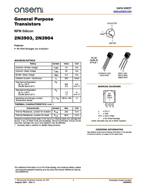
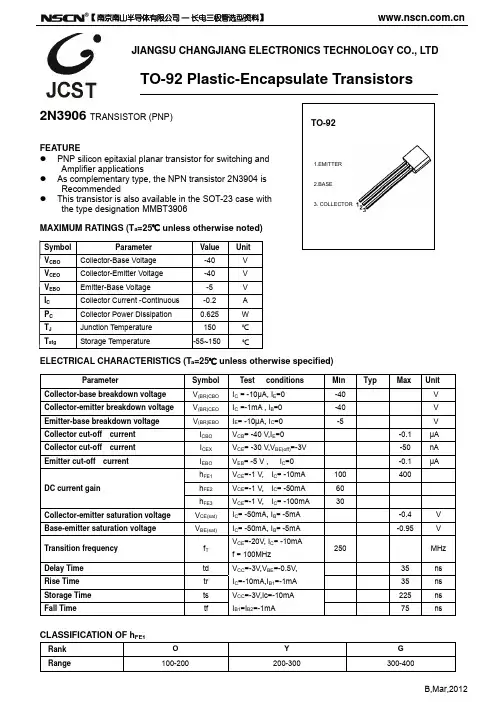
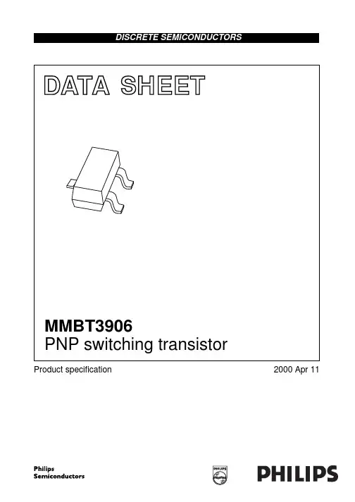
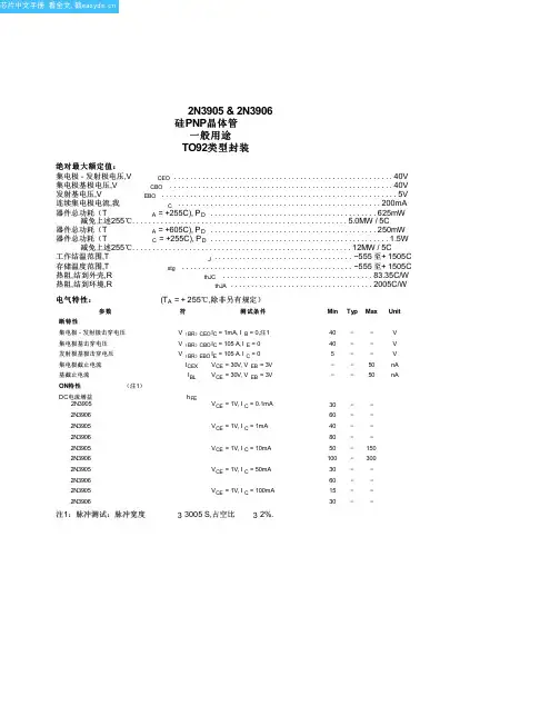
DATA SHEET General PurposeTransistorsNPN Silicon2N3903, 2N3904Features•Pb−Free Packages are Available*MAXIMUM RATINGSRating Symbol Value UnitCollector−Emitter Voltage V CEO40VdcCollector−Base Voltage V CBO60VdcEmitter−Base Voltage V EBO 6.0VdcCollector Current − Continuous I C200mAdcTotal Device Dissipation @ T A = 25°CDerate above 25°C P D6255.0mWmW/°CTotal Device Dissipation@ T C = 25°C Derate above 25°C P D1.512WmW/°COperating and Storage Junction Temperature Range T J, T stg−55 to +150°CTHERMAL CHARACTERISTICS (Note 1)Characteristic Symbol Max Unit Thermal Resistance, Junction−to−Ambient R q JA200°C/W Thermal Resistance, Junction−to−Case R q JC83.3°C/W Stresses exceeding those listed in the Maximum Ratings table may damage the device. If any of these limits are exceeded, device functionality should not be assumed, damage may occur and reliability may be affected.1.Indicates Data in addition to JEDEC Requirements.*For additional information on our Pb−Free strategy and soldering details, please download the onsemi Soldering and Mounting T echniques Reference Manual, SOLDERRM/D.MARKING DIAGRAMSSee detailed ordering and shipping information in the package dimensions section on page 3 of this data sheet.ORDERING INFORMATIONCOLLECTOR21EMITTER2N390xYWW GGx= 3 or 4Y= YearWW= Work WeekG= Pb−Free Package(Note: Microdot may be in either location)BENT LEADTAPE & REELAMMO PACKSTRAIGHT LEADBULK PACKTO−92CASE 29STYLE 1ELECTRICAL CHARACTERISTICS (T A = 25°C unless otherwise noted)Characteristic Symbol Min Max Unit OFF CHARACTERISTICSCollector−Emitter Breakdown Voltage (Note 2)(I C = 1.0 mAdc, I B = 0)V(BR)CEO40−Vdc Collector−Base Breakdown Voltage (I C = 10 m Adc, I E = 0)V(BR)CBO60−Vdc Emitter−Base Breakdown Voltage (I E = 10 m Adc, I C = 0)V(BR)EBO 6.0−Vdc Base Cutoff Current (V CE = 30 Vdc, V EB = 3.0 Vdc)I BL−50nAdc Collector Cutoff Current (V CE = 30 Vdc, V EB = 3.0 Vdc)I CEX−50nAdc ON CHARACTERISTICSDC Current Gain (Note 2)(I C = 0.1 mAdc, V CE = 1.0 Vdc)2N39032N3904 (I C = 1.0 mAdc, V CE = 1.0 Vdc)2N39032N3904 (I C = 10 mAdc, V CE = 1.0 Vdc)2N39032N3904 (I C = 50 mAdc, V CE = 1.0 Vdc)2N39032N3904 (I C = 100 mAdc, V CE = 1.0 Vdc)2N39032N3904h FE204035705010030601530−−−−150300−−−−−Collector−Emitter Saturation Voltage (Note 2) (I C = 10 mAdc, I B = 1.0 mAdc)(I C = 50 mAdc, I B = 5.0 mAdc V CE(sat)−−0.20.3VdcBase−Emitter Saturation Voltage (Note 2) (I C = 10 mAdc, I B = 1.0 mAdc)(I C = 50 mAdc, I B = 5.0 mAdc)V BE(sat)0.65−0.850.95VdcSMALL−SIGNAL CHARACTERISTICSCurrent−Gain − Bandwidth Product(I C = 10 mAdc, V CE = 20 Vdc, f = 100 MHz)2N39032N3904f T250300−−MHzOutput Capacitance (V CB = 5.0 Vdc, I E = 0, f = 1.0 MHz)C obo− 4.0pF Input Capacitance (V EB = 0.5 Vdc, I C = 0, f = 1.0 MHz)C ibo−8.0pFInput Impedance(I C = 1.0 mAdc, V CE = 10 Vdc, f = 1.0 kHz)2N39032N3904h ie1.01.08.010k WVoltage Feedback Ratio(I C = 1.0 mAdc, V CE = 10 Vdc, f = 1.0 kHz)2N39032N3904h re0.10.55.08.0X 10−4Small−Signal Current Gain(I C = 1.0 mAdc, V CE = 10 Vdc, f = 1.0 kHz)2N39032N3904h fe50100200400−Output Admittance (I C = 1.0 mAdc, V CE = 10 Vdc, f = 1.0 kHz)h oe 1.040m mhosNoise Figure(I C = 100 m Adc, V CE = 5.0 Vdc, R S = 1.0 k W, f = 1.0 kHz)2N39032N3904NF−−6.05.0dBSWITCHING CHARACTERISTICSDelay Time(VCC = 3.0 Vdc, V BE = 0.5 Vdc,I C = 10 mAdc, I B1 = 1.0 mAdc)t d−35nsRise Time t r−35nsStorage Time(V CC = 3.0 Vdc, I C = 10 mAdc,2N3903I B1 = I B2 = 1.0 mAdc)2N3904t s−−175200nsFall Time t f−50ns 2.Pulse Test: Pulse Width v 300 m s; Duty Cycle v 2%.ORDERING INFORMATIONDevicePackage Shipping †2N3903RLRM TO −922000 / Ammo Pack 2N3904TO −925000 Units / Bulk 2N3904G TO −92(Pb −Free)5000 Units / Bulk 2N3904RLRA TO −922000 / Tape & Reel 2N3904RLRAG TO −92(Pb −Free)2000 / Tape & Reel 2N3904RLRM TO −922000 / Ammo Pack 2N3904RLRMG TO −92(Pb −Free)2000 / Ammo Pack 2N3904RLRPTO −922000 / Ammo Pack 2N3904RLRPG TO −92(Pb −Free)2000 / Ammo Pack 2N3904RL1G TO −92(Pb−Free)2000 / Tape & Reel 2N3904ZL1TO −922000 / Ammo Pack 2N3904ZL1GTO −92(Pb −Free)2000 / Ammo Pack†For information on tape and reel specifications, including part orientation and tape sizes, please refer to our Tape and Reel Packaging Specifications Brochure, BRD8011/D.Figure 1. Delay and Rise Time Equivalent Test CircuitFigure 2. Storage and Fall Time Equivalent Test Circuit10 < t 1 < 500 m * T otal shunt capacitance of test jig and connectors* T otal shunt capacitance of test jig and connectorsTYPICAL TRANSIENT CHARACTERISTICSFigure 3. CapacitanceREVERSE BIAS VOLTAGE (VOLTS)2.03.05.07.0101.00.1Figure 4. Charge DataI C , COLLECTOR CURRENT (mA)50001.0Q , C H A R G E (p C )3000200010005003002007001005070 2.0 3.0 5.07.01020305070100200C A P A C I T A N C E (p F )1.02.03.0 5.07.010200.20.30.50.7T J = 25°C T J = 125°CFigure 5. Turn −On TimeI C , COLLECTOR CURRENT (mA)7010020030050050Figure 6. Rise TimeI C , COLLECTOR CURRENT (mA)T I M E (n s )5t , R I S E T I M E (n s )Figure 7. Storage Time I C , COLLECTOR CURRENT (mA)Figure 8. Fall TimeI C , COLLECTOR CURRENT (mA)1030720701002003005005051030720701002003005005051030720701002003005005051030720r t , F A L L T I M E (n s )f t , S T O R A G E T I M E (n s )s ′TYPICAL AUDIO SMALL −SIGNAL CHARACTERISTICSNOISE FIGURE VARIATIONS(V CE = 5.0 Vdc, T A = 25°C, Bandwidth = 1.0 Hz)Figure 9. f, FREQUENCY (kHz)46810122Figure 10.R S , SOURCE RESISTANCE (k OHMS)0N F , N O I S E F I G U R E (d B )04681012214N F , N O I S E F I G U R E (d B )Figure 11. Current GainI C , COLLECTOR CURRENT (mA)7010020030050Figure 12. Output AdmittanceI C , COLLECTOR CURRENT (mA)h , C U R R E N T G A I Nh , O U T P U T A D M I T T A N C E ( m h o s )Figure 13. Input Impedance I C , COLLECTOR CURRENT (mA)Figure 14. Voltage Feedback RatioI C , COLLECTOR CURRENT (mA)3010050510202.03.05.07.0101.00.10.21.02.0 5.00.5100.30.5 3.00.72.05.010201.00.20.5o e h , V O L T A G E F E E D B A C K R A T I O (X 10 )r e h , I N P U T I M P E D A N C E (k O H M S )ie 0.10.21.02.0 5.0100.30.5 3.00.10.21.02.0 5.0100.30.5 3.0210.10.21.02.0 5.0100.30.5 3.0f e m -4h PARAMETERS(V CE = 10 Vdc, f = 1.0 kHz, T A = 25°C)TYPICAL STATIC CHARACTERISTICSFigure 15. DC Current GainI C , COLLECTOR CURRENT (mA)0.30.50.71.02.00.2h , D C C U R R E N T G A I N (N O R M A L I Z E D )0.1F EFigure 16. Collector Saturation RegionI B , BASE CURRENT (mA)0.40.60.81.00.2V , C O L L E C T O R E M I T T E R V O L T A G E (V O L T S )0CE Figure 17. “ON” Voltages I C , COLLECTOR CURRENT (mA)0.40.60.81.01.20.2Figure 18. Temperature CoefficientsI C , COLLECTOR CURRENT (mA)V , V O L T A G E (V O L T S )- 0.500.51.0C O E F F I C I E N T (m V / C )- 1.0- 1.5- 2.0°TO−92 (TO−226)CASE 29−11ISSUE AMDATE 09 MAR 2007STYLES ON PAGE 2NOTES:1.DIMENSIONING AND TOLERANCING PER ANSIY14.5M, 1982.2.CONTROLLING DIMENSION: INCH.3.CONTOUR OF PACKAGE BEYOND DIMENSION RIS UNCONTROLLED.4.LEAD DIMENSION IS UNCONTROLLED IN P ANDBEYOND DIMENSION K MINIMUM.SECTION X−XPLANE DIM MIN MAX MIN MAXMILLIMETERSINCHESA0.1750.205 4.45 5.20B0.1700.210 4.32 5.33C0.1250.165 3.18 4.19D0.0160.0210.4070.533G0.0450.055 1.15 1.39H0.0950.105 2.42 2.66J0.0150.0200.390.50K0.500---12.70---L0.250--- 6.35---N0.0800.105 2.04 2.66P---0.100--- 2.54R0.115--- 2.93---V0.135--- 3.43---BENT LEADTAPE & REELAMMO PACKSTRAIGHT LEADBULK PACKNOTES:1.DIMENSIONING AND TOLERANCING PERASME Y14.5M, 1994.2.CONTROLLING DIMENSION: MILLIMETERS.3.CONTOUR OF PACKAGE BEYONDDIMENSION R IS UNCONTROLLED.4.LEAD DIMENSION IS UNCONTROLLED IN PAND BEYOND DIMENSION K MINIMUM.SECTION X−XDIM MIN MAXMILLIMETERSA 4.45 5.20B 4.32 5.33C 3.18 4.19D0.400.54G 2.40 2.80J0.390.50K12.70---N 2.04 2.66P 1.50 4.00R 2.93---V 3.43---STRAIGHT LEADBULK PACKBENT LEADTAPE & REELAMMO PACKMECHANICAL CASE OUTLINEPACKAGE DIMENSIONSTO−92 (TO−226)CASE 29−11ISSUE AMDATE 09 MAR 2007STYLE 1:PIN 1.EMITTER2.BASE3.COLLECTORSTYLE 6:PIN 1.GATE2.SOURCE & SUBSTRATE3.DRAINSTYLE 11:PIN 1.ANODE2.CATHODE & ANODE3.CATHODESTYLE 16:PIN 1.ANODE2.GATE3.CATHODESTYLE 21:PIN 1.COLLECTOR2.EMITTER3.BASESTYLE 26:PIN 1.V CC2.GROUND 23.OUTPUTSTYLE 31:PIN 1.GATE2.DRAIN3.SOURCE STYLE 2:PIN 1.BASE2.EMITTER3.COLLECTORSTYLE 7:PIN 1.SOURCE2.DRAIN3.GATESTYLE 12:PIN 1.MAIN TERMINAL 12.GATE3.MAIN TERMINAL 2STYLE 17:PIN 1.COLLECTOR2.BASE3.EMITTERSTYLE 22:PIN 1.SOURCE2.GATE3.DRAINSTYLE 27:PIN 1.MT2.SUBSTRATE3.MTSTYLE 32:PIN 1.BASE2.COLLECTOR3.EMITTERSTYLE 3:PIN 1.ANODE2.ANODE3.CATHODESTYLE 8:PIN 1.DRAIN2.GATE3.SOURCE & SUBSTRATESTYLE 13:PIN 1.ANODE 12.GATE3.CATHODE 2STYLE 18:PIN 1.ANODE2.CATHODE3.NOT CONNECTEDSTYLE 23:PIN 1.GATE2.SOURCE3.DRAINSTYLE 28:PIN 1.CATHODE2.ANODE3.GATESTYLE 33:PIN 1.RETURN2.INPUT3.OUTPUTSTYLE 4:PIN 1.CATHODE2.CATHODE3.ANODESTYLE 9:PIN 1.BASE 12.EMITTER3.BASE 2STYLE 14:PIN 1.EMITTER2.COLLECTOR3.BASESTYLE 19:PIN 1.GATE2.ANODE3.CATHODESTYLE 24:PIN 1.EMITTER2.COLLECTOR/ANODE3.CATHODESTYLE 29:PIN 1.NOT CONNECTED2.ANODE3.CATHODESTYLE 34:PIN 1.INPUT2.GROUND3.LOGICSTYLE 5:PIN 1.DRAIN2.SOURCE3.GATESTYLE 10:PIN 1.CATHODE2.GATE3.ANODESTYLE 15:PIN 1.ANODE 12.CATHODE3.ANODE 2STYLE 20:PIN 1.NOT CONNECTED2.CATHODE3.ANODESTYLE 25:PIN 1.MT 12.GATE3.MT 2STYLE 30:PIN 1.DRAIN2.GATE3.SOURCESTYLE 35:PIN 1.GATE2.COLLECTOR3.EMITTERON Semiconductor and are registered trademarks of Semiconductor Components Industries, LLC (SCILLC). SCILLC reserves the right to make changes without further notice to any products herein. SCILLC makes no warranty, representation or guarantee regarding the suitability of its products for any particular purpose, nor does SCILLC assume any liability arising out of the application or use of any product or circuit, and specifically disclaims any and all liability, including without limitation special, consequential or incidental damages.“Typical” parameters which may be provided in SCILLC data sheets and/or specifications can and do vary in different applications and actual performance may vary over time. All operating parameters, including “Typicals” must be validated for each customer application by customer’s technical experts. SCILLC does not convey any license under its patent rights nor the rights of others. SCILLC products are not designed, intended, or authorized for use as components in systems intended for surgical implant into the body, or other applications intended to support or sustain life, or for any other application in which the failure of the SCILLC product could create a situation where personal injury or death may occur. Should Buyer purchase or use SCILLC products for any such unintended or unauthorized application, Buyer shall indemnify and hold SCILLC and its officers, employees, subsidiaries, affiliates, and distributors harmless against all claims, costs, damages, and expenses, and reasonable attorney fees arising out of, directly or indirectly, any claim of personal injury or deathassociated with such unintended or unauthorized use, even if such claim alleges that SCILLC was negligent regarding the design or manufacture of the part. SCILLC is an EqualPUBLICATION ORDERING INFORMATIONTECHNICAL SUPPORTNorth American Technical Support:LITERATURE FULFILLMENT :Email Requests to:*******************Europe, Middle East and Africa Technical Support:。