在Altera PFGA上实现POWERLINK从站设计
- 格式:pdf
- 大小:755.77 KB
- 文档页数:15

在Altera的FPGA中实现高速Link口的时序约束方法刘垚;王维;巩玉振;蔡惠智
【期刊名称】《测控技术》
【年(卷),期】2012(031)001
【摘要】在FPGA内部布线资源有限的情况下,将多路TS201 Link口的接口逻辑约束在FPGA固定的区域内并使它达到较高的传输速度,是一件很困难的事情.在Altera的FPGA开发中,正确地利用SDC(synopsys design constraints)时序约束方法和TimeQuest时序分析器可以使这件事情变得容易.详细地讲述了在FPGA 中对多路全双工Link口的接口逻辑进行时序约束的方法,并使Link口的传输速度达到300 MB/s.
【总页数】5页(P116-120)
【作者】刘垚;王维;巩玉振;蔡惠智
【作者单位】中国科学院声学研究所,北京100190;中国科学院声学研究所,北京100190;中国科学院声学研究所,北京100190;中国科学院声学研究所,北京100190
【正文语种】中文
【中图分类】TP271+.82
【相关文献】
1.FPGA中设计FSM实现TigerSHARC DSP link口加载 [J], 夏际金;方志红
2.利用FPGA实现与TS201的LinkPort高速数据互联 [J], 陈春辉;黄俊;陈亚骏
3.利用FPGA实现与TS201的LinkPort高速数据互联 [J], 陈春辉;黄俊;陈亚骏
4.高速Link口通信协议的研究及其FPGA实现 [J], 柴小玲;李红军;姜娇蕊
5.基于FPGA和BWDSP100 Link口的源同步时序约束 [J], 朱鹏;夏际金
因版权原因,仅展示原文概要,查看原文内容请购买。

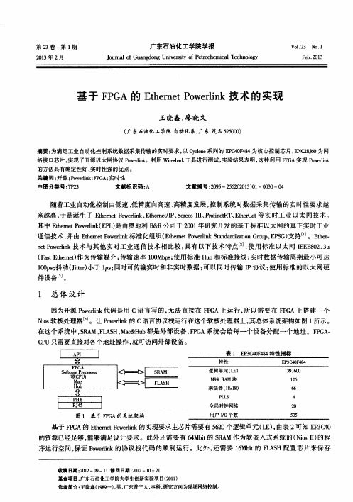
目录1 设计准则 (1)2 模块功能摘要 (1)3 参考资料 (1)4 基本原理 (1)4.1 硬件连接 (2)4.2 操作过程 (3)4.3 数据转换 (4)4.4 在线升级 (5)4.4.1 硬件要求 (6)4.4.2 软件要求 (6)4.4.3具体过程 (6)5 技术指标 (7)6 电原理图 (7)7 PCB图.................................................................................................... 错误!未定义书签。
8 结构图..................................................................................................... 错误!未定义书签。
9 输入、输出接口及性能参数................................................................. 错误!未定义书签。
10 软件 (7)11 元器件说明..................................................................................... 错误!未定义书签。
12 可编程器件说明............................................................................. 错误!未定义书签。
13 可信性设计说明............................................................................. 错误!未定义书签。
14 电源和接地..................................................................................... 错误!未定义书签。

Altera SoC 类FPGA 器件设计难题解决方案
电子发烧友网核心提示:主要FPGA 供应商已经开始销售集成了硬核处理器内核的低成本FPGA 器件,SoC 类FPGA 器件最终会成为主流。
为能够充分发挥所有重要FPGA 的灵活性,这些器件提供了FPGA 设计人员和软件工程师还不熟悉的新特性。
设计人员需要考虑怎样在FPGA 和处理器之间初始化这些资源并进行分配,管理复杂的连接,以及处理器外设的各种设置。
I/O 限制
您可能会说,I/O 有什幺问题?FPGA 有很多I/O!然而,FPGA 现在采用了功能强大的双核Cortex-A9 处理器,需要高性能存储器系统。
如果您不需要处理器,您不用购买器件,因此,连接DDR2/3 存储器来提高性能是最重要的。
这需要72 个专用引脚。
这里不仅有功能强大的处理器,而且还有多种有用的标准外设(例如USB、以太网等)-这就需要更多的引脚。
增加一系列电源和地引脚以实现良好的信号完整性,这会使得以前足够用的BGA 引脚开始显得捉襟见肘。
对于硬件外设,好在这些器件具有复用功能,因此,您可以简单地选择并引出您需要的外设。

基于FPGA的实时以太网(PowerLink)星载通信技术钟铁君;李华旺;常亮【摘要】在卫星中使用以太网的目的是为了在获得灵活的通信接入的同时得到高速的通信速率,并且能满足安全关键场合通信对实时性和确定性的要求.针对国内在空间应用上还未大规模使用以太网这一现实,着眼于解决以太网应用到航天器内部所碰到的实时性、确定性的瓶颈问题,本文对一种有潜力应用到卫星内部的实时以太网(Powerlink)进行研究.在FPGA内部实现Mircoblaze嵌入式系统,外接以太网PHY芯片实现协议栈物理层功能,二者结合为Powerlink协议栈提供运行环境.通过实验验证了设计的可靠性和正确性,可为Poweflink在航天领域的研究与应用提供借鉴.%The main purpose to use Ethernet in satellite is to take advantage of its flexibility to meet the requirement of communicationaccess,simultaneously take into account that Ethernet has high data rates,and expect that it has both real-time and deterministic in safety field.Focus on the situation in China that the Ethernet has not been large-scale used in space,tend to solve the problem of real-time or deterministic encountered inside the spacecraft.A real-time Ethernet (Powerlink)that has the potential to be used in the satellite is studied in this paper.Mircoblaze embedded system is implemented in FPGA and Ethernet chip is externally plugged to realize the physical layer functions of protocol stack,the combination provided the processing environment for Powerlink protocol stack.The reliability and accuracy of the design is proved through experiments and the results of the paper can provide a guideline for Powerlink research in the field of space application.【期刊名称】《电子设计工程》【年(卷),期】2018(026)001【总页数】5页(P144-147,152)【关键词】FPGA;实时以太网;POWERLINK;片上可编程系统【作者】钟铁君;李华旺;常亮【作者单位】中国科学院上海微系统与信息技术研究所上海200050;上海微小卫星工程中心上海201203;中国科学院大学北京101407;中国科学院上海微系统与信息技术研究所上海200050;上海微小卫星工程中心上海201203;中国科学院上海微系统与信息技术研究所上海200050;上海微小卫星工程中心上海201203【正文语种】中文【中图分类】TN913目前国内在航天器上采用的总线主要是CAN总线和1533B总线等传统总线,随着中国航天和空间技术的快速发展,航天器对其内部总线的通信性能提出了越来越高的要求,传统总线的工作方式的已经难以满足航天器对其内部通信系统提出的新要求[1]。

Altera 支持IBM 电源系统服务器,让客户可以采用
FPGA 实现高性能计算解决方案
Altera 公司宣布,最新版Altera 面向OpenCL 的SDK 支持IBM 电源系统服务器作为OpenCL 系统主机。
客户现在可以采用Altera FPGA 实现高性能计算解决方案,针对IBM 电源系统CPU 和加速器电路板来开发OpenCL 代码。
在许多应用上与基于CPU 的标准服务器相比,FPGA 用户可以看到性能提高了5-20 倍。
此外,Altera 公司宣布完全支持OpenPOWER 联盟,这一开放开发联盟使IBM Power 微处理器可以根据许可证下给其他公司进行开放协作和开发。
Altera 公司打算尽快正式加入该联盟,现在等候完成管理文件和开启会籍。
增加IBM 电源系统进一步加强了Altera 基于FPGA 的异构计算产品,而且还支持所有其他主要体系结构。
Altera 军事、工业和计算业务部资深副总裁兼总经理Jeff Waters 评论说:“高性能IBM 电源系统与FPGA 应用加速功能相结合,Altera 面向OpenCL
的SDK 为客户提供了无与伦比的异构计算环境。
世界上最前沿的高性能计算系统和数据中心服务器开发人员使用了Altera 面向OpenCL 的SDK,借助今天的新闻发布,我们为这些客户提供了更多的计算体系结构选择。
”。
Altera中文资料FPGA在软件无线电中的应用介绍软件无线电(SDR)是具有可重配置硬件平台的无线设备,可以跨多种通信标准。
它们因为更低的成本、更大的灵活性和更高的性能,迅速称为军事、公共安全和商用无线领域的事实标准。
SDR成为商用流行的主要原因之一是它能够对多种波形进行基带处理和数字中频(IF)处理。
IF处理将数字信号处理的领域从基带扩展到RF。
支持基带和中频处理的能力增加了系统灵活性,同时减小了制造成本。
基带处理无线标准不断地发展,通过先进的基带处理技术如自适应调制编码、空时编码(STC)、波束赋形和多入多出(MIMO)天线技术,支持更高的数据速率。
基带信号处理器件需要巨大的处理带宽,以支持这些技术中大计算量的算法。
例如,美国军事联合战术无线系统(JTRS)定义了军事无线中20多种不同的无线波形。
一些更复杂的波形所需的计算能力在标准处理器上是每秒数百万条指令(MIPS),或者如果在FPGA 实现是数千个逻辑单元。
协处理器特性SDR基带处理通常需要处理器和FPGA。
在这类应用中,处理器处理系统控制和配置功能,而FPGA实现大计算量的信号处理数据通道和控制,让系统延迟最小。
当需要从一种标准切换至另一种标准时,处理器能够动态地在软件的主要部分间切换,而FPGA能够根据需要完全重新配置,实现特定标准的数据通道。
FPGA可以作为协处理器同DSP和通用处理相连,这样具有更高的系统性能和更低的系统成本。
自由地选择在哪实现基带处理算法为实现SDR算法提供了另一种方式的灵活性。
基带部件也需要足够灵活让所需的SDR功能支持在同一种标准增强版本之间的移植,并能够支持完全不同的标准。
可编程逻辑结合软核处理器和IP,具有了提供在现场远程升级的能力。
图1 是一个框图,其中FPGA能够通过IP功能如Turbo编码器、Reed-Solomon编码器、符号交织器、符号映射器和IFFT,很容易地重配置支持WCDMA/HSPDA或802.16a标准的基带发送功能。
基于Altera和Xilinx FPGA的POWERLINK从站方案佚名
【期刊名称】《自动化仪表》
【年(卷),期】2011(32)5
【摘要】通过基于FPGA的POWERLINK从站,贝加莱现在可以为自动化组件制造商提供理想的解决方案,即将实时以太网连接广泛地添加到贝加莱的产品中。
这种统一的解决方案可以在所有低成本的产品中实现,如带有极少电子零件的紧凑型传感器、功能强大的驱动器和模块化I/O总线连接模块等。
【总页数】1页(P5-5)
【关键词】FPGA;Xilinx;Altera;从站;连接模块;自动化组件;实时以太网;I/O总线【正文语种】中文
【中图分类】TP311.11
【相关文献】
1.单微处理器实现单网口Open Powerlink从站通信解决方案 [J], 文长明;项曦文;柴桂锋;储成君;尹若嵬
2.单微处理器实现双网口Open Powerlink从站通信解决方案 [J], 文长明;项曦文;柴桂锋;储成君;尹若嵬
3.Altera利用低成本低功耗CPLD,扩展便携式市场/XILINX发布ISE WEBPACK 8.2i FPGA行业唯一免费的全功能设计套件 [J],
4.泰克与躐合作为XILINX FPGA提供实时逻辑调试方案泰克TLA系列逻辑分析仪和FS2 FPGA View软件为XILINX FPGA提供完整的调试套件 [J],
5.Xilinx FPGA处理器解决方案为嵌入式系统设计人员提供强大的性能优势独立测
试结果再次肯定了Xilinx业界最全面的基于FPGA的32位嵌入式处理解决方案的领先地位 [J],
因版权原因,仅展示原文概要,查看原文内容请购买。
User Guide openPowerlink FPGA Slave Reference Design Author: Zelenka Joerg Version: V1.0Date: 27/10/2009File: User Guide.docINDEX1Document Overview (3)2Design Features (3)3Performance Restriction (3)4Requirements (3)5Quick Start (4)5.1Unzip Package (4)5.2Build Makefile (5)5.3Program FPGA (Hardware) (6)5.4Program Nios II CPU (Software) (7)5.5Run a Nios II Terminal (immediate debugging) (8)6Quartus II (8)7Nios II IDE (9)7.1Import Software Projects (9)7.2Configure Target Connection (12)7.3Run or Debug Target (12)8Troubleshooting (13)1 Document OverviewThis document gives you a “Quick Start” instruction (5 @ page 4) to successfully run the openPowerlink FPGA Slave Reference Design in a few minutes. In addition the performance restrictions (3 @ page 3) are given and should be considered at any time!In chapter 6 the steps are given to import the software projects into Nios II IDE to start development. In case of error messages please refer to section 8 starting at page 13.2 Design FeaturesThe openPowerlink FPGA Slave Reference Design uses one TXPDO and two RXPDOs (refer to Table 2-1).Table 2-1: PDOsSource/Sink on EvalBoard I/O Size PDO IndexInput 8 Bits (lower nibble used) 0x60004 Buttons(below 7-Segment Display)6 LEDsOutput 8 Bits (upper six bits used 2) 0x6200 (above Buttons)Output 16 Bits 0x630016 Outputs(24V I/O Header) 1Table Note:1.The 24V I/O stage needs an extra 24V supply!Please refer to the DBC3C40’s Datasheet (Version 1.10) at page 33!2.LED0 and LED1 are used as CN Status- and Error-LEDs.3 Performance RestrictionIt is recommended considering the following restrictions (Table 3-1) to run a stable Powerlink Network with the provided openPowerlink FPGA Slave!Table 3-1: performance restrictionsPowerlink Cycle Time 4 400 µs (min) Input Process Data per Cycle 1 3 (max)Input Process Data volume per Cycle 1, 2 36 Bytes (max) Output Process Data volume per Cycle 2 36 Bytes (max) Asynchronous Data MTU (ASnd …) 3, 5 1514Bytes (max) Table Note:1.Per Powerlink Cycle it is allowed to receive the maximum data volume (EPLPayload) within one PDO (PReq) or three PDOs (PReq, PRes MN and PRes CrossTraffic).2.EPL Payload3.asynchronous phase (between SoA and SoC)piler Optimization Level must be the highest (-O2)5.Ethernet Frame excl. CRCIt is recommended to read the openMAC’s documentation (docu_openMacv12.pdf, focus on chapter “Application Note”) and openPowerlink specific documents (e.g. from SysTec …) before performing any changes to the Reference Design (changes in hardware or software)!4 Requirements•Development Board EBV DBC3C40 (Mercury Board)•Altera Quartus II v9.0 or newer (Web Edition is also possible)•Altera Nios II Embedded Design Suite v9.0 or newer•Optional with “DBC3C40_Setup.exe for Quartus 9.0” installation to program the reference design non-volatile into the device (refer to the newest DBC3C40 datasheet – version 1.10 or newer)•Experiences with this development environment are required•POWERLINK network as described in main readme.txt•openPowerlink Stack V1.5.9.6Usually the FPGA Slave Reference Design will be delivered separately in a Zip-file (“openPOWERLINK_openMAC_v1.5.9.6.zip” … Reference Design with openMAC + Nios II).The openPowerlink Stack is located in the file “openPOWERLINK_v1.5.9.6.zip”.5 Quick StartThis chapter helps you to run the openPowerlink FPGA Slave Reference Design. It is crucial to follow these instructions by order:1.Unzip Package2.Build Makefile3.Program FPGA (Hardware)4.Program Nios II CPU (Software)5.Run a Nios II Terminal (immediate debugging)In case of errors refer to section 8!The package will be copied into a directory which can differ. So, in this guide it will be called “MYROOT”.5.1 Unzip PackagePlease follow these instructions in the right order!1.Unzip the openPowerlink Stack Source Files out of the fileopenPOWERLINK_v1.5.9.6.zip into your directory MYROOT.2.Unzip the FPGA Slave specific Source Files (openMAC and System HardwareDesign, Drivers …) out of the file openPOWERLINK_openMAC_v1.5.9.6.zip into the same directory (MYROOT) as before.pare MYROOT with the in Figure 5-1 given structure.Figure 5-1: reference design directory5.2 Build MakefileIf you have successfully unzipped the reference design project, you can build the Makefile for the software compilation. Please follow the following steps!1.Open Nios II Command Shell out of the Start Menu (Start – Programs – Altera –Nios II EDS 9.0 - Nios II 9.0 Command Shell).You can find an example command shell in Figure 5-2.2.Change to your drive (usually C) by typing incd c:3.Change to the directoryMYROOT/openPOWERLINK_v1.5.9.6/Examples/altera_nios2/no_os/gnu/demo_cn _3r1tpdo by typing in (no line break!)cd myroot/openPOWERLINK_v1.5.9.6/Examples/altera_nios2/no_os/gnu/demo_cn_3r1tpdo4.Run the script “create-this-app” with typing into the shell. The script execution willlast some minutes (depends on your PC)../create-this-app5.Don’t exit the command shell, because you will need it for downloading theapplication to the Nios II CPU!Figure 5-2: example command shell5.3 Program FPGA (Hardware)The next step is to program the hardware design into the FPGA. This is done with the Programmer Tool in Quartus II. Follow the next steps carefully!1.Open Quartus II (usually on Desktop or via Start Menu: Start – Programs – Altera– Quartus II 9.0 – Quartus II 9.0)2.Open the openPowerlink FPGA Slave Reference Hardware ProjectFile – Open Project …3.Browse to the Reference Design atMYROOT\openPOWERLINK_v1.5.9.6\Examples\altera_nios2\EBV_DBC3C40\design_nios2_openmac4.Select “nios_openMac.qpf” and open the Quartus II Project File5.Click in Quartus II Tools – Programmer6.Verify if your EBV Board is connected to a power source and to your PC (e.g. viaUSB Blaster)!7.You can directly start the programming, because you have already opened theQuartus II Project File! So, click Start.8.The binary download is done within some seconds and is indicated with theprogress bar at top right.9.You can exit the Programmer and Quartus II if you like.Figure 5-3: Quartus II Programmer example (progress done)5.4 Program Nios II CPU (Software)After downloaded the Hardware Design into the FPGA (done in section 5.3) you have the ability to access the Nios II CPU via JTAG. The software application can be downloaded ina command shell.1.Open a Nios II Command Shell or use the one you have already opened in section5.2.2.Type the following command into the shellmake download-elf3.Verify if the elf-download was done without any error (refer to Figure 5-4).Figure 5-4: command shell download application5.5 Run a Nios II Terminal (immediate debugging)After downloading the Hardware Design into the FPGA (section 5.3) and programmed the Nios II CPU (section 5.4), the openPowerlink FPGA Slave is ready to operate. You can obtain further information via the JTAG interface. Follow these steps:1.Open a new Nios II Command Shell out of the Start Menu (Start – Programs –Altera – Nios II EDS 9.0 - Nios II 9.0 Command Shell).2.Type into the shell the following commandnios2-terminal3.Now you can see STDOUT messages (refer to Figure 5-5).Figure 5-5: Nios II Terminal example6 Quartus IIQuartus II includes a hardware development environment to build hardware designs for Altera FPGAs. The reference design’s top level was built in a schematic file (refer to Figure 6-1).You can use directly the reference design for building your specific openPowerlink Slave (CN) application. Please refer to the openMAC’s documentation (docu_openMacv12.pdf, focus on chapter “Application Note”)!Figure 6-1: Quartus II with opened reference design 7 Nios II IDEAltera provides a software development environment called Nios II IDE. TheopenPowerlink FPGA Slave Reference Design application can be imported into the IDE. Before doing that you need to build a Makefile considering the following arguments by calling the “create-this-app” script in the Nios II Command Shell. ./create-this-app ...Instead of the “...” you can add arguments. The meaning is given in Table 7-1. These arguments can be used in combination. No argument is allowed if you build the Makefile the first time (no current Makefile is available).Table 7-1: arguments' meaning --rebuild This argument causes the deletion of the current Makefile and rebuilds a new one. Should be used after changing the Hardware System in theSOPC.--debug This argument builds a Makefile with the highest compiler optimizationlevel. Should be used when debugging the Nios II CPU’s softwareapplication.Example: rebuild Makefile and change optimization level to none (for debugging) ./create-this-app --rebuild --debug7.1 Import Software ProjectsFollow these steps to successfully import the openPowerlink Reference Software Project:1. Run Nios II IDE (usually on desktop or via Start Menu Start – Programs – Altera –Nios II EDS 9.0 - Nios II 9.0 IDE2. Follow the instructions if you run IDE the first time!3. Click File – Import4.Expand Altera Nios II and select “Existing Nios II software build tools project orfolder into workspace” (refer to Figure 7-1)5.Next6.Browse to MYROOT\openPOWERLINK_v1.5.9.6 (ignore warnings!) to get theopenPowerlink Stack Source Files (refer to Figure 7-2)7.Finish8.Click File – Import again9.Expand Altera Nios II and select “Existing Nios II software build tools project orfolder into workspace” (refer to Figure 7-1)10.Next11.Browse to MYROOT\openPOWERLINK_v1.5.9.6\Examples\altera_nios2\no_os\gnu\demo_cn_3r1tpdo (ignore warnings!) to get the example application of a CN (refer to Figure 7-3)12.FinishFigure 7-1: import existing software projectFigure 7-2: import openPowerlink Stack sourcesFigure 7-3: import the example application7.2 Configure Target ConnectionFor starting debugging or running sessions you need to configure a Nios II Hardware configuration. Follow these steps (refer to Figure 7-4):1.Click Run – Run…2.Select Nios II Hardware and click on the new button3.An error will occur, because the *.ptf file (create by SOPC) was not found.4.Click brows at the Target Hardware Section5.Browse toMYROOT\openPOWERLINK_v1.5.9.6\Examples\altera_nios2\EBV_DBC3C40\design_nios2_openmac6.Select the file niosII_openMac.ptf7.Click Close and Save Changes!Figure 7-4: configure target7.3 Run or Debug TargetYou can run or debug the target via the buttons in Nios II IDE or via the menu Run – Run… or Run – Debug…Always verify if the EBV Board is connected to a power source and to your computer via the USB Blaster box.Figure 7-5: Nios II IDE with application example 8 TroubleshootingThis chapter comprises a collection of possible errors that may occur when running through this user guide.“!”....................Trouble“ ”...................Solution! When running Nios II IDE in debug mode an error message appears.An other Nios II Terminals (e.g. in a Command Shell or IDE) is running and connected to your target. Close the other terminal session!! A Nios II Terminal is running (e.g. in IDE) but it is not possible to stop this session. Open the Task Manager and stop the task “nios2-terminal.exe”.! When stepping through the application source (debug mode in IDE), the instructions won’t be executed line by line.The compiler optimization level is unequal none. You need to create the Makefile again with the argument --debug (refer to Table 7-1).! When compiling the reference design with Quartus II, the following error is reported. The delivered Quartus II Project is incomplete to minimize the package’s size. So, temporary files had been deleted!Open SOPC and generate the Nios II system, to compile the Quartus II Projectsuccessfully.! When trying to program the FPGA with the Quartus II Programmer the following error (for further information refer to Altera Support sources) is shown:A Nios II Terminal is running and blocking the access to the FPGA. Close thisconnection or terminate the “nios2-terminal.exe” task in the Task Manager.! When trying to build the Makefile an error is shown in the command shell.The Makefile was already built, so you can only rebuild the Makefile with the appropriate argument (refer to Table 7-1).! When downloading the application the Nios II CPU the following error appears (for further information refer to Altera Support sources).The Nios II CPU on the FPGA is not the CPU from the reference design. Reprogram your FPGA (refer to 5.3).。