Scalable trigger processing
- 格式:pdf
- 大小:88.54 KB
- 文档页数:10
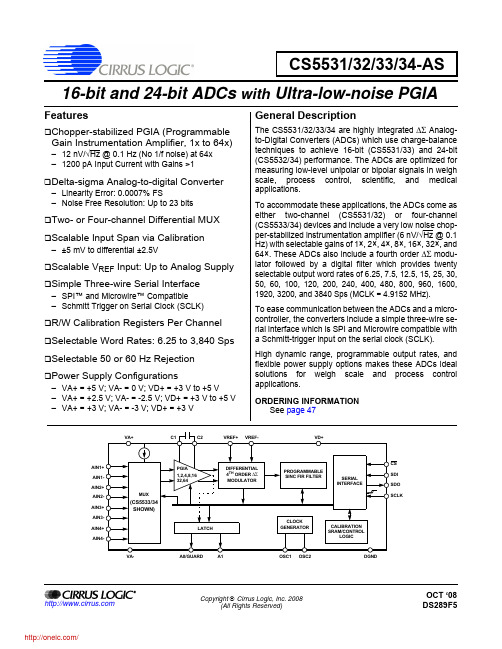
Copyright © Cirrus Logic, Inc. 2008CS5531/32/33/34-AS16-bit and 24-bit ADCs with Ultra-low-noise PGIAFeaturesChopper-stabilized PGIA (ProgrammableGain Instrumentation Amplifier, 1x to 64x)–12 nV/√Hz @ 0.1 Hz (No 1/f noise) at 64x –1200pA Input Current with Gains >1 Delta-sigma Analog-to-digital Converter –Linearity Error: 0.0007% FS–Noise Free Resolution: Up to 23 bits Two- or Four-channel Differential MUX Scalable Input Span via Calibration –±5 mV to differential ±2.5VScalable V REF Input: Up to Analog Supply Simple Three-wire Serial Interface –SPI™ and Microwire™ Compatible –Schmitt Trigger on Serial Clock (SCLK) R/W Calibration Registers Per Channel Selectable Word Rates: 6.25 to 3,840 Sps Selectable 50 or 60 Hz RejectionPower Supply Configurations–VA+ = +5 V; VA- = 0 V; VD+ = +3 V to +5 V–VA+ = +2.5 V; VA- = -2.5 V; VD+ = +3 V to +5 V –VA+ = +3 V; VA- = -3 V; VD+ = +3 VGeneral DescriptionThe CS5531/32/33/34 are highly integrated ∆Σ Analog-to-Digital Converters (ADCs) which use charge-balance techniques to achieve 16-bit (CS5531/33) and 24-bit (CS5532/34) performance. The ADCs are optimized for measuring low-level unipolar or bipolar signals in weigh scale, process control, scientific, and medical applications.To accommodate these applications, the ADCs come as either two-channel (CS5531/32) or four-channel (CS5533/34) devices and include a very low noise chop-per-stabilized instrumentation amplifier (6 nV/√Hz @ 0.1Hz) with selectable gains of 1×, 2×, 4×, 8×, 16×, 32×, and 64×. These ADCs also include a fourth order ∆Σ modu-lator followed by a digital filter which provides twenty selectable output word rates of 6.25, 7.5, 12.5, 15, 25, 30,50, 60, 100, 120, 200, 240, 400, 480, 800, 960, 1600,1920, 3200, and 3840 Sps (MCLK =4.9152MHz).To ease communication between the ADCs and a micro-controller, the converters include a simple three-wire se-rial interface which is SPI and Microwire compatible with a Schmitt-trigger input on the serial clock (SCLK).High dynamic range, programmable output rates, and flexible power supply options makes these ADCs ideal solutions for weigh scale and process control applications.ORDERING INFORMATIONSee page 47VA+C1C2VREF+VREF-VD+DIFFERENTIAL 4TH ORDER ∆ΣMODULATORPGIA 1,2,4,8,16PROGRAMMABLE SINC FIR FILTERMUX(CS5533/34SHOWN)AIN1+AIN1-AIN2+AIN2-AIN3+AIN3-AIN4+AIN4-SERIAL INTERFACELATCHCLOCK GENERATORCALIBRATION SRAM/CONTROLLOGICDGNDCSSDI SDO SCLKOSC2OSC1A1A0/GUARD VA-32,64OCT ‘08TABLE OF CONTENTS1.CHARACTERISTICS AND SPECIFICATIONS (4)ANALOG CHARACTERISTICS (4)TYPICAL RMS NOISE (NV), CS5531/32/33/34 (7)TYPICAL NOISE-FREE RESOLUTION(BITS), CS5532/34 (7)5 V DIGITAL CHARACTERISTICS (8)3 V DIGITAL CHARACTERISTICS (8)DYNAMIC CHARACTERISTICS (9)ABSOLUTE MAXIMUM RATINGS (9)SWITCHING CHARACTERISTICS (10)2.GENERAL DESCRIPTION (12)2.1.Analog Input (12)2.1.1. Analog Input Span (13)2.1.2. Multiplexed Settling Limitations (13)2.1.3. Voltage Noise Density Performance (13)2.1.4. No Offset DAC (14)2.2.Overview of ADC Register Structure and Operating Modes (14)2.2.1. System Initialization (15)2.2.2. Serial Port Interface (22)2.2.3. Reading/Writing On-Chip Registers (23)2.3.Configuration Register (23)2.3.1. Power Consumption (23)2.3.2. System Reset Sequence (23)2.3.3. Input Short (24)2.3.4. Guard Signal (24)2.3.5. Voltage Reference Select (24)2.3.6. Output Latch Pins (24)2.3.7. Offset and Gain Select (25)2.3.8. Filter Rate Select (25)2.4.Setting up the CSRs for a Measurement (27)2.5.Calibration (30)2.5.1. Calibration Registers (30)2.5.2. Performing Calibrations (31)2.5.3. Self-calibration (31)2.5.4. System Calibration (32)2.5.5. Calibration Tips (32)2.5.6. Limitations in Calibration Range (33)2.6.Performing Conversions (33)2.6.1. Single Conversion Mode (33)2.6.2. Continuous Conversion Mode (34)2.6.3. Examples of Using CSRs to Perform Conversions and Calibrations (35)ing Multiple ADCs Synchronously (36)2.8.Conversion Output Coding (36)2.9.Digital Filter (38)2.10.Clock Generator (39)2.11.Power Supply Arrangements (39)2.12.Getting Started (43)2.13.PCB Layout (43)3.PIN DESCRIPTIONS (44)4.SPECIFICATION DEFINITIONS (46)5.ORDERING INFORMATION (47)6.ENVIRONMENTAL, MANUFACTURING, & HANDLING INFORMATION (47)7.PACKAGE DRAWINGS (48)LIST OF FIGURESFigure 1. SDI Write Timing (Not to Scale) (11)Figure 2. SDO Read Timing (Not to Scale) (11)Figure 3. Multiplexer Configuration (12)Figure 4. Input models for AIN+ and AIN- pins (13)Figure 5. Measured Voltage Noise Density (13)Figure 6. CS5531/32/33/34 Register Diagram (14)Figure 7. Command and Data Word Timing (22)Figure 8. Guard Signal Shielding Scheme (24)Figure 9. Input Reference Model when VRS = 1 (25)Figure 10. Input Reference Model when VRS = 0 (25)Figure 11. Self-calibration of Offset (32)Figure 12. Self-calibration of Gain (32)Figure 13. System Calibration of Offset (32)Figure 14. System Calibration of Gain (32)Figure 15. Synchronizing Multiple ADCs (36)Figure 16. Digital Filter Response (Word Rate = 60 Sps) (38)Figure 17. 120 Sps Filter Magnitude Plot to 120 Hz (38)Figure 18. 120 Sps Filter Phase Plot to 120 Hz (38)Figure 19. Z-Transforms of Digital Filters (38)Figure 20. On-chip Oscillator Model (39)Figure 21. CS5532 Configured with a Single +5 V Supply (40)Figure 22. CS5532 Configured with ±2.5 V Analog Supplies (41)Figure 23. CS5532 Configured with ±3 V Analog Supplies (41)Figure 24. CS5532 Configured for Thermocouple Measurement (42)Figure 25. Bridge with Series Resistors (42)LIST OF TABLESTable 1. Conversion Timing – Single Mode (34)Table 2. Conversion Timing – Continuous Mode (34)Table 3. Command Byte Pointer (35)Table 4. Output Coding for 16-bit CS5531 and CS5533 (36)Table 5. Output Coding for 24-bit CS5532 and CS5534 (37)1. CHARACTERISTICS AND SPECIFICATIONSANALOG CHARACTERISTICS(VA+, VD+ = 5 V ±5%; VREF+ = 5 V; VA-, VREF-, DGND = 0 V; MCLK = 4.9152 MHz; OWR (Output Word Rate) = 60 Sps; Bipolar Mode; Gain = 32)(See Notes 1 and 2.)Notes: 1.Applies after system calibration at any temperature within -40 °C ~ +85 °C.2.Specifications guaranteed by design, characterization, and/or test. LSB is 16 bits for the CS5531/33 andLSB is 24 bits for the CS5532/34.3. This specification applies to the device only and does not include any effects by external parasiticthermocouples.4.Drift over specified temperature range after calibration at power-up at 25 °C.ParameterCS5531/CS5533Unit Min Typ Max Accuracy Linearity Error -±0.0015±0.003%FS No Missing Codes 16--Bits Bipolar Offset -±1±2LSB 16Unipolar Offset-±2±4LSB 16Offset Drift(Notes 3 and 4)-10-nV/°C Bipolar Full-scale Error -±8±31ppm Unipolar Full-scale Error -±16±62ppm Full-scale Drift(Note 4)-2-ppm/°CParameterCS5532/CS5534Unit Min Typ Max Accuracy Linearity Error -±0.0015±0.003%FS No Missing Codes 24--Bits Bipolar Offset -±16±32LSB 24Unipolar Offset-±32±64LSB 24Offset Drift(Notes 3 and 4)-10-nV/°C Bipolar Full-scale Error -±8±31ppm Unipolar Full-scale Error -±16±62ppm Full-scale Drift(Note 4)-2-ppm/°CANALOG CHARACTERISTICS (Continued)(See Notes 1 and 2.)Notes: 5.The voltage on the analog inputs is amplified by the PGIA, and becomes V CM ± Gain*(AIN+ - AIN-)/2 atthe differential outputs of the amplifier. In addition to the input common mode + signal requirements for the analog input pins, the differential outputs of the amplifier must remain between (VA- + 0.1 V) and (VA+ - 0.1 V) to avoid saturation of the output stage.6.See the section of the data sheet which discusses input models.7.Input current on AIN+ or AIN- (with Gain =1), or VREF+ or VREF- may increase to 250nA if operatedwithin 50mV of VA+ or VA-. This is due to the rough charge buffer being saturated under these conditions.ParameterMin TypMaxUnitAnalog InputCommon Mode + Signal on AIN+ or AIN-Bipolar/Unipolar ModeGain = 1 Gain = 2, 4, 8, 16, 32, 64(Note 5)VA-VA- + 0.7--VA+VA+ - 1.7V V CVF Current on AIN+ or AIN-Gain = 1 (Note 6, 7)Gain = 2, 4, 8, 16, 32, 64--501200--nA pA Input Current Noise Gain = 1 Gain = 2, 4, 8, 16, 32, 64--2001--pA/√Hz pA/√Hz Input Leakage for Mux when Off (at 25 °C)-10-pA Off-channel Mux Isolation -120-dB Open Circuit Detect Current 100300-nA Common Mode Rejection dc, Gain = 1dc, Gain = 6450, 60 Hz ---90130120---dB dB dB Input Capacitance -60-pF Guard Drive Output -20-µA Voltage Reference Input Range (VREF+) - (VREF-)1 2.5(VA+)-(VA-)V CVF Current (Note 6, 7)-50-nA Common Mode Rejection dc 50, 60 Hz --120120--dB dB Input Capacitance 11-22pF System Calibration Specifications Full-scale Calibration Range Bipolar/Unipolar Mode 3-110%FS Offset Calibration Range Bipolar Mode -100-100%FS Offset Calibration Range Unipolar Mode -90-90%FSANALOG CHARACTERISTICS (Continued)(See Notes 1 and 2.)8.All outputs unloaded. All input CMOS levels.9.Power is specified when the instrumentation amplifier (Gain ≥ 2) is on. Analog supply current is reducedby approximately 1/2 when the instrumentation amplifier is off (Gain = 1).10.Tested with 100 mV change on VA+ or VA-.ParameterMinTypMaxUnitPower SuppliesDC Power Supply Currents (Normal Mode)I A+, I A-I D+- - 60.681mA mA Power ConsumptionNormal Mode (Notes 8 and 9)Standby Sleep---35550045--mW mW µW Power Supply Rejection (Note 10)dc Positive Supplies dc Negative Supply--115115--dB dBTYPICAL RMS NOISE (nV), CS5531/32/33/34(See notes 11, 12 and 13)Notes:11.Wideband noise aliased into the baseband. Referred to the input. Typical values shown for 25 °C.12.For peak-to-peak noise multiply by 6.6 for all ranges and output rates.13.Word rates and -3dB points with FRS = 0. When FRS = 1, word rates and -3dB points scale by 5/6.TYPICAL NOISE-FREE RESOLUTION(BITS), CS5532/34 (See Notes 14 and 15)14.Noise-free resolution listed is for bipolar operation, and is calculated as LOG((Input Span)/(6.6xRMSNoise))/LOG(2) rounded to the nearest bit. For unipolar operation, the input span is 1/2 as large, so one bit is lost. The input span is calculated in the analog input span section of the data sheet. The noise-free resolution table is computed with a value of 1.0 in the gain register. Values other than 1.0 will scale the noise, and change the noise-free resolution accordingly.15.“Noise-free resolution” is not the same as “effective resolution”. Effective resolution is based on theRMS noise value, while noise-free resolution is based on a peak-to-peak noise value specified as 6.6 times the RMS noise value. Effective resolution is calculated as LOG((Input Span)/(RMS Noise))/LOG(2).Specifications are subject to change without notice.Output Word Rate (Sps)-3 dB Filter Frequency (Hz)Instrumentation Amplifier Gainx64x32x16x8x4x2x17.5 1.9417171926427915515 3.882425273659111218307.7534353951841573086015.548495472118222436120316870771021673146162406211516027652710402070415048012216323039274814802950589096023022932155410602090417083401,920390344523946184036507290146003,84078013902710539010800215004300086100Output Word Rate (Sps)-3 dB Filter Frequency (Hz)Instrumentation Amplifier Gain x64x32x16x8x4x2x17.5 1.941920212222222215 3.8819202121212222307.75181920212121216015.5181920202021211203117181920202020240621617171717171748012216171717171717960230151616161616161,920390151515151515153,840780131313131313135 V DIGITAL CHARACTERISTICS(VA+, VD+ = 5 V ±5%; VA-, DGND = 0 V;See Notes 2 and 16.)3 V DIGITAL CHARACTERISTICS(T A = 25 °C; VA+ = 5V ±5%; VD+ = 3.0V±10%; VA-, DGND = 0V; See Notes 2 and 16.)16.All measurements performed under static conditions.ParameterSymbol Min Typ Max Unit High-level Input Voltage All Pins Except SCLKSCLK V IH 0.6 VD+(VD+) - 0.45--VD+VD+V Low-level Input Voltage All Pins Except SCLKSCLK V IL 0.00.0-0.80.6V High-level Output Voltage A0 and A1, I out = -1.0 mASDO, I out = -5.0 mA V OH (VA+) - 1.0(VD+) - 1.0--V Low-level Output Voltage A0 and A1, I out = 1.0 mASDO, I out = 5.0 mAV OL --(VA-) + 0.40.4V Input Leakage Current I in -±1±10µA SDO Tri-state Leakage Current I OZ --±10µA Digital Output Pin CapacitanceC out-9-pFParameterSymbol Min Typ Max Unit High-level Input Voltage All Pins Except SCLKSCLK V IH 0.6 VD+(VD+) - 0.45-VD+VD+V Low-level Input Voltage All Pins Except SCLKSCLK V IL 0.00.0-0.80.6V High-level Output Voltage A0 and A1, I out = -1.0 mASDO, I out = -5.0 mA V OH (VA+) - 1.0(VD+) - 1.0--V Low-level Output Voltage A0 and A1, I out = 1.0 mASDO, I out = 5.0 mAV OL --(VA-) + 0.40.4V Input Leakage Current I in -±1±10µA SDO Tri-state Leakage Current I OZ --±10µA Digital Output Pin CapacitanceC out-9-pFDYNAMIC CHARACTERISTICS17.The ADCs use a Sinc 5 filter for the 3200 Sps and 3840 Sps output word rate (OWR) and a Sinc 5 filterfollowed by a Sinc 3 filter for the other OWRs. OWR sinc5 refers to the 3200 Sps (FRS = 1) or 3840 Sps (FRS = 0) word rate associated with the Sinc 5 filter.18.The single conversion mode only outputs fully settled conversions. See Table 1 for more details aboutsingle conversion mode timing. OWR SC is used here to designate the different conversion time associated with single conversions.19.The continuous conversion mode outputs every conversion. This means that the filter’s settling timewith a full-scale step input in the continuous conversion mode is dictated by the OWR.ABSOLUTE MAXIMUM RATINGS(DGND = 0 V; See Note 20.)Notes:20.All voltages with respect to ground.21.VA+ and VA- must satisfy {(VA+) - (VA-)} ≤ +6.6 V.22.VD+ and VA- must satisfy {(VD+) - (VA-)} ≤ +7.5 V.23.Applies to all pins including continuous overvoltage conditions at the analog input (AIN) pins.24.Transient current of up to 100 mA will not cause SCR latch-up. Maximum input current for a power supply pin is ±50 mA.25.Total power dissipation, including all input currents and output currents.WARNING:Operation at or beyond these limits may result in permanent damage to the device.Normal operation is not guaranteed at these extremes.ParameterSymbol Ratio Unit Modulator Sampling Ratef s MCLK/16Sps Filter Settling Time to 1/2 LSB (Full-scale Step Input)Single Conversion mode (Notes 17, 18, and 19)Continuous Conversion mode, OWR < 3200 Sps Continuous Conversion mode, OWR ≥ 3200 Spst s t s t s1/OWR SC5/OWR sinc5 + 3/OWR5/OWRs s sParameterSymbol Min Typ Max Unit DC Power Supplies(Notes 21 and 22)Positive Digital Positive Analog Negative Analog VD+VA+VA--0.3-0.3+0.3---+6.0+6.0-3.75V V V Input Current, Any Pin Except Supplies (Notes 23 and 24)I IN --±10mA Output Current I OUT--±25mA Power Dissipation (Note 25)PDN --500mW Analog Input Voltage VREF pins AIN PinsV INR V INA (VA-) -0.3(VA-) -0.3--(VA+) + 0.3(VA+) + 0.3V V Digital Input VoltageV IND -0.3-(VD+) + 0.3V Ambient Operating Temperature T A -40-85°C Storage Temperature T stg-65-150°CSWITCHING CHARACTERISTICS(VA+ = 2.5 V or 5 V ±5%; VA- = -2.5V±5% or 0 V; VD+ = 3.0 V ±10% or 5 V ±5%;DGND = 0 V; Levels: Logic 0 = 0 V, Logic 1 = VD+; C L = 50 pF; See Figures 1 and 2.)Notes:26.Device parameters are specified with a 4.9152 MHz clock.27.Specified using 10% and 90% points on waveform of interest. Output loaded with 50pF.28.Oscillator start-up time varies with crystal parameters. This specification does not apply when using anexternal clock source.ParameterSymbol Min Typ MaxUnitMaster Clock Frequency (Note 26)External Clock or Crystal OscillatorMCLK1 4.91525MHz Master Clock Duty Cycle 40-60%Rise Times(Note 27)Any Digital Input Except SCLKSCLKAny Digital Output t rise-----50 1.0100-µs µs ns Fall Times(Note 27)Any Digital Input Except SCLKSCLKAny Digital Output t fall-----50 1.0100-µs µs ns Start-upOscillator Start-up Time XTAL = 4.9152 MHz(Note 28)t ost-20-ms Serial Port Timing Serial Clock Frequency SCLK 0-2MHz Serial Clock Pulse Width High Pulse Width Lowt 1t 2250250----ns nsSDI Write TimingCS Enable to Valid Latch Clock t 350--ns Data Set-up Time prior to SCLK rising t 450--ns Data Hold Time After SCLK Rising t 5100--ns SCLK Falling Prior to CS Disable t 6100--nsSDO Read Timing CS to Data Validt 7--150ns SCLK Falling to New Data Bit t 8--150ns CS Rising to SDO Hi-Zt 9--150ns分销商库存信息:CIRRUS-LOGICCS5531-ASZ CS5532-ASZ CS5534-ASZ CS5532-BSZ CS5534-BSZ CS5531-ASZR CS5533-ASZR CS5532-ASZR CS5534-ASZR CS5533-ASZ CDB5534U。

74系列芯片引脚图资料大全(74 series chip pin data Daquan)74 series chip pin data DaquanAuthor: anonymous sources: the original hits: 57623 update: 07 2007 26 June [font: Small]In order to facilitate everyone, I have collected the following 74 series chip pin data, if necessary, please go to the electronic forum /bbs/Inverter driver LS04, LS05, LS06, LS07, LS125, LS240, LS244, LS245LS00 LS08 LS10 LS11 LS20 NAND gate LS21 LS27 LS30 LS38Or gate or gate or gate and the LS02 LS32 LS51 LS64 LS65Exclusive OR gate comparator LS86Decoder LS138 LS139Register LS74, LS175, LS373Inverter:Vcc 6A 6Y 5A 5Y 4A 4Y six 74LS04 gateThe top - the top - the top - viewpoint of "top - the top - the top - the top six via gate (OC gate) 74LS05_ / 141312111098 / six gates (OC output voltage) 74LS06Y = A),Of the 1234567,: - - - -::::::: "-1A, 1Y, 2A, 2Y, 3A, 3Y, GNDDriver:Vcc, 6A, 6Y, 5A, 5Y, 4A, 4YThe top - the top - the top chrysene - - - - the top top top top grosseserrataOf the 141312111098,Y = A (OC), the six driver output voltage) 74LS07Of the 1234567,: - - - -::::::: "-1A, 1Y, 2A, 2Y, 3A, 3Y, GNDVcc, -4C, 4A, 4Y, -3C, 3A, 3YThe top - the top - the top chrysene - - - - the top top top top grosseserrata_ / 141312111098 /Y =A+C), four bus three state gate 74LS125Of the 1234567,: - - - -::::::: "--1C, 1A, 1Y, -2C, 2A, 2Y, GNDVcc, -G, B1, B2, B3, B4, B8, B6, B8, B7The top - the top - the top chrysene - - - - the top top top top top top top grosseserrata - - - 8 bus driver 74LS2452019181716151413 / 1211 /DIR=1, A=>B)12345678 / 910 / DIR=0 B=>A: - - - -::::::: - - - - -:: "DIR, A1, A2, A3, A4, A5, A6, A7, GND, A8Top gate, driver and gate, or gate NAND gate, or gate XOR gate, comparator decoder registerPositive logic and gate NAND gate:Vcc, 4B, 4A, 4Y, 3B, 3A, 3YThe top - the top - the top chrysene - - - - the top top top top grosseserrataOf the 141312111098,Y = AB), 2 input four positive and 74LS08Of the 1234567,: - - - -::::::: "-1A, 1B, 1Y, 2A, 2B, 2Y, GNDVcc, 4B, 4A, 4Y, 3B, 3A, 3YThe top - the top - the top chrysene - - - - the top top top top grosseserrata__ / 141312111098 /y = (ab) │ 2输入四正与非门 74ls00│ 1 2 3 4 5 6 7│└┬ - ┬ - ┬ - ┬ - ┬ - ┬ - ┬┘1a, 1b, 2a, 2b gnd 1y 2yvcc 1c, 1y 3c, 3b, 3a 3y┌┴ - ┴ - ┴ - ┴ - ┴ - ┴ - ┴┐_ _ _ │14 13 12 11 10 9 8│y = abc) 3输入三正与非门│ 74ls10│ 1 2 3 4 5 6 7│└┬ - ┬ - ┬ - ┬ - ┬ - ┬ - ┬┘1a, 1b, 2a, 2b, 2c gnd 2yvcc h g y┌┴ - ┴ - ┴ - ┴ - ┴ - ┴ - ┴┐│14 13 12 11 10 9 8││ 8输入与非门 74ls30)│ 1 2 3 4 5 6 7│ _ _ _ _ _ _ _ _└┬ - ┬ - ┬ - ┬ - ┬ - ┬ - ┬┘ y = abcdefgha b c d e f gnd页首非门, 驱动器与门, 与非门或门, 或非门异或门, 比较器译码器寄存器正逻辑或门, 或非门:vcc 4b, 3b, 3a, 4a 4y 3y┌┴ - ┴ - ┴ - ┴ - ┴ - ┴ - ┴┐ 2输入四或门 74ls32 │14 13 12 11 10 9 8││ y = (a + b)│ 1 2 3 4 5 6 7│└┬ - ┬ - ┬ - ┬ - ┬ - ┬ - ┬┘1a, 1b, 2a, 2b gnd 1y 2yvcc 4y 4b, 4a 3y 3b, 3a┌┴ - ┴ - ┴ - ┴ - ┴ - ┴ - ┴┐ 2输入四或非门 74ls02 │14 13 12 11 10 9 8│ _ _ _│ y = (a + b)│ 1 2 3 4 5 6 7│└┬ - ┬ - ┬ - ┬ - ┬ - ┬ - ┬┘1a, 1b, 2a, 2b gnd 1y 2yvcc 2y 2b, 2a 2d 2e 1f┌┴ - ┴ - ┴ - ┴ - ┴ - ┴ - ┴┐ 双与或非门 74s51│14 13 12 11 10 9 8│ _ _ _ _ _│ 2y) = ab + de│ 1 2 3 4 5 6 7│ _ _ _ _ _ _ _└┬ - ┬ - ┬ - ┬ - ┬ - ┬ - ┬┘ 1y = abc + def1a, 1b, 1c, 1e, 1d gnd 1yvcc d c b c j y┌┴ - ┴ - ┴ - ┴ - ┴ - ┴ - ┴┐ 4 - 2 - 3 - 2与或非门 74s64 74s65 (oc门)│14 13 12 11 10 9 8│ _ _ _ _ _ _ _ _ _ _ _ _ _ _y = abcd) │ ghi jk = + ef + +│ 1 2 3 4 5 6 7│└┬ - ┬ - ┬ - ┬ - ┬ - ┬ - ┬┘a e f g h i gnd页首非门, 驱动器与门, 与非门或门, 或非门异或门, 比较器译码器寄存器2输入四异或门 74ls86vcc 4b, 4a 4y 3y 3b, 3a┌┴ - ┴ - ┴ - ┴ - ┴ - ┴ - ┴┐│14 13 12 11 10 9 8││ _ _)│ 1 2 3 4 5 6 7│ y = ab + ab└┬ - ┬ - ┬ - ┬ - ┬ - ┬ - ┬┘1a, 1b, 2a, 2b gnd 1y 2y8 * 2输入比较器 74ls688_vcc b6 b7 a7, b8 a6 a8 y of b5, a5┌┴-┴-┴-┴-┴-┴-┴-┴-┴-┴┐8×2输入比较器74LS688 │20 19 18 17 16 15 14 13 12 11│)││1 2 3 4 5 6 7 8 9 10│└┬-┬-┬-┬-┬-┬-┬-┬-┬-┬┘A1、B1、A2、B2、B3 CE A3 A4 B4 GND_Y = A1 A2 B1 B2 + +⊙⊙A3⊙B3 + A4⊙B4 + A5⊙B5 + A6 A7B7⊙B6+⊙A8⊙B8页首非门,驱动器与门,与非门或门,或非门异或门,比较器译码器寄存器3-8译码器74LS138VCC - Y0 Y1 Y2 Y3 -——-——————__ Y4 Y5 Y6 _ _ _ __ _ _ __ _ _ __ _┌┴-┴-┴-┴-┴-┴-┴-┴┐y0 = A B C Y1 Y2 = = B B A B C Y3 = A B C│16 15 14 13 12 11 10 9│)│__ _ _ __ _ __ _ __│1 2 3 4 5 6 7 8│Y4 = A B C A B C Y6 Y5 = =,= A B C A B C└┬-┬-┬-┬-┬-┬-┬-┬┘A B C - CS0 cs1 CS2 Y7 GND双2-4译码器74ls139VCC -2G 2a 2b - Y0 Y1 Y2和Y3 __ -——- __ __ __ __ __ __ __┌┴-┴-┴-┴-┴-┴-┴-┴┐y0 = 2a 2b Y1 Y2 = = 2a 2b 2a 2b y3=2a 2b│16 15 14 13 12 11 10 9│)│__ __ __ __ __ __ __ __│1 2 3 4 5 6 7 8│y0 = 1a 1b Y1 Y2 = = 1A 1B 1a 1b Y3 = 1A 1B└┬-┬-┬-┬-┬-┬-┬-┬┘·- 1 1a 1b - Y0 Y1 Y2 Y3 GND -————8×2输入比较器74LS688_VCC Y B8 A8 A6 A7 B7 B6,B5 A5┌┴-┴-┴-┴-┴-┴-┴-┴-┴-┴┐8×2输入比较器74LS688│20 19 18 17 16 15 14 13 12 11│)││1 2 3 4 5 6 7 8 9 10│└┬-┬-┬-┬-┬-┬-┬-┬-┬-┬┘A1、B1、A2、B2、B3 CE A3 A4 B4 GND_Y = A1 A2 B1 B2 + +⊙⊙A3⊙B3 + A4⊙B4 + A5⊙B5 + A6 A7 B7⊙B6+⊙A8⊙B8寄存器:第二2d VCC 2cr 2ck 2q-2q┌┴-┴-┴-┴-┴-┴-┴┐双D触发器74LS74│14 13 12 11 10 9 8│)││1 2 3 4 5 6 7│└┬-┬-┬-┬-┬-┬-┬┘1cr 1d 1ck第一1q:GNDVCC 8q 8d 7d 7q 6q 6d 5d 5q麦酒┌┴-┴-┴-┴-┴-┴-┴-┴-┴-┴┐位锁存器74LS373 8│20 19 18 17 16 15 14 13 12 11│)││1 2 3 4 5 6 7 8 9 10│└┬-┬-┬-┬-┬-┬-┬-┬-┬-┬┘- OE 1q 1D和2D、3D、4D 2q 3q 4q GND等。

双稳态触发器原理A bistable trigger is a type of multivibrator circuit that has two stable states and is commonly used in digital electronics. 双稳态触发器是一种具有两个稳定状态的多谐振荡电路,通常用于数字电子学。
It is also known as a flip-flop and can be used as a memory element in digital systems. 它也被称为触发器,可以用作数字系统中的存储元件。
There are several different types of bistable triggers, including the popular SR flip-flop, D flip-flop, and JK flip-flop. 双稳态触发器有几种不同类型,包括流行的SR触发器、D触发器和JK触发器。
Each type has its own unique characteristics and applications, but they all share the fundamental principle of having two stable states. 每种类型都有其独特的特点和应用,但它们都共享具有两个稳定状态的基本原理。
The basic principle behind a bistable trigger is the use of feedback to create two stable states within the circuit. 双稳态触发器背后的基本原理是利用反馈在电路内创建两个稳定状态。
This feedback is achieved by connecting the output of the circuit back to one of its input terminals, creating a loop that can hold the circuit in one of two stable states. 这种反馈是通过将电路的输出连接回其输入端之一来实现的,从而创建一个可以将电路保持在两个稳定状态之一的循环。


SDP-75 Surround ProcessorSETTING NEW STANDARDSThe JBL Synthesis ® SDP-75REVOLUTIONARY HARDWARE PLATFORMPowered by unrivalled processing capabilities and exclusive technologies, the SDP-75 opens the way to a whole new generation of luxury home cinema, achieving ultimate performance and sustainability within the fast moving home theater entertainment industry, now driven by 3D Audio and 4K Ultra High Definition video with High Dynamic Range (HDR) compatibility.The SDP-75 is available in 16, 24, and 32 channel versions. It also supports the latest HD Audio and Video formats including D-Cinema while offering 3D audio decoding options and delivering up to 32 discrete, uniquely-rendered channels of immersive audio content at an unprecedented level of quality, for a whole new listening experience, leaving the competition far behind. Our exclusive Anechoic EQ improves loudspeakers at higher frequencies than can be equalized with high-resolution based only on in-room measurements.The SDP-75 is Roon Ready, capable of up-mixing two-channel or multi-channel music from Roon via the built-in Auro Auro-matic, Dolby Atmos, or DTS:X algorithms.From the revolutionary hardware platform to the software environment, everything has been specified with no compromise to provide a unique user experience unmatched by any other product available.At the heart of this new generation of processor is a new approach to processing digital signals, based on a revolutionary hardware architecture that is highly scalable and easy to upgrade.Instead of traditionally using multiple DSP chips implemented in a complex and rigid architecture, a partnership between JBL Synthesis and Trinnov allowed us to develop a multi-purpose processing platform, based on a multi-core Intel computer processor to provide unrivalled processing capabilities.Used every day in demanding professional environments, this architecture meets the highest requirements in terms of reliability. Despite its extreme sophistication, the SDP-75 is easy to operate thanks to a unique user-friendly and self-explanatory web-based user interface.PARTNERSHIP FOR SUCCESSA partnership between JBL Synthesis and Trinnov in the development of the SDP-75 processor has laid the stage for the success of the SDP-75.With over 60+ years of audio experience JBL has become the choice of almost all top music and movie professionals in the industry. This experience has allowed JBL to release some of the most influential products being used today. Trinnov Audio brings years of experience building top of the line processors for numerous consumer and commercial applications. Their team of passionate audio engineers and professionals helps bring to life innovative solutions that are always improving the quality of sound.The Trinnov Optimizer provides automated multi-point Room EQ, with HARMAN optimization parameters and target responses from HARMAN X research.MAIN FEATURES• 16, 24, or 32 Channel Digital Audio Processor• Universal Spatial-Accurate 3D Audio playback• Roon Ready• 118 Digital and Analog Inputs and 80 audio Outputs• 7x HDMI 2.0a/HDCP 2.2 compliant inputs, individually configurable asHDMI 1.4b as desired for legacy sources• Full Matrix Input/Output• Setup Wizard• User-friendly, self-explanatory user interface• Built-in WiFi & UPnP/DLNA Compliant Digital Media Renderer• Wide choice of Remote OptionsHIGHLIGHTSAUDIO FORMATS• HDMI 2.0 compliant digital audio with 3D videopass-through• HD Audio Codecs: Dolby TrueHD, DTS-HDMaster Audio• 3D Audio Codecs: Dolby Atmos, Auro3D, DTS:X• LPCM Audio: 16-channels AES input compatiblewith Digital Cinema Servers• Dolby Atmos extraction of Dolby Atmos/7.1 AES/DCI Audio from Digital Cinema Servers• UPnP/DLNA renderer: WAV, AIFF, OGG, FLACup to 24 bits/192 kHzEXCLUSIVE TECHNOLOGIESAnechoic EQ for popular Revel and JBL Synthesis Loudspeakers• Provides high-resolution EQ that can only be achieved using anechoic measurementsNEXT GENERATION HARDWARE PLATFORM• Revolutionary architecture, scalable processing platform;• 64-bit floating point & 24-bit/192 kHz native processing;• Software-oriented upgrades provided over Internet, no need for DSP upgrade• Robust design, inspired from Professional Audio product linesEQUALIZERS• Automated Multi-point Room EQ utilizing the Trinnov Optimizer with custom HARMAN operating parameters• Simple drop-down loudspeaker selection• Exclusive HARMAN EQ Targets based uponindustry-leading HARMAN X researchAUDIO PROCESSING• Manual processing• Several layers of 31 bands Graphic EQ, gain,polarity and delay available for every channel• Comprehensive Processing latency control• Total delay given in meters/milliseconds/framesfor the listening point;• Adjustable global delay for accurate Lip Sync REMOTE MANAGEMENT• VNC Remote Control through the network from any smartphone, tablet or laptop• Web-based responsive interface• Automation via Telnet and RS232 protocols• Crestron, Savant, Control4, AMX, RTI and URC modules available• Built-in Gigabit Ethernet and WiFiPOWER• Dedicated linear power supply with toroidal transformer on the Analog audio circuit• Dedicated PSU/switch-mode power supply on the digital audio circuitSTATE-OF-THE-ART BASS MANAGEMENT• Easily set different high-pass and low-pass frequencies and slopes for each pair of speakers • Optionally bass manage very small surround speakers to the nearest speaker capable of lower frequency extension, which can then itself be crossed-over to the subwoofersCOMING SOON – FREE SOFTWARE UPGRADES IN 2019• IMAX Enhanced® to see and hear IMAX Enhanced media as the filmmaker intended• DTS:X Pro® with up to 32 uniquely-rendered DTS:X Pro channelsJBL SYNTHESIS SDP-75 SPECIFICATIONS Video Outputs 1 x HDMI, 1 x DVI, 1 x VGAUSB Ports 2 x USB 3.0, 2 x USB 2.0Ethernet 1 x RJ45 Gigabit, WiFi OnboardControllers PS/2 Keyboard and Mouse Additional Ports 1 x Parallel (unused), 1 x S/PDIF Digital Audio (unused), 1 x 3.5mm Audio (unused)Power Supply 110VAC 60Hz or 220VAC 50/60Hz Power Consumption 0.5W standby (EuP compliant) / 100W/450mA Maximum Dimensions (H x W x D) 6.1" x 16.9" x 15.9" (155mm x 430mm x 405mm)Weight 30.8 lb (14.5kg)Remote Control IR Remote Control Included, 12V Trigger Input/Output, iOS and Android Apps Available, Web-based UINetwork Control VNC Remote Control from Laptop/PC, Tablet, or Smartphone, IP Control (AMX, Crestron, and Savant Modules Available)Analog Audio Inputs 2 x XLR stereo, 3 x RCA stereo, 1 x 8-ch RCA multichannel, 1 x 3D MicrophoneDigital Audio Inputs 8 x HDMI multichannel, 1 x AES3 DB25 (8 or 16-channels) DCI-compliant, 2 x AES/EBU XLR stereo, 4 x S/PDIF Coaxial 7.1 PCM, 4 x S/PDIF Optical 7.1 PCM Analog Audio Outputs 16 x XLR multichannel, 4 x Balanced DB25 (channels 1-32), 1 x RCA stereoDigital Audio Outputs 2 x HDMI multichannel, Roon Ready via Ethernet, 1 x AES3 DB25 (8 or 16-channels), 1 x AES/EBU XLR stereo, 1 x S/PDIF Coaxial stereo, 1 x S/PDIF Optical stereo, 1 x AML Extension Link RJ45Inputs 7x HDMI 2.0a/HDCP 2.2 compliant inputs, individually configurable as HDMI 1.4b as desired for legacy sourcesOutputs 1 x HDMI 2.0a with HDCP 2.2, 1 x HDMI 1.4a, 1 x PC (VGA, DVI, HDMI)© 2019 Harman International Industries, Incorporated. All rights reserved. Features, specifications, and appearance are subject to change without notice.. Harman International Industries, Inc.8500 Balboa Blvd Northridge CA 91329+1 (888) 691-4171 JBL, JBL Synthesis, Lexicon, Logic 7 and the L7 logos are registered trademarks of Harman International Industries, Incorporated. TrueHD, Dolby Volume, Dolby, Dolby Digital Plus, Pro Logic, and the double-D symbol are registered trademarks of Dolby Laboratories, Inc. DTS, DTS-ES, DTS-HD Audio, Neo:6 and the DTS symbol are registered trademarks of DTS, Inc. HDMI, the HDMI logo and High-Definition Multimedia Interface are trademarks or registered trademarks of HDMI Licensing LLC. Macrovision is a registered trademark of Macrovision Corporation. All rights reserved. SACD is a trademark of Sony Corporation. Digital EX is a jointly developed technology of THX and Dolby Laboratories, and is a trademark of Dolby Laboratories. Used under authorization.Manufactured under license under U.S. Patents numbers 5956674; 5974380; 6226616; 6487535; 7212872; 7333929; 7392195; 7272567 and other worldwide patents issued and pending.。

物流英语词汇表P002Process 流程过程Cost-effective 成本有效的Strategically 战略性地Integrated 一体化的Procurement 采购Contract out 外包Part 零件备件Demand forecasting 需求预测Finished inventory 成品库存Order processing 订单处理Information flow 信息流Return goods handling 退货处理Marketing channel 营销渠道P004Retailer 零售商Apparel 衣服服装Stuffed animals 充填动物玩具Outsource 外包Distribution center 配送中心Originate 起源始发Clear 清关Cross-dock 交叉收货Sort 分类挑选区分Outbound 向外驶去的驶向国外的Scan 扫描Verify 核对Carton 纸箱Count 数量Valued-added service 增值服务Tagging 贴标签Re-ticketing 重新贴标签Accomplish 完成实现达到Variable-cost 可变成本Core-team 核心团队Staff 工作人员Aid 帮助Temporary labor 临时工Flex 弯曲伸缩Ramp-up 增加上升Delivery window 交货窗口(即买方需收到货物的时间)Match 搭配匹配Specific 特有的专门的Review 评估Audit 审核Precise 精确的Unloading procedure 卸货流程Speed 加快Peak season 高峰季节Single-source 单一来源Spike 尖峰Parallel 与*****相当匹配P007Numerous 大量的Plentiful 大量的丰富的Handle 处理Proficiency 精通熟练Palletized 托盘化的Sku=stock keeping unit 库存量单位Proportion 比例比率Relief 放松轻松Warehouse space 仓储空间Vendor 供应商Data 数据Accuracy 准确Timeliness 及时适时Relieve 缓和减轻Tedious 冗长乏味的使人厌烦的Warehouse 仓库Consolidation 整合Regionalize 分成地区使地区化Pallet 托盘Track 跟踪Via 通过凭借Systematic 系统化Bar code 条码Label 标签Self-imposed 自己强加的自愿接受的Pace 速度进度Schedule 计划表日程表Fee 收费Regardless of 不管不顾Award 给予Whereupon 因此于是P010Safety stock 安全库存Identify 识别Component 零部件Lean manufacturing 精益制造Elimination 消除Mass customization 大规模定制General-purpose 通用的Cellular layout 单元布局Setup 安装调试Uniform 统一的Inventory turnover rate 库存周转率Goods in process 在制品Assembly line 装配线Stockout 缺货Defect 缺陷Scheduling 排程Preventive 预防性的P019Physical distribution 实体配送Warehousing 仓储Transportation 运输Encompass 包含Emergence 出现Progress 进行进展Source 获得Seek 寻求Integrate 整合一体化Internal 内部的Continuous 持续的Fast-flowing 快速流动的Stream 气流水流Optimize 优化Velocity 周转速度Available 可见的可以获得的Capacity 能力Barrier 障碍Smooth 平稳的顺畅的Coequal 同等的Flourish 繁荣兴盛Shareholder 股东Coordinate 协调的Electronic exchange of information 电子信息交换Status 状况P022Asset utilization 资产利用效率Profit and loss 损益盈亏Balance sheet 资产负债表Edge 边缘地带Ongoing 前进的进行的不间断地Formula 制造方法配方Shrink 收缩Vertically 垂直地Byproduct 副产品Quest 探寻寻求Drastic 戏剧性的Manpower 人力劳动力Benchmark 基准测试Stack up 成为结果Reveal 揭露Previous 先前的Potential 可能性潜力Intensive 加强的密集的Diminish 消除Constrained 有约束的off-spec 不符规格的Margin 利润Inventory carrying cost 库存持有成本Turn 周转Underway 再进行中的The latter 后者Approximately 大约地Modeling 建模Entry 输入Shipping data 运费数据Freight bill 运费账单Moderate 适度的中等的Measurement 评估衡量Installation 安装state-of-the-art 最先进的最高级的p025Streamline 使………………合理化Subsidiary 子公司Entity 实体Flux 不断变化动荡不定Physical handling 实体搬运Override 无视蔑视(他人命令或要求)p028Conglomerate 联合大企业Autonomous 自治的自主的Configuration 构造架构布局Concise 简洁的Methodology 方法Sophisticated 精确地复杂的Baseline 底线Benchmark 标准与比较Visualize 使…………可视Scenario 说明P038Multiple 由多部分组成的复合的Select 限制严格的限制性的Split shipment 分批发货Interplant shipments 厂间运输Mandate 授权正式命令Cross-dock 交接运输p041Overlap 与**交叉与……重叠FTL =full truckload 整车运输Stagnant 停滞的不流动的Overhead 管理费用Bulk break 散杂货LTL=less than truckload 零担运输Constraint 约束p043Prescription 处方Pharmaceuticals 药Expedite 加快促进Tradeoff 权衡Nominal 名义上的很小的微不足道的p046Predominately 主要的占支配地位的Market share 市场份额Initial order 首次订单Profile 概况概览Penetrate 穿透进入刺入P059 Viable 切实可行的Champion 支持维护Magnitude 重要性重要程度Reconfigured 重新配置Rep=representative 代表Leap 跳跃激增变化Stagger 交错安排使……错开Entail 使……必要牵涉P061Priority 优先cost-oriented 成本导向的Cycle time 周转时间Bare 不加掩饰的勉强的Tailored 定做的合身的Label 贴标签Sequencing 排序Kitting 组合配套Assembling 装配Branding 印商标Configuration 配置Installation 安装Serial number 序列号Visibility 可见性Tracking 跟踪SKU=stock keeping unit 库存量单位pre-finance cost 先期成本Generic 没有商标的Customize 顾客化定制Launch 开展发起Campaign (营销)活动P064Internally 内部地Proactively 预先地Tabulate 列表显示把……制成表Grocery 食品杂货Agitating 使……不安使……焦虑Depict 描绘P068Processor 加工者制造者Ecstatic 欣喜若狂地Erode 侵袭腐蚀off-spec 不合格的Dire 可怕的极糟的Reel 摇摆眩晕迷乱Catastrophe 突如其来的大灾难P078super-scale 超大规模的Boast 以有……而自豪拥有包含Lift truck 叉车Electronic hoist 电子起重机升降机Bar-code scanning 条形码扫描pick-to-order system 自动拣货系统high-stacking truck 高垛叉车Walkie-rider truck 步行码垛车Tow tractor with trailer 牵引车Conveyer 输送机Infrared 红外线发射管Perimeter alarming system 周界报警系统Video monitoring system 视频监控系统Electronic patrolling system 电子巡更系统fire-fighting water spraying system 喷水灭火系统Explosion proof monitoring system 防爆监控系统Showering eye syringe 冲淋洗眼器Flammable gas 可燃气体Automatic alarming system 自动报警系统real-time 实时的Intelligent 智能的P080Polycarbonate 聚碳酸酩Resins 树脂Cluster 群集Cater to 为……服务Optical grade 光学级General purpose resin 通用树脂HA 面积单位Tremendous 巨大的Consultation 咨询Oscillatory 变动的Ingredient 因素要素Congestion 拥塞Connectivity 连接连通性P082At the rear of 在……的后部Turn-over 营业额Demolish 拆除拆毁Council 委员会Tenant 承租人P085Specialty 特制食品特产Tangible 可触知的Scalable 可按比例增大或减小的P097 p100 p103 p107Comparison 比较对照相似Quartile 四分位数Benchmarking 对称Configure 安装装配组态Common carrier 公共承运人Impose 把……强加于……Identical 完全一样的Weight breaks 重量分界点Mileage 英里数Code 给……编码Rust belt 锈带(美国的老工业区)Clerical 办事员的Deployment 部署调动Inflate 抬高(物价)使(通货)膨胀Open order 待产订单未结订单Pool 合运P117Mining 采矿业Mineral 矿场Turmoil 混乱Span 跨越延伸到Leverage (综合)利用平衡Maintenance,repairs,and operations(MRO)指工厂或企业对其生产和工作设施和设备进行维修,保养。
程序员单词书:L:laser 激光late binding 迟绑定left outer join 左向外联接(for database)level 阶、层例high level 高阶、高层library 库lifetime 生命期、寿命link 连接、链接linkage 连接、链接linker 连接器、链接器literal constant 字面常数list 列表、表、链表list box 列表框livelock 活锁(for database)load 装载、加载load balancing 负载平衡loader 装载器、载入器local 局部的local object 局部对象lock 锁log 日志login 登录login securitymode 登录安全模式(for database) lookup table 查找表(for database)loop 循环loose coupling 松散耦合lvalue 左值M:machine code 机器码、机器代码macro 宏maintain 维护managed code 受控代码、托管代码Managed Extensions 受控扩充件、托管扩展managed object 受控对象、托管对象manifest 清单manipulator 操纵器(iostream 预先定义的一种东西)many-to-manyrelationship 多对多关系(for database)many-to-onerelationship 多对一关系(for database)marshal 列集member 成员member accessoperator 成员取用运算子(有 dot 和 arrow 两种) member function 成员函数memberinitialization list 成员初始值列表memberwise 以 member 为单元…、members 逐一…memory 内存memory leak 内存泄漏menu 菜单message 消息message based 基于消息的message loop 消息环message queuing 消息队列metadata 元数据metaprogramming 元编程method 方法micro 微middleware 中间件middle tier 中间层modeling 建模modeling language 建模语言modifier 修饰字、修饰符modem 调制解调器module 模块most derived class 最底层的派生类mouse 鼠标mutable 可变的mutex 互斥元、互斥体multidimensionalOLAP (MOLAP) 多维 OLAP(MOLAP) (for database) multithreadedserver application 多线程服务器应用程序multiuser 多用户multi-tasking 多任务multi-thread 多线程multicast delegate 组播委托、多点委托N:named parameter 命名参数named pipe 命名管道namespace 名字空间、命名空间native 原生的、本地的native code 本地码、本机码Native ImageGenerator (NGEN)本地映像生成器nested class 嵌套类nested query 嵌套查询(for database)nested table 嵌套表(for database)network 网络network card 网卡nondependent name object 对象O:object based 基于对象的object file 目标文件object model 对象模型object oriented 面向对象的object pooling 对象池化ODBC data sourceODBC 数据源(for database)ODBC driver ODBC 驱动程序(for database) ODR(one-definition rule)OLE Automationobjects OLE 自动化对象(for database)OLE Automationserver OLE 自动化服务器(for database)OLE DB consumerOLE DB 使用者(for database)OLE DB for OLAP 用于 OLAP 的 OLE DB (for database)OLE DB providerOLE DB 提供者(for database)one-to-manyrelationship 一对多关系(for database)one-to-onerelationship 一对一关系(for database)online analyticalprocessing (OLAP) 联机分析处理(OLAP) (for database) online redo log 联机重做日志(for database)online transactionprocessing (OLTP) 联机事务处理(OLTP) (for database) Open Data Services(ODS) 开放式数据服务(ODS) (for database)Open DatabaseConnectivity (ODBC)开放式数据库连接(ODBC) (for database) operand 操作数operating system(OS)操作系统operation 操作operator 操作符、运算符option 选项optimizer 优化器outer join 外联接(for database)overflow 上限溢位(相对于 underflow)overhead 额外开销overload 重载overloadresolution 重载决议overloadedfunction 重载的函数overloadedoperator 被重载的操作符override 覆写、重载、重新定义P:package 包packaging 打包palette 调色板parallel 并行parameter 参数、形式参数、形参parameter list 参数列表parameterize 参数化parent class 父类parentheses 圆括弧、圆括号parse 解析parser 解析器part 零件、部件partialspecialization 局部特化pass by address 传址(函式引数的传递方式)(非正式用语) pass by reference 传地址、按引用传递pass by value 按值传递pattern 模式PDA (personaldigital assistant)个人数字助理PE (PortableExecutable) file 可移植可执行文件performance 性能persistence 持久性PInvoke (platforminvoke service)平台调用服务pixel 像素placement delete placement new placeholder 占位符platform 平台POD (plain olddata (type)) POI (point ofinstantiation) pointer 指针poll 轮询pooling 池化polymorphism 多态pop up 弹出式port 端口postfix 后缀precedence 优先序(通常用于运算子的优先执行次序)prefix 前缀preprocessor 预处理器primary key (PK)主键(PK) (for database)primary table 主表(for database)primary template 原始模板primitive type 原始类型print 打印printer 打印机procedure 过程procedural 过程式的、过程化的process 进程profile 评测profiler 效能(性能)评测器program 程序programmer 程序员programming 编程、程序设计progress bar 进度指示器project 项目、工程property 属性protocol 协议pseudo code 伪码Q:qualified 经过资格修饰(例如加上 scope 运算子)qualifier 修饰符quality 质量queue 队列R:race condition 竞争条件(多线程环境常用语)radian 弧度radio button 单选按钮raise 引发(常用来表示发出一个 exception)random number 随机数range 范围、区间rank 等级raw 未经处理的readOnly 只读record 记录(for database)recordset 记录集(for database recursive 递归re-direction 重定向refactoring 重构refer 引用、参考reference 引用、参考reference counting 引用计数referentialintegrity (RI)引用完整性(RI) (for database) register 寄存器reflection 反射refresh data 刷新数据(for database)regular expression 正则表达式relationaldatabase 关系数据库remote 远程remote request 远程请求represent 表述,表现resolve 解析、决议resolution 解析过程result set 结果集(for database)retrieve data 检索数据return 返回return type 返回类型return value 返回值right outer join 右向外联接(for database)revoke 撤销robust 健壮robustness 健壮性roll back 回滚(for database)roll forward 前滚(for database)routine 例程row 行(for database)row lock 行锁(for database)rowset 行集(for database)RPC (remoteprocedure call)RPC(远程过程调用)runtime 执行期、运行期、执行时、运行时rvalue 右值S:save 保存savepoint 保存点(for database) SAX (Simple APIfor XML) scalable 可伸缩的、可扩展的schedule 调度scheduler 调度程序schema 模式、纲目结构scroll bar 滚动条scope 作用域、生存空间scope operator 生存空间操作符scope resolutionoperator 生存空间解析操作符screen 屏幕SDK (SoftwareDevelopment Kit)软件开发包sealed class 密封类search 查找semantics 语义semaphore 信号量sequentialcontainer 序列式容器server 服务器、服务端serial 串行serialization/serialize 序列化server cursor 服务端游标、服务器游标(for database) session 会话(for database)setter 设值函数shared lock 共享锁(for database)sibling 同级side effect 副作用signature 签名single-threaded 单线程slider 滑块slot 槽smart pointer 智能指针SMTP (Simple MailTransfer Protocol) 简单邮件传输协议snapshot 截屏图snapshot 快照(for database)specialization 特化specification 规范、规格splitter 切分窗口SOAP (simpleobject access protocol) 简单对象访问协议software 软件source code 源码、源代码SQL (StructuredQuery Language) 结构化查询语言(for database) stack 栈、堆栈stack unwinding 叠辗转开解(此词用于 exception 主题) standard library 标准库standard templatelibrary 标准模板库stateless 无状态的statement 语句、声明static cursor 静态游标(for database)static SQLstatements 静态 SQL 语句(fordatabase)stored procedure 存储过程(for database)status bar 状态条stream 流string 字符串stub 存根subobject 子对象subquery 子查询(for database)subroutine 子例程subscript operator 下标操作符subset 子集subtype 子类型support 支持suspend 挂起symbol 记号syntax 语法system databases 系统数据库(for database)system tables 系统表(for database)T:table 表(for database)table lock 表锁(for database)table-levelconstraint 表级约束(for database)tape backup 磁带备份(for database)target 标的,目标task switch 工作切换TCP (TransportControl Protocol) 传输控制协议template 模板template-idtemplate argumentdeduction 模板参数推导template explicitspecialization 模板显式特化template parameter 模板参数template templateparameter temporary object 临时对象temporary table 临时表(for database)text 文本text file 文本文件thin client 瘦客户端third-party 第三方thread 线程thread-safe 线程安全的throw 抛出、引发(常指发出一个 exception)token 符号、标记、令牌(看场合)trace 跟踪transaction 事务(for database)transaction log 事务日志(for database)transactionrollback 事务回滚(for database)transactionalreplication 事务复制(for database)translation unit 翻译单元traverse 遍历trigger 触发器(for database)two-phase commit 两阶段提交(for database)tuple 元组,字节组two-phase lookup 两阶段查找type 类型U:UDDI(UniversaryDescription, Discovery and Integration)统一描述、查询与集成UML (unifiedmodeling language)统一建模语言unary function 单参函数unary operator 一元操作符unboxing 拆箱、拆箱转换underflow 下限溢位(相对于 overflow)Union query 联合查询(for database)UNIQUE constraintsUNIQUE 约束(for database)unique index 唯一索引(for database)unmanaged code 非受控代码、非托管代码unmarshal 散集unqualified 未经限定的、未经修饰的URI (UniformResource identifier)统一资源标识符URL (UniformResource Locator) 统一资源定位器user 用户user interface 用户界面V:value types 值类型variable 变量vector 向量(一种容器,有点类似 array)viable 可行的video 视频view 视图VEE (VirtualExecution Engine)虚拟执行引擎vendor 厂商view 视图(for database)virtual function 虚函数virtual machine 虚拟机virtual memory 虚拟内存vowel 元音字母W:Web Services web 服务WHERE clause WHERE 子句(for database) wildcardcharacters 通配符字符(for database) wildcard search 通配符搜索(for database) window 窗口window function 窗口函数window procedure 窗口过程Windowsauthentication Windows 身份验证wizard 向导word 单词word processor 字处理器wrapper 包装、包装器write enable 写启用(for database)write-ahead log 预写日志(for database)write-only 只写WSDL (Web ServiceDescription Language)Web Service 描述语言X:XML MessageInterface (XMI) XML 消息接口XML (eXtensibleMarkup Language) 可扩展标记语言XSD (XML SchemaDefinition)XML 模式定义语言XSL (eXtensibleStylesheet Language)可扩展样式表语言XSLT (eXtensibleStylesheet Language Transformation)可扩展样式表语言转换xxx based 基于 xxx 的xxx oriented 面向 xxx。
UG464User Guide PI Controller v4.1Microsemi Corporate Headquarters One Enterprise, Aliso Viejo,CA 92656 USAWithin the USA: +1 (800) 713-4113 Outside the USA: +1 (949) 380-6100 Sales: +1 (949) 380-6136Fax: +1 (949) 215-4996E-mail: *************************** © 2016 Microsemi Corporation. All rights reserved. Microsemi and the Microsemi logo are trademarks of Microsemi Corporation. All other trademarks and service marks are the property of their respective owners.Microsemi makes no warranty, representation, or guarantee regarding the information contained herein or the suitability of its products and services for any particular purpose, nor does Microsemi assume any liability whatsoever arising out of the application or use of any product or circuit. The products sold hereunder and any other products sold by Microsemi have been subject to limited testing and should not be used in conjunction with mission-critical equipment or applications. Any performance specifications are believed to be reliable but are not verified, and Buyer must conduct and complete all performance and other testing of the products, alone and together with, or installed in, any end-products. Buyer shall not rely on any data and performance specifications or parameters provided by Microsemi. It is the Buyer's responsibility to independently determine suitability of any products and to test and verify the same. The information provided by Microsemi hereunder is provided “as is, where is” and with all faults, and the entire risk associated with such information is entirely with the Buyer. Microsemi does not grant, explicitly or implicitly, to any party any patent rights, licenses, or any other IP rights, whether with regard to such information itself or anything described by such information. Information provided in this document is proprietary to Microsemi, and Microsemi reserves the right to make any changes to the information in this document or to any products and services at any time without notice.About MicrosemiMicrosemi Corporation (Nasdaq: MSCC) offers a comprehensive portfolio of semiconductor and system solutions for aerospace & defense, communications, data center and industrial markets. Products include high-performance and radiation-hardened analog mixed-signal integrated circuits, FPGAs, SoCs and ASICs; power management products; timing and synchronization devices and precise time solutions, setting the world's standard for time; voice processing devices; RF solutions; discrete components; enterprise storage and communication solutions, security technologies and scalable anti-tamper products; Ethernet solutions; Power-over-Ethernet ICs and midspans; as well as custom design capabilities and services. Microsemi is headquartered in Aliso Viejo, Calif., and has approximately 4,800 employees globally.Learn more at .Contents1Revision History . . . . . . . . . . . . . . . . . . . . . . . . . . . . . . . . . . . . . . . . . . . . . . . . . . . . .11.1Revision2.0 . . . . . . . . . . . . . . . . . . . . . . . . . . . . . . . . . . . . . . . . . . . . . . . . . . . . . . . . . . . . . . . . . . . . . . . 11.2Revision 1.0 . . . . . . . . . . . . . . . . . . . . . . . . . . . . . . . . . . . . . . . . . . . . . . . . . . . . . . . . . . . . . . . . . . . . . . . 12PI Controller Theory . . . . . . . . . . . . . . . . . . . . . . . . . . . . . . . . . . . . . . . . . . . . . . . . .22.1Introduction . . . . . . . . . . . . . . . . . . . . . . . . . . . . . . . . . . . . . . . . . . . . . . . . . . . . . . . . . . . . . . . . . . . . . . . 22.2Anti Windup and Initialization . . . . . . . . . . . . . . . . . . . . . . . . . . . . . . . . . . . . . . . . . . . . . . . . . . . . . . . . . . 33PI Controller Hardware Implementation . . . . . . . . . . . . . . . . . . . . . . . . . . . . . . . . . .43.1Inputs and Outputs . . . . . . . . . . . . . . . . . . . . . . . . . . . . . . . . . . . . . . . . . . . . . . . . . . . . . . . . . . . . . . . . . . 53.2Configuration Parameters . . . . . . . . . . . . . . . . . . . . . . . . . . . . . . . . . . . . . . . . . . . . . . . . . . . . . . . . . . . . 53.3Timing Diagram of PI Controller . . . . . . . . . . . . . . . . . . . . . . . . . . . . . . . . . . . . . . . . . . . . . . . . . . . . . . . . 63.4Resource Utilization of Rate Limiter Block . . . . . . . . . . . . . . . . . . . . . . . . . . . . . . . . . . . . . . . . . . . . . . . . 7Figure 1PI Controller in Continuous Domain . . . . . . . . . . . . . . . . . . . . . . . . . . . . . . . . . . . . . . . . . . . . . . . . . 2 Figure 2The Discretized Form of PI Controller. . . . . . . . . . . . . . . . . . . . . . . . . . . . . . . . . . . . . . . . . . . . . . . . 2 Figure 3Implementation of PI Controller. . . . . . . . . . . . . . . . . . . . . . . . . . . . . . . . . . . . . . . . . . . . . . . . . . . . . 4Figure 4PI Controller Timing Diagram . . . . . . . . . . . . . . . . . . . . . . . . . . . . . . . . . . . . . . . . . . . . . . . . . . . . . . 6Table 1Input and Output Ports of the PI Controller . . . . . . . . . . . . . . . . . . . . . . . . . . . . . . . . . . . . . . . . . . . . 5 Table 2Configuration Parameters Used in the PI Controller Hardware Implementation . . . . . . . . . . . . . . . . 5Table 3Resource Utilization of Rate Limiter Block. . . . . . . . . . . . . . . . . . . . . . . . . . . . . . . . . . . . . . . . . . . . . 7Revision History1Revision HistoryThe revision history describes the changes that were implemented in the document. The changes arelisted by revision, starting with the most current publication.1.1Revision2.0In the revision 2.0 of the document, configurable bit-width for input and output ports are removed. 1.2Revision 1.0Revision 1.0 was the first publication of the document.2PI Controller Theory2.1IntroductionPI controller is the widely used closed loop controller for controlling a first order system. The basicfunctionality of a PI controller is to make the feedback measurement track the reference input, which is done by controlling its output till the error between reference and feedback signals becomes zero. There are two components that contribute to the output, the proportional term and the integral term as shown in the following figure. The proportional term is only dependent on the instantaneous value of the error signal whereas the integral term is dependent on the present and previous values of error.Figure 1 • PI Controller in Continuous DomainPi controller in continuous time domain can be expressed as:where,e(t) = reference(t) - feedback(t) is the error between Reference and feedback y(t) = PI controller outputTo implement the PI controller in digital domain, it has to be discretized. The discretized form of PI controller based on zero order hold method is shown in the following figure.Figure 2 •The Discretized Form of PI Controllery t ()k p e t ()⨯k i e τ()0t⎰⨯d τ+=P n ()K p e n ()⨯=where,P(n) = Proportional term output I(n) = Integral term outputI(n-1)=Previous (buffered) value of Integral output Ts = Sampling time in discrete domain2.2Anti Windup and InitializationThe PI controller has maximum and minimum limits for its output, so as to keep it within practical values. If a non-zero error signal persists for a long time, the Integral component of the controller keepsincreasing and may reach a value limited by its bit width. This phenomenon is called integrator windup and has to be avoided to have proper dynamic response. The PI controller IP has an automatic anti-windup function which limits integrator as soon as PI controller reaches saturation.In certain applications like motor control, it is important to initialize the PI controller to a proper value before enabling it. Initializing the PI to a good value avoids jerky operation. The IP block has a enable input to enable or disable the PI controller. If disabled, the output will be equal to the init input and when enabled, the output is PI computed value.I n ()Ki Ts e n ()I n 1–()+⨯⨯=Y n ()P n ()I n ()+=3PI Controller Hardware ImplementationThe following figure shows the block diagram of an implemented PI controller.Figure 3 • Implementation of PI Controllerinput. The kp_i, ki_i inputs represent the proportional and integral gains. ymax_i and ymin_i represent theminimum and maximum outputs. The init_i input represents the initialization value (which is output if thePI controller is diabled), and the pi_en_i input is used to enable the PI controller operation. A pulse of oneclock cycle width is used to start the computation. The done_o output signal represents valid data on theoutput_y_o port. A single clock pulse appears at the done_o signal to represent the end of computation.The entire system is synchronized with the rising edge of clock and controlled by a finite state machine(FSM). The PI controller block uses a multiply-accumulate-subtract (MAS) block to perform operationslike multiplication, addition, and subtraction.3.1Inputs and OutputsThe following table describes input and output ports of the PI controller.3.2Configuration ParametersThe following table describes the configuration parameters used in the hardware implementation of the PI controller. These are generic parameters and can be varied as per the application requirements.Table 1 •Input and Output Ports of the PI ControllerSignal Name Direction Descriptionreset_i Input Asynchronous reset signal (default is active low)sys_clk_i Input System clockref_input_i Input Reference input to be trackedact_input_i Input Input from feedback measurement/quantitystart_i Input Start signal to trigger the FSM on the signal's rising edge; to initiate the PI Controller algorithm kp_i Input Proportional gain value input ki_i Input Integral gain value inputymin_i Input Input representing the minimum allowable output value ymax_i Input Input representing the maximum allowable output value init_i Input The initial output value when the PI controller is not enabled pi_en_iInputWhen ‘1’, the PI Controller functionality is enabled. When ‘0’, the PI Controller functionality is disabled, and the input value in the init port will be available at the outputdone_o Output Done signal which is asserted for one clock cycle when computations are completed and output of PI controller is available output_y_oOutputOutput of the PI controllerTable 2 • Configuration Parameters Used in the PI Controller Hardware ImplementationNameDescriptiong_NO_MCYCLE_PATHThe number of clock delays required before the multiplication product ready signal is asserted3.3Timing Diagram of PI ControllerThe timing diagram of the PI controller block is shown in the following figure. Figure 4 • PI Controller Timing Diagram3.4Resource Utilization of Rate Limiter BlockThe resource utilization of the rate limiter block, implemented on a SmartFusion®2 / IGLOO®2device isas shown in the following table.Table 3 • Resource Utilization of Rate Limiter BlockResource UsageSequential Elements328Combinational Logic248MACC1RAM1kx180RAM64x180。
Gossip协议及Consul中的实现gossip 协议(gossip protocol)⼜称 epidemic 协议(epidemic protocol),是基于流⾏病传播⽅式的节点或者进程之间信息交换的协议,在分布式系统中被⼴泛使⽤,⽐如我们可以使⽤ gossip 协议来确保⽹络中所有节点的数据⼀样。
gossip 协议利⽤⼀种随机的⽅式将信息传播到整个⽹络中,并在⼀定时间内使得系统内的所有节点数据⼀致。
Gossip 其实是⼀种去中⼼化思路的分布式协议,解决状态在集群中的传播和状态⼀致性的保证两个问题。
特点1、可扩展性(Scalable)gossip 协议是可扩展的,⼀般需要 O(logN) 轮就可以将信息传播到所有的节点,其中 N 代表节点的个数。
每个节点仅发送固定数量的消息。
在数据传送的时候,节点并不会等待消息的 ack,所以消息传送失败也没有关系,因为可以通过其他节点将消息传递给之前传送失败的节点。
系统可以轻松扩展到数百万个进程。
2、容错(Fault-tolerance)⽹络中任何节点的重启或者宕机都不会影响 gossip 协议的运⾏。
3、健壮性(Robust)gossip 协议是去中⼼化的协议,所以集群中的所有节点都是对等的,没有特殊的节点,所以任何节点出现问题都不会阻⽌其他节点继续发送消息。
任何节点都可以随时加⼊或离开,⽽不会影响系统的整体服务质量(QOS)4、最终⼀致性(Convergent consistency)Gossip 协议实现信息指数级的快速传播,因此在有新信息需要传播时,消息可以快速地发送到全局节点,在有限的时间内能够做到所有节点都拥有最新的数据缺点1、消息的延迟由于 Gossip 协议中,节点只会随机向少数⼏个节点发送消息,消息最终是通过多个轮次的散播⽽到达全⽹的,因此使⽤ Gossip 协议会造成不可避免的消息延迟。
不适合⽤在对实时性要求较⾼的场景下。
2、消息冗余Gossip协议规定,节点会定期随机选择周围节点发送消息,⽽收到消息的节点也会重复该步骤,因此就不可避免的存在消息重复发送给同⼀节点的情况,造成了消息的冗余,同时也增加了收到消息的节点的处理压⼒。
Ubuntu安装WPS办公软件报错怎么解决Ubuntu64位系统在安装WPS办公软件的时候,有时会出现错误,而且报错代码一长串看不懂,让很多用户烦恼,这是怎样的错误呢?下面小编就给大家介绍下Ubuntu安装WPS办公软件报错的解决方法,一起来了解下吧。
方法步骤首先下载wps,然后切换到下载目录,执行如下命令:$ sudo apt-get install ia32-libs*然后执行安装命令:$ sudo dpkg -i --force-architecture wps-office_8.1.0.3724~b1p2_i386.deb会报如下错误:Selecting previously unselected package wps-office.(Reading database 。
206900 files and directories currently installed.)Preparing to unpack wps-office_8.1.0.3724~b1p2_i386.deb 。
.Unpacking wps-office (8.1.0.3724~b1p2) 。
.dpkg:dependency problems prevent configuration of wps-office:wps-office depends on libglu1-mesa.dpkg:error processing package wps-office (--install):dependency problems - leaving unconfiguredProcessing triggers for hicolor-icon-theme (0.13-1) 。
.Processing triggers for gnome-menus (3.10.1-0ubuntu2) 。
.Processing triggers for desktop-file-utils (0.22-1ubuntu1) 。