铁电存储器FRAM选型指南
- 格式:doc
- 大小:63.50 KB
- 文档页数:2
摘要:FRAM是一种新型存贮器,最大特点是可以随总线速度无限次的擦写,而且功耗低。
FRAM 性能优越于EEPROMAT24C256。
关键词:存贮器;FM24C256;AT24C256;EEPROM一.概述:FRAM是最近几年由RAMTRON公司研制的新型存贮器,它的核心技术是铁电晶体材料,拥有随即存取记忆体和非易失性存贮产品的特性。
FM24C256是一种铁电存贮器(FRAM),容量为256KBIT存贮器,它和AT24C256容量等同,总线结构兼容,但FM24C256的性能指标远大于AT24C256。
在存贮器领域中,FM24C256应用逐渐被推广和认可,尤其是大容量存贮器,它的优良特性远高于同等容量的EEPROM。
在电子式电能表行业中,数据安全保存是最重要的。
随着电子表功能的发展,保存的数据量越来越大,这就需要大容量的存储器,而大容量的EEPROM性能指标不是很高,尤其是擦写次数和速度影响电能表自身的质量。
FM24C256在电能表中的使用,会提高电能表的数据安全存贮特性。
二.铁电存贮器(FRAM)FM24C256的特性:传统半导体记忆体有两大体系:易失性记忆体(volatilememory)和非易失性记忆体(non-volatilememory)。
易失性记忆体像SRAM和DRAM在没有电源的情况下都不能保存数据。
但这种存贮器拥有高性能、易用等优点。
非易失性记忆体像EPROM,EEPROM和FLASH能在断电后仍保存数据。
但由于所有这些记忆体均起源自ROM技术,所以不难想象得到他们都有不易写入的缺点:写入缓慢、读写次数低、写入时工耗大等。
FM24C256是一个256Kbit的FRAM,总线频率最高可达1MHz,10亿次以上的读写次数,工耗低。
与典型的EEPROMAT24C256相比较,FM24C256可跟随总线速度写入,无须等待时间,而AT24C256必须等待几毫秒(ms)才能进行下一步写操作。
FM24C256可读写10亿次以上,几乎无限次读写。
![铁电存储器 [自动保存的]](https://uimg.taocdn.com/11a7c8076529647d2628523c.webp)
关于铁电存储器(FRAM)的常见问答问:和其它非易失性存储器制造技术相比,铁电存储器在性能方面有什么不同吗?答: 铁电存储器在性能方面与EEPRON和Flash相比有三点优势之处: 首先,铁电存储器的读写速度更快。
与其它存储器相比,铁电存储器的写入速度要快10万次以上。
读的速度同样也很快,和写操作在速度上几乎没有太大的区别。
其次,FRAM存储器可以无限次擦写,而EEPROM则只能进行100万次的擦写。
最后,铁电存储器所需功耗远远低于其他非易失性存储器。
问:和其它存储器相比铁电存储器有什么不同吗?答: 如果要回答这个问题的话,简单了解一下存储器技术的背景资料很有必要。
存储器的生产技术可以分为两类:易失性和非易失性。
易失性存储器在断电后存储的数据 会丢失,而非易失性存储器则不然。
传统的易失性存储器包括SRAM(静态随机存储器)和DRAM(动态随机存储器)。
他们都源自RAM技术-随机存取存储 器技术。
RAM 的主要优点是容易使用且读写操作类似。
但是传统RAM的主要缺点是其只能被用来做暂时性的存储。
传统的非易性存储器技术均源自ROM技术,即只读存储器技 术。
经过各种技术的改进,工程师们创造出Flash和EEPROM存储器,这些改进的存储器开始能够进行写入操作了。
但是这种基于ROM技术生产的存储器 都有不易写入、写入需要特大功耗等缺点。
所以传统的基于ROM技术制造的存储器是不适应需要多次写入操作的应用领域的。
而铁电存储器(FRAM)则是第一个非易失性的RAM存储器。
它结合了SRAM和DRAM易写入的特性,又具有Flash和EEPROM得非易失性的特点。
问:铁电存储器怎样与其它高性能的非易失性存储器,诸如MRAM来竞争?答: 两者最大的区别就是产品技术和市场是否成熟。
铁电存储器是从实验室研发阶段一步步发展到拥有巨大客户群的生产销售阶段的。
而 MRAM和其他比较高级的存储器虽然承诺的条件和技术很好,但是在实际应用层面还面临着许多障碍,很难达到目前铁电存储器的水平,并且铁电存储器的技术还 在不断的更新和改进。

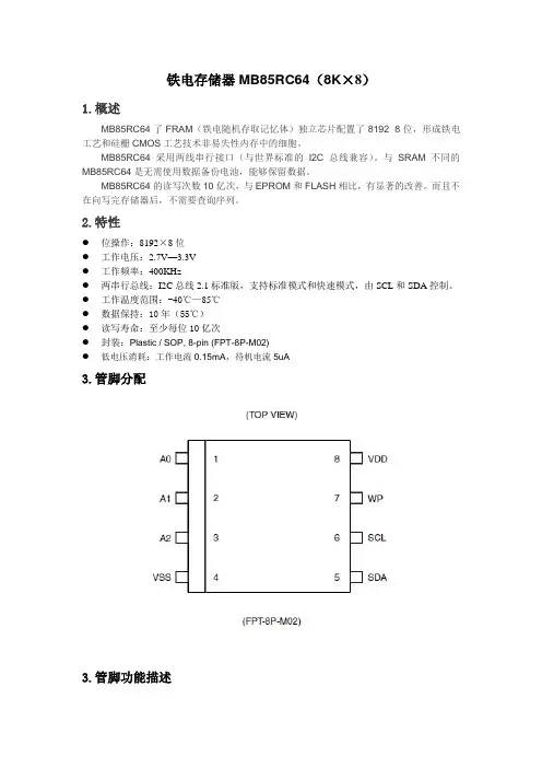
铁电存储器MB85RC64(8K×8)1.概述MB85RC64了FRAM(铁电随机存取记忆体)独立芯片配置了8192×8位,形成铁电工艺和硅栅CMOS工艺技术非易失性内存中的细胞。
MB85RC64采用两线串行接口(与世界标准的I2C总线兼容)。
与SRAM不同的MB85RC64是无需使用数据备份电池,能够保留数据。
MB85RC64的读写次数10亿次,与EPROM和FLASH相比,有显著的改善。
而且不在向写完存储器后,不需要查询序列。
2.特性●位操作:8192×8位●工作电压:2.7V—3.3V●工作频率:400KHz●两串行总线:I2C总线2.1标准版,支持标准模式和快速模式,由SCL和SDA控制。
●工作温度范围:-40℃—85℃●数据保持:10年(55℃)●读写寿命:至少每位10亿次●封装:Plastic / SOP, 8-pin (FPT-8P-M02)●低电压消耗:工作电流0.15mA,待机电流5uA3.管脚分配3.管脚功能描述管教编号管脚名功能描述1—3 A0/A1/A2 器件地址一个I2C总线可以连接8个和MB85RC64类似的器件。
通过将A0/A1/A2与VDD和VSS连接,确定每个器件的地址。
如果A0/A1/A2未连接,默认为0。
CPU通过SDA线输出一个地址与器件进行匹配。
4 VSS 数字地5 SDA 数据IO串口这是双向通信的数据IO口,用来读写铁电存储器的阵列数据,这是开漏极输出,可能是与其它漏极开路(或者集电极开路信号总线)进行线或运算,因此需要一个上拉电阻连接到外部电路。
6 SCL 时钟串口这是时钟输入口,时钟上升沿进行数据采样,下降沿进行数据输出。
7 WP 写保护WP是H电平,禁止写入。
WP是L电平,可进行写数据,如果WP没有置位,默认为L电平。
而读数据操作,不受WP 管脚的限制。
8 VDD 电源电压4.模块框图5.I2C电路MB85RC64有两线串行接口,支持I2C总线,并作为从器件工作。
如何申请样片做项目常常避免不了申请样片,原因无外这几种情况:一是芯片不好买;二是太贵而又最小定量限制。
几个建议,一是要有正当用途,不要以为是免费午餐就滥申请;二是一般使用公司或学校等较为正式的邮箱申请。
1、ADI,需要注册成会员。
2、TI,也比较大方,会有人工审核,甚至会电话过来问一些问题。
如果申请数量过多,太贵,有可能被视为恶意申请而进入黑名单。
不过有申辩的机会,我一哥们被判为恶意申请后又邮件投诉依然申请成功,另一哥们两次申请10片INA128被直接电话质疑。
半年有6次申请机会,用完后不可申请。
注:我们实验室用MSP430比较多,TI的样片申请给我的感觉还是很不错的。
3、Microchip,速度很慢,有时候要自己到代理商那里去取。
可以申请,样片种类限制不多。
4、Maxim,就不用说了,公认的最容易申请的,就是快递速度较慢,普通包裹,北京发货。
5、Intersil,速度一般,限制不多,也没有特殊要求,也很大方。
6、Linear,速度很快,没什么限制,它的电源管理芯片很好用。
北京或香港发货。
7、WCH,国内的,南京沁恒电子,一次一片,以前是挂号,现在是自付邮资(快递),本人曾认真委婉地投诉过他们的客服。
注:这家的片子我没用过。
8、Cypress,赛普拉斯,也很大方,甚至连评估板都提供申请。
我兄弟申请过,没有亲自尝试。
9、Onsemi,安森美,专业搞电源管理的。
样片申请交给代理商了,比如武汉力源,对于武汉力源(icbase)的评价还是不错的。
10、Cirrus Logic ,样片申请是摆设,至少对于我的正式申请没有任何回音。
好在当时没有等待Cirrus Logic ,直接换成ADI的器件了。
11、NXP,恩智浦半导体,据说不太好申请,但其产品应用很广泛。
另一篇:1、(推荐)南京沁恒电子有限公司 USB芯片比较爽 CH375A/technique/index2.asp免费申请 USB 芯片 CH375南京沁恒公司首页:/index.asp申请网址:/technique/index2.asp2、(推荐)飞思卡尔免费样品申请/webapp/sps/site/homepage.jsp?nodeId=010984007869597059 2869294893、(推荐) 申请了10多次都收到了,一次能申请三种,每种两片的限制。
带R TC的I2C总线铁电存储器FM31256■中南大学 陈淼 凌玉华 廖力清 摘 要FM31256是一种基于I2C总线、采用铁电体技术的多功能存储芯片。
除了非易失存储器外,该器件还具有实时时钟、低电压复位、看门狗计数器、非易失性事件计数器、可锁定的串行数字标识等多种功能。
文章主要介绍了FM31256的基本功能、原理,并结合实例给出了其在电磁铸轧电源控制装置中的具体应用方法。
关键词I2C总线 铁电体技术 R TC MSP430F FM31256是由Ramtron公司推出的新一代多功能系统监控和非易失性铁电存储芯片。
与其他非易失性存储器比较,它具有如下优点:读/写速度快,没有写等待时间;功耗低,静态电流小于1mA,写入电流小于150mA;擦写使用寿命长,芯片的擦写次数为100亿次,比一般的EEPROM存储器高10万倍,即使每秒读/写30次,也能用10年;读/写的无限性,芯片擦写次数超过100亿次后,还能和SRAM一样读/写。
铁电存储器(FRAM)的核心技术是铁电晶体材料。
这一特殊材料使铁电存储器同时拥有随机存取存储器(RAM)和非易失性存储的特性。
本文介绍了FM31256的主要功能,并具体给出了基于嵌入式C语言编写的存储器读/写程序。
1 FM31256的基本结构及原理FM31256由256K B存储器和处理器配套电路(pro2 cessor companion)两部分组成。
与一般的采用备份电池保存数据不同,FM31256是真正意义上的非易失(truly nonvolatile)存储器,并且用户可以选择对不同的存储区域以软件方式进行写保护。
FM31256器件将非易失FRAM与实时时钟(R TC)、处理器监控器、非易失性事件计数器、可编程可锁定的64位ID号和通用比较器相结合。
其中,通用比较器可提前在电源故障中断(NMI)时发挥作用或实现其他用途。
采用先进的0.35μm制造工艺,这些功能通过一个通用接口嵌入到14个引脚的SOIC封装中,从而取代系统板上的多个元件。
FRAM 常见问题解答1. 什么是 FRAM?FRAM 是 ferroelectric random access memory(铁电随机存取存储器)的首字母缩写,它是非易失性存储器,即便在断电后也能保留数据。
尽管从名称上说,FRAM 是铁电存储器,但它不受磁场的影响,因为芯片中不含铁基材料(铁)。
铁电材料可在电场中切换极性,但是它们不受磁场的影响。
2. FRAM 较之闪存/EEPROM 具有哪些主要优势?1) 速度。
FRAM 具有快速写入的特性。
写入到 FRAM 存储器单元的实际时间小于50ns,这超越了所有其他存储器的类似操作。
这大约比 EEPROM 快 1000 倍。
此外,与需要两步(写入命令和随后的读取/验证命令)才能写入数据的EEPROM 不同,FRAM 的写入操作与读取操作发生在同一过程中。
只提供一个存储器访问命令,实现读取或写入功能。
因此,与 EEPROM 写入处理相关联的所有时间实际上在基于 FRAM 的智能 IC 中被有效地消除了。
2) 低功耗。
在低电压下写入 FRAM 单元,并且只需很低的电流即可更改数据。
对于 EEPROM,则需要高电压。
FRAM 使用非常低的电源电压----1.5V,而 EEPROM 则使用 10-14V 电源电压。
FRAM 的低电压意味着低功耗,同时能够在更快的处理速度下实现更多功能。
3) 数据可靠性。
由于只需要少量能量,因此操作FRAM所需的所有能量在数据写入开始时就被预先加载。
这就避免了“数据分裂” —由于能源缺乏的关系导致部分数据在写入时被破坏。
基于 EEPROM 的智能 IC 在写周期内被从射频(RF) 磁场电源中移除时就会出现这种情况。
此外,FRAM 还具有 100 兆次的写入/读取数或更多 ---- 远远超过了EEPROM 的写入数量。
3. FRAM 在高温环境下的表现如何?FRAM 是一项非常强大可靠的存储技术,即使在高温环境下也是如此。
带RTC(Real-Time Clock)的I2C总线铁电存储器FM31256 内容摘要:FM31256是一种基于I2C总线、采用铁电体技术的多功能存储芯片。
除了非易失存储器外,该器件还具有实时时钟、低电压复位、看门狗计数器、非易失性事件计数器、可锁定的串行数字标识等多种功能。
文章主要介绍了FM31256的基本功能、原理,并结合实例给出了其在电磁铸轧电源控制装置中的具体应用方法。
FM31256是由Ramtron公司推出的新一代多功能系统监控和非易失性铁电存储芯片。
与其他非易失性存储器比较,它具有如下优点:读/写速度快,没有写等待时间;功耗低,静态电流小于1 mA,写入电流小于150 mA;擦写使用寿命长,芯片的擦写次数为100亿次,比一般的EEPROM存储器高10万倍,即使每秒读/写30次,也能用10年;读/写的无限性,芯片擦写次数超过100亿次后,还能和SRAM一样读/写。
铁电存储器(FRAM)的核心技术是铁电晶体材料。
这一特殊材料使铁电存储器同时拥有随机存取存储器(RAM)和非易失性存储的特性。
本文介绍了FM31256的主要功能,并具体给出了基于嵌入式C语言编写的存储器读/写程序。
1FM31256的基本结构及原理FM31256由256 KB存储器和处理器配套电路(processor companion)两部分组成。
与一般的采用备份电池保存数据不同,FM31256是真正意义上的非易失(truly nonvolatile)存储器,并且用户可以选择对不同的存储区域以软件方式进行写保护。
FM31256 器件将非易失FRAM与实时时钟(RTC)、处理器监控器、非易失性事件计数器、可编程可锁定的64位ID号和通用比较器相结合。
其中,通用比较器可提前在电源故障中断(NMI)时发挥作用或实现其他用途。
采用先进的0.35 μm制造工艺,这些功能通过一个通用接口嵌入到14个引脚的SOIC封装中,从而取代系统板上的多个元件。
1n R O B O T SSelection Guide Edition 19 • Revised April 1, 20192.Pose repeatability details can be found in the product manual.3.The value with the movements and conditions below when the MvTune2 (high-speed movement mode) is applied.4.The values in parentheses are the values when the large inertia mode is enabled.5.When the maximum load is installed, the downward pushing force generated at the tip of the load is obtained with J1, J2, and J4 axes stopped. The force shown above is the maximum value. When the force is applied for a long time, an overload error will be generated.6.The values in parentheses are the values when the large inertia mode is enabled.7.The protection specification details can be found in the product manual.8.Sets the robot’s operating environmental temperature as parameter OLTMX. Corresponding to the environment, the continuous control action performance and the overload-protection function are optimized. (Refers to product manual for details.)RHCH SeriesF Series RobotsMust select items 1–4.Mitsubishi Electric Automation | Robots 2Selection Guide Edition 19 • Revised April 1, 20192.Pose repeatability details can be found in the product manual.3.The value with the movements and conditions below when the MvTune2 (high-speed movement mode) is applied.4.The values in parentheses are the values when the large inertia mode is enabled.5.When the maximum load is installed, the downward pushing force generated at the tip of the load is obtained with J1, J2, and J4 axes stopped. The force shown above is the maximum value. When the force is applied for a long time, an overload error will be generated.6.The values in parentheses are the values when the large inertia mode is enabled.7.The protection specification details can be found in the product manual.8.Sets the robot’s operating environmental temperature as parameter OLTMX. Corresponding to the environment, the continuous control action performance and the overload-protection function are optimized. (Refers to “product manual for details.)F Series Robots。
什么是铁电存储器?相对于其它类型的半导体技术而言,铁电存储器具有一些独一无二的特性。
传统的主流半导体存储器可以分为两类--易失性和非易失性。
易失性的存储器包括静态存储器SRAM(static random access memory)和动态存储器DRAM (dynamic random access memory)。
SRAM和DRAM在掉电的时候均会失去保存的数据。
RAM 类型的存储器易于使用、性能好,可是它们同样会在掉电的情况下会失去所保存的数据。
非易失性存储器在掉电的情况下并不会丢失所存储的数据。
然而所有的主流的非易失性存储器均源自于只读存储器(ROM)技术。
正如你所猜想的一样,被称为只读存储器的东西肯定不容易进行写入操作,而事实上是根本不能写入。
所有由ROM技术研发出的存储器则都具有写入信息困难的特点。
这些技术包括有EPROM (几乎已经废止)、EEPROM和Flash。
这些存储器不仅写入速度慢,而且只能有限次的擦写,写入时功耗大。
铁电存储器能兼容RAM的一切功能,并且和ROM技术一样,是一种非易失性的存储器。
铁电存储器在这两类存储类型间搭起了一座跨越沟壑的桥梁--一种非易失性的RAM。
美国Ramtron公司铁电存储器(FRAM)的核心技术是铁电晶体材料。
这一特殊材料使铁电存储器同时拥有随机存取记忆体(RAM)和非易失性存储器的特性。
铁电晶体的工作原理是:当在铁电晶体材料上加入电场,晶体中的中心原子会沿着电场方向运动,达到稳定状态。
晶体中的每个自由浮动的中心原子只有2个稳定状态,一个记为逻辑中的0,另一个记为1。
中心原子能在常温、没有电场的情况下,停留在此状态达100年以上。
铁电存储器不需要定时刷新,能在断电情况下保存数据。
由于整个物理过程中没有任何原子碰撞,铁电存储器有高速读写、超低功耗和无限次写入等特性。
铁电存储器和E2PROM比较起来,主要有以下优点:(1)FRAM可以以总线速度写入数据,而且在写入后不需要任何延时等待,而E2PROM在写入后一般要5~10 ms的等待数据写入时间;(2)FRAM有近乎无限次写入寿命。
谈到存储器,许多人经常被众多的缩写词弄得一头雾水,难以理解各类存储器在技术本质上的差异,因此在正式说明新兴存储器之前,笔者将先提供一些基础说明。
存储器的分类概念先就概念部分来说明。
存储器在应用范畴、用量规模等空间角度来看可分成2类,即主流与利基,如DDR2 SDRAM、GDD3 SDRAM 等的用量、产量极大,运用也普及,因此属主流存储器;相对的,仅在些许领域使用或用量偏少的存储器则为利基存储器,如串列式E EPROM、NV SRAM等多只用在嵌入式应用,因此属于利基型。
再就时间角度看,也可分成2类:新兴存储器与过时存储器,新兴存储器例如FRAM、MRAM等,过时存储器则是过去存在,但之后被其他类型存储器所取代,进而走入历史的存储器,例如EPROM被EEPROM或Flash Memory所取代,或如磁环存储器(Magnetic core memory)被DRAM所取代,以及磁泡存储器(Bubble memory)被硬碟所取代等等。
6种技术变化层次接着是存储器技术变化层次的不同,笔者归纳分析后认为可以分成6个层次,储存原理的不同、储存结构的不同、存取结构的不同、制程技术的不同、模组设计的不同、以及模组构型的不同。
所谓「储存原理的不同」,即是从最根基的位元记忆方式就有差别,DRAM将位元值储存于电容内,而SRAM将位元资料存于电晶体内,或如FRAM使用铁电效应来储存位元,MRAM使用磁阻原理来储存位元。
再来是「储存结构的不同」,同样是运用电容来储存0、1的位元值,Z-RAM的作法就与DRAM不同,DRAM在晶圆电路设计时会为每个位元设置一个电容,但Z-RAM直接倚赖硅绝缘(Silicon on insulator;SOI)基板所造成的浮体效应(Floating body effect)来充当电容,虽然结构作法不同,但原理仍相同。
类似的,4T SRAM、6T SRAM、乃至8T SRAM,基本上都是将0、1资料存于电晶体内,只是构成每个记忆格(Cell)所用的电晶体数不同(T即指Transistor)。
This data sheet contains design specifications for product development. Ramtron International Corporation These specifications may change in any manner without notice 1850 Ramtron Drive, Colorado Springs, CO 80921 FM250404Kb FRAM Serial MemoryFeatures4K bit Ferroelectric Nonvolatile RAM • Organized as 512 x 8 bits• High endurance 10 Billion (1010) read/writes • 10 year data retention at 85° C • NoDelay™ write• Advanced high-reliability ferroelectric processFast Serial Peripheral Interface - SPI • Up to 2.1 MHz maximum bus frequency • Direct hardware replacement for EEPROM • Supports SPI Mode 0 (CPOL=0, CPHA=0)Sophisticated Write Protection Scheme • Hardware protection • Software protectionLow Power Consumption • 10 µA standby currentIndustry Standard Configuration• Industrial temperature -40° C to +85° C • 8-pin SOP or DIPDescriptionThe FM25040 is a 4-kilobit nonvolatile memory employing an advanced ferroelectric process. A ferroelectric random access memory or FRAM is nonvolatile but operates in other respects as a RAM. It provides reliable data retention for 10 years while eliminating the complexities, overhead, and system level reliability problems caused by EEPROM and other nonvolatile memories.Unlike serial EEPROMs, the FM25040 performs write operations at bus speed. No write delays are incurred. Data is written to the memory array mere hundreds of nanoseconds after it has been successfully transferred to the device. The next bus cycle may commence immediately. In addition the product offers substantial write endurance compared with other nonvolatile memories. The FM25040 is capable of supporting up to 1E10 read/write cycles -- far more than most systems will require from a serial memory.These capabilities make the FM25040 ideal for nonvolatile memory applications requiring frequent or rapid writes. Examples range from data collection, where the number of write cycles may be critical, to demanding industrial controls where the long write time of EEPROM can cause data loss.The FM25040 provides substantial benefits to users of serial EEPROM, in a hardware drop-in replacement. The FM25040 uses the high-speed SPI bus which enhances the high-speed write capability of FRAM technology. It is guaranteed over an industrial temperature range of -40°C to +85°C.Pin ConfigurationCS SO WP VSSVCC HOLD SCK SIPin Names Function /CS Chip SelectSO Serial Data Output /WP Write Protect VSS GroundSI Serial Data Input SCK Serial Clock /HOLD HoldVCC Supply Voltage 5VOrdering InformationFM25040-P 8-pin plastic DIP FM25040-S8-pin SOPFigure 1. Block DiagramPin DescriptionPin Name Pin Number I/O Pin Description/CS 1 I Chip Select. Activates the device. When high, all outputs are tri-state andthe device ignores other inputs. The part remains in a low power standbymode. When low, the part recognizes activity on the SCK signal. Afalling edge on /CS must occur prior to every op-code.SO 2 O Serial Output. SO is the data output pin. It is driven actively during a readand remains tri-state at all other times including when /HOLD is low.Data transitions are driven on the falling edge of the serial clock.* SO can be connected to SI for a single pin data interface since the partcommunicates in half-duplex fashion./WP 3 I Write Protect. This pin prevents all write operations. If low, the part iscompletely write protected. If high, write access is determined by theother write protection features. A complete explanation of writeprotection is provided below. *Note that the function of /WP is differentfrom the FM25160 where it protects the status register only.VSS 4 I GroundSI 5 I Serial Input. All data is input to the device on this pin. The pin is sampledon the rising edge of SCK and is ignored at other times. It should alwaysbe driven to a valid logic level to meet ICC specifications.* SI may be connected to SO for a single pin data interface.SCK 6 I Serial Clock. All I/O activity is synchronized to the serial clock. Inputsare latched on the rising edge and outputs occur on the falling edge. Thepart is static so the clock frequency may be any value between 0 and 2.1MHz and may be interrupted at any time./HOLD 7 I Hold. The /HOLD signal is used when the host CPU must interrupt amemory operation for another task. Taking the /HOLD signal to a lowstate pauses the current operation. The part ignores any transition on SCKor /CS. All transitions on /HOLD must occur while SCK is low.VCC 8 I Supply Voltage. 5VOverviewThe FM25040 is a serial FRAM memory. The memory array is logically organized as 512 x 8 and is accessed using an industry standard Serial Peripheral Interface or SPI bus. Functional operation of the FRAM is similar to serial EEPROMs. The major difference between the FM25040 and a serial EEPROM with the same pin-out relates to its superior write performance.Memory ArchitectureWhen accessing the FM25040, the user addresses 512 locations each with 8 data bits. These data bits are shifted serially. The addresses are accessed using the SPI protocol, which includes a chip select (to permit multiple devices on the bus), an op-code including the upper address bit, and a word address. The word address consists of the lower 8-addres bits. The complete address of 9-bits specifies each byte address uniquely.Most functions of the FM25040 are either controlled by the SPI interface, or are handled automatically by on-board circuitry. The access time for memory operation essentially is zero, beyond the time needed for the serial protocol. That is, the memory is read or written at the speed of the SPI bus. Unlike an EEPROM, it is not necessary to poll the device for a ready condition since writes occur at bus speed. That is, by the time a new bus transaction can be shifted into the part, a write operation will be complete. This is explained in more detail in the interface section below.Users expect several obvious system benefits from the FM25040 due to its fast write cycle and high endurance as compared with EEPROM. However there are less obvious benefits as well. For example in a high noise environment, the fast-write operation is less susceptible to corruption than an EEPROM since it is completed quickly. By contrast, an EEPROM requiring milliseconds to write is vulnerable to noise during much of the cycle.Note that the FM25040 contains no power management circuits other than a simple internal power-on reset. It is the user’s responsibility to ensure that VCC is within data sheet tolerances to prevent incorrect operation.Serial Peripheral Interface – SPI BusThe FM25040 employs a Serial Peripheral Interface (SPI) bus. This high-speed serial bus provides high performance serial communication with a host microcontroller. Many common microcontrollers have hardware SPI ports allowing a direct interface. It is quite simple to emulate the SPI interface using ordinary port pins for microcontrollers that do not. Note that the FM25040 operates in SPI Mode 0 only. The SPI interface uses a total of four pins; clock, data-in, data-out, and chip select. It is possible to connect the two data lines together. Figure 2 illustrates a typical system configuration using the FM25040 with a microcontroller that offers an SPI port. Figure 3 shows a similar configuration for a microcontroller that has no hardware support for the SPI bus. Protocol OverviewThe SPI interface is a synchronous serial interface using clock and data lines. It is intended to support multiple devices on the bus. Each device is activated using a chip select. Once chip select is activated by the bus master, the FM25040 will begin monitoring the clock and data lines. The relationship between the falling edge of /CS, the clock and data is dictated by the SPI mode. There are four such modes however the FM25040 supports only mode 0. This mode dictates that the SCK signal must be low when /CS is activated.The SPI protocol is controlled by op-codes. These op-codes specify the commands to the part. After /CS is activated, the first byte transferred from the bus master is the op-code. Following the op-code, any addresses and data are then transferred. Certain op-codes are commands with no subsequent data transfer. The /CS must go inactive after an operation is complete and before a new op-code can be issued.Data TransferAll data transfers to and from the FM25040 occur in8-bit groups. They are synchronized to the clocksignal (SCK) and occur most significant bit (MSB)first. Serial inputs are clocked in on the rising edgeof SCK. Outputs are driven on the falling edge ofSCK.Command StructureThere are six commands called op-codes that can beissued by the bus master to the FM25040. They arelisted in the table below. These op-codes control thefunctions performed by the memory. They can bedivided into three categories. First, are commandsthat have no subsequent operands. They perform asingle function such as to enable a write operation.Second are commands followed by one byte, either inor out. They operate on the status register Last arecommands for memory transactions followed byaddress and one or more bytes of data.Table 1. Op-code CommandsName Description Op-code value WREN Set Write Enable Latch 00000110 WRDI Write Disable 00000100 RDSR Read Status Register 00000101 WRSR Write Status Register 00000001 READ Read Memory Data 0000A011 WRITE Write Memory Data0000A010 WREN - Set Write Enable LatchThe FM25040 will power up with writes disabled.The WREN command must be issued prior to anywrite operation. Sending the WREN op-code willallow the user to issue subsequent op-codes for writeoperations. These include writing the status registerand writing the memory. Sending the WREN op-code causes the internal Write Enable Latch to be set. A flag bit in the status register, called WEL, indicates the state of the latch. WEL=1 indicates that writes are permitted. Attempting to write the WEL bit in the status register has no affect. Completing any write operation (rising edge of /CS) will automatically clear the Write Enable Latch and prevent further writes without another WREN command. Figure 4 below illustrates the WREN command bus configuration. WRDI - Write Disable The WRDI command disables all write activity byclearing the Write Enable Latch. The user can verify that writes are disabled by reading the WEL bit in thestatus register and verifying that WEL=0. Figure 5 below illustrates the WRDI command bus configuration.RDSR - Read Status RegisterThe RDSR command allows the bus master to verify the contents of the Status register. Reading Status provides information about the current state of the write protection features. Following the RDSR op-code, the FM25040 will return one bye with the contents of the Status register. The Status register is described in detail in a later section. WRSR – Write Status RegisterThe WRSR command allows the user to select certain write protection features by writing a byte to the Status register. Prior to issuing a WRSR command, the /WP pin must be high or inactive. Note that on the FM25040 /WP prevents writing to the Status register and the memory array. Also prior to sending the WRSR command, the user must send a WREN command to enable writes. Note that executing a WRSR command is a write operation and therefore clears the Write Enable Latch. The bus configuration of RDSR and WRSR are shown below.Status Register & Write ProtectionThe write protection features of the FM25040 are relatively simple to use. First, a WREN op-code must be issued prior to any write operation. Assuming that writes are enabled using WREN, writes to memory are controlled by the /WP pin and the Status register. When /WP is low, the entire part is write protected. When /WP is high, the memory protection is subject to the Status register. As described above, writes to the status register are performed using the WRSR command and are subject to the /WP pin. The Status register is organized as follows.Table 2. Status RegisterBit 7 6 5 4 3 2 1 0 Name 0 0 0 0 BP1 BP0 WEL 0 Bits 0 and 4-7 are fixed at 0 and can not be modified. Note that the Ready bit in many EEPROMs is unnecessary as the FRAM writes in real-time and is never busy. The BP1 and BP0 control write protection features. They are nonvolatile! The WEL flag indicates the state of the Write Enable Latch. Writing the WEL bit in the status register has no affect. BP1 and BP0 are memory block write protection bits. They specify portions of memory that are write protected as shown in the following table.Table 3. Block Memory Write ProtectionBP1 BP0 Protected Address Range0 0 None0 1 180h to 1FFh (upper ¼)1 0 100h to 1FFH (upper ½)1 1 000h to 1FFh (all)The BP1 and BP0 bits protect selected portions of the memory array from writes. The /WP pin and Write Enable Latch protect the entire part including the BP bits. The following table summarizes the write protection conditions.Table 4. Write ProtectionWEL /WP Protected Blocks Unprotected Blocks Status Register0 X Protected Protected Protected1 0 Protected Protected Protected1 1 Protected Unprotected UnprotectedMemory OperationThe SPI interface, with its relatively high maximum clock frequency, highlights the fast write capability of the FRAM technology. Unlike SPI bus EEPROMs the FM25040 can perform sequential writes at bus speed. No page register is needed and any number of sequential writes may be performed.Write OperationAll writes to the memory array begin with a WREN op-code. The bus master then issues a WRITE op-code. Part of this op-code includes the upper bit of the memory address. Bit 3 in the op-code corresponds to A8. The next byte is the lower 8-bits of the address A7-A0. In total, the 9-bits specify the address of the first byte of the write operation. Subsequent bytes are data and they are written sequentially. Addresses are incremented internally as long as the bus master continues to issue clocks. If the last address of 1FFh is reached, the counter will roll over to 000h. Data is written MSB first.Unlike EEPROMs, any number of bytes can be written sequentially and each byte is written to memory immediately after it is clocked in (after the 8th clock) . The rising edge of /CS terminates a WRITE op-code operation. Read OperationAfter the falling edge of /CS, the bus master can issue a READ op-code. Part of this op-code includes the upper bit of the memory address. The next byte is the lower 8-bits of the address. In total, the 9-bits specify the address of the first byte of the read operation. After the op-code is complete, the SI line is ignored. The bus master then issues 8 clocks, with one bit read out for each. Addresses are incremented internally as long as the bus master continues to issue clocks. If the last address of 1FFh is reached, the counter will roll over to 000h. Data is read MSB first. The rising edge of /CS terminates a READ op-code operation.. The bus configuration for read and write operations is shown below.HoldThe /HOLD pin can be used to interrupt a serial operation without aborting it. If the bus master takes the /HOLD pin low while SCK is low, the current operation will pause. Taking the /HOLD pin high while SCK is low will resume an operation. The transitions of /HOLD must occur while SCK is low, but the SCK and I/O pins can toggle during a hold state. However, before removing the HOLD condition, all pins should return to their state prior to the HOLD. A diagram illustrating the HOLD timing is provided in the electrical specifications.Data Retention and EnduranceData retention is specified in the electrical specifications below. For purposes of clarity, this section contrasts the retention and endurance of FRAM with EEPROM. The retention performance of FRAM is very comparable to EEPROM in its characteristics. However, the effect of endurance cycles on retention is different.A typical EEPROM has a write endurance specification that is fixed. Surpassing the specified level of cycles on an EEPROM usually leads to a hard memory failure. By contrast, the effect of increasing cycles on FRAM produces an increase in the soft error rate. That is, there is a higher likelihood of data loss but the memory continues to function properly. A hard failure would not occur by simply exceeding the endurance specification; simply a reduction in data retention reliability. While enough cycles would cause an apparent hard error, this is simply a very high soft error rate. This characteristic makes it problematic to assign a fixed endurance specification. Endurance is a soft specification. Therefore, the user may operate the device with different levels of endurance cycling for different portions of the memory. For example, critical data needing the highest reliability level could be stored in memory locations that receive comparatively few cycles. Data with shorter-term use could be located in an area receiving many more cycles. A scratchpad area, needing little if any retention can be cycled until there is virtually no retention capability remaining. This would occur several orders of magnitude above the endurance spec.Internally, a FRAM operates with a read and restore mechanism similar to a DRAM. Therefore, endurance cycles are applied for each access: read or write. The FRAM architecture is based on an array of rows and columns. Each access causes a cycle for an entire row. Therefore, data locations targeted for substantially differing numbers of cycles should not be located within the same row. In the FM25040, there are 64 rows each 64 bits wide. Each 8 bytes in the address mark the beginning of a new row.ApplicationsThe versatility of FRAM technology fits into many diverse applications. Clearly the strength of higher write endurance and faster writes make FRAM superior to EEPROM in all but one-time programmable applications. The advantage is most obvious in data collection environments where writes are frequent and data must be nonvolatile.The attributes of fast writes and high write endurance combine in many innovative ways. A short list of ideas is provided here.1. Data collection. In applications where data is collected and saved, FRAM provides a superior alternative to other solutions. It is more cost effective than battery backup for SRAM and provides better write attributes than EEPROM.2. Configuration. Any nonvolatile memory can retain a configuration. However if the configuration changes and power failure is a possibility, the higher write endurance of FRAM allows changes to be recorded without restriction. Any time the system state is altered, the change can be written. This avoids writing to memory on power down when the available time is short and power scarce.3. High noise environments. Writing to EEPROM in a noisy environment can be challenging. When severe noise or power fluctuations are present, the long write time of EEPROM creates a window of vulnerability during which the write can be corrupted. The fast write of FRAM is complete within a microsecond. This time is typically too short for noise or power fluctuation to disturb it.4. Time to market. In a complex system, multiple software routines may need to access the nonvolatile memory. In this environment the time delay associated with programming EEPROM adds undue complexity to the software development. Each software routine must wait for complete programming before allowing access to the next routine. When time to market is critical, FRAM can eliminate this simple obstacle. As soon as a write is issued to the FM25040, it is effectively done -- no waiting.5. RF/ID. In the area of contactless memory, FRAM provides an ideal solution. Since RF/ID memory is powered by an RF field, the long programming time and high current consumption needed to write EEPROM is unattractive. FRAM provides a superior solution. The FM25040 is suitable for multi-chip RF/ID products.6. Maintenance tracking. In sophisticated systems, the operating history and system state during a failure is important knowledge. Maintenance can be expedited when this information has been recorded. Due to the high write endurance, FRAM makes an ideal system log. In addition, the convenient 2-wire interface of the FM25040 allows memory to be distributed throughout the system using minimal additional resources.Electrical SpecificationsAbsolute Maximum RatingsDescription RatingsAmbient storage or operating temperature -40°C to + 85°CVoltage on any pin with respect to ground -1.0V to +7.0VD.C. output current on any pin 5 mALead temperature (Soldering, 10 seconds) 300° CStresses above those listed under Absolute Maximum Ratings may cause permanent damage to the device. This is a stress rating only, and the functional operation of the device at these or any other conditions above those listed in the operational section of this specification is not implied. Exposure to absolute maximum ratings conditions for extended periods may affect device reliabilityDC Operating Conditions TA = -40° C to + 85° C, VCC = 4.5V to 5.5V unless otherwise specifiedSymbol Parameter Min Typ Max Units NotesVCC Main Power Supply 4.5 5.0 5.5 V 10.9 1.2 mA 2ICC VCC Supply Current@ SCK = 1.0 MHz1.62.5 mA 2ICC VCC Supply Current@ SCK = 2.1 MHzISB Standby Current 1 10 µA 3ILI Input Leakage Current 10 µA 4ILO Output Leakage Current 10 µA 4VIL Input Low Voltage -0.3 VCC x 0.3 V 1VIH Input High Voltage VCC x 0.7 VCC + 0.5 V 1VOL Output Low Voltage0.4 V 1@ IOL = 2 mAVCC-0.8 V 1VOH Output High Voltage@ IOH = -1 mAVHYS Input Hysteresis VCC x .05 V 1, 5Notes1. Referenced to VSS.2. SCK toggling between VCC-0.3V and VSS, other inputs VSS or VCC-0.3V3. SCK = SI = /CS=VCC. All inputs VSS or VCC.4. VIN or VOUT = VSS to VCC5. This parameter is periodically sampled and not 100% tested.AC Parameters TA = -40° C to + 85° C, VCC = 4.5V to 5.5V unless otherwise specified Symbol Parameter Min Max Units fCK SCK Clock Frequency 0 2.1 MHz tCH Clock High Time 200 nstCL Clock Low Time 200 nstCSU Chip Select Setup 240 nstCSH Chip Select Hold 240 nstOD Output Disable 240 nstODV Output Data Valid 200nstOH Output Hold 0 ns tD Deselect Time 240 ns tR Data Rise Time 2.0 µS tF Data Fall Time 2.0 µS tH Data Hold Time 100 ns tSU Data Setup Time 100 ns tHS /Hold Setup Time 90 ns tHH /Hold Hold Time 90 ns tHZ /Hold Low to Hi-Z 100 ns tLZ /Hold High to Data Active 100 nsNotes1. Rise and fall times measured between 10% and 90% of waveform.Capacitance TA = 25° C , f=1.0 MHz, VCC = 5VSymbol Parameter Max Units NotesCO Output capacitance (SDA) 8 pF 1CI Input capacitance 6 pF 1Notes1. This parameter is periodically sampled and not 100% tested.AC Test ConditionsInput Pulse Levels VCC * 0.1 to VCC * 0.9Input rise and fall times 10 nsInput and output timing levels VCC*0.5Equivalent AC Load CircuitData Retention TA = -40° C to + 85° C, VCC = 4.5V to 5.5V unless otherwise specifiedParameter Min Units NotesData Retention 10 Years 1Notes1. Data retention is specified at 85° C. The relationship between retention, temperature, and the associatedreliability level is characterized separately.Pin 1Index Area.10 mm.004 in.αIndexAreaSelected DimensionsRefer to JEDEC MS-001 for complete dimensions and notes. Controlling dimensions is in inches. Conversions to millimeters are not exact.Symbol Dim Min Nom. MaxA in.mm .210 5.33A1 in.mm 0.015 .381A2 in.mm 0.1152.920.1303.300.1954.95b in.mm 0.014.3560.018.4570.022.508D in.mm 0.3559.020.3659.270.40010.2D1 in.mm 0.005 .127E in.mm 0.3007.620.3107.870.3258.26E1 in.mm 0.2406.100.2506.350.2807.11e in.mm .100 BSC 2.54 BSCeA in.mm .300 BSC 7.62 BSCeB in.mm 0.430 10.92L in.mm 0.1152.920.1303.300.1503.81。