富士通FRAM可以直接替换铁电存储器
- 格式:doc
- 大小:50.50 KB
- 文档页数:2
单片机常用名词解释总线: 指能为多个部件服务的信息传送线,在微机系统中各个部件通过总线相互通信。
地址总线(AB):地址总线是单向的,用于传送地址信息。
地址总线的宽度为16位,因此基外部存储器直接寻址64K,16位地址总线由P0口经地址锁存器提供低8位地址(A0~A7),P2口直接提供高8位地址(A8~A15)。
数据总线(DB):一般为双向,用于CPU与存储器,CPU与外设、或外设与外设之间传送数据信息(包括实际意义的数据和指令码)。
数据总线宽度为8位,由P0口提供。
控制总线(CB):是计算机系统中所有控制信号的总称,在控制总线中传送的是控制信息。
由P3口的第二功能状态和4根独立的控制总线,RESET、EA、ALE、PSEN组成。
存储器:用来存放计算机中的所有信息:包括程序、原始数据、运算的中间结果及最终结果等。
只读存储器(ROM):只读存储器在使用时,只能读出而不能写入,断电后ROM中的信息不会丢失。
因此一般用来存放一些固定程序,如监控程序、子程序、字库及数据表等。
ROM按存储信息的方法又可分为以下几种1、掩膜ROM:掩膜ROM也称固定ROM,它是由厂家编好程序写入ROM(称固化)供用户使用,用户不能更改内部程序,其特点是价格便宜。
2、可编程的只读存储器(PROM):它的内容可由用户根据自已所编程序一次性写入,一旦写入,只能读出,而不能再进行更改,这类存储器现在也称为OTP(Only Time Programmable)。
3、可改写的只读存储器EPROM:前两种ROM只能进行一次性写入,因而用户较少使用,目前较为流行的ROM芯片为EPROM。
因为它的内容可以通过紫外线照射而彻底擦除,擦除后又可重新写入新的程序。
4、可电改写只读存储器(EEPROM): EEPROM可用电的方法写入和清除其内容,其编程电压和清除电压均与微机CPU的5V工作电压相同,不需另加电压。
它既有与RAM一样读写操作简便,又有数据不会因掉电而丢失的优点,因而使用极为方便。
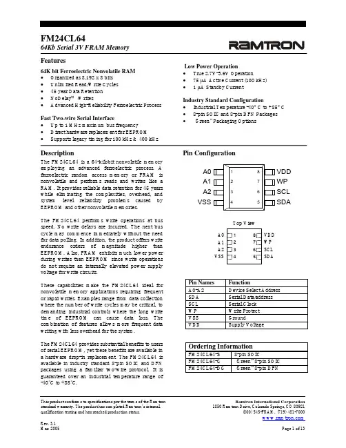
This product conforms to specifications per the terms of the Ramtron Ramtron International Corporationstandard warranty. The product has completed Ramtron’s internal1850 Ramtron Drive, Colorado Springs, CO 80921qualification testing and has reached production status. (800) 545-FRAM, (719) 481-7000FM24CL6464Kb Serial 3V FRAM MemoryFeatures64K bit Ferroelectric Nonvolatile RAM • Organized as 8,192 x 8 bits • Unlimited Read/Write Cycles • 45 year Data Retention • NoDelay™ Writes• Advanced High-Reliability Ferroelectric ProcessFast Two-wire Serial Interface• Up to 1 MHz maximum bus frequency • Direct hardware replacement for EEPROM • Supports legacy timing for 100 kHz & 400 kHzLow Power Operation• True 2.7V-3.6V Operation• 75 µA Active Current (100 kHz) • 1 µA Standby CurrentIndustry Standard Configuration• Industrial Temperature -40° C to +85° C • 8-pin SOIC and 8-pin DFN Packages • “Green” Packaging OptionsDescriptionThe FM24CL64 is a 64-kilobit nonvolatile memory employing an advanced ferroelectric process. A ferroelectric random access memory or FRAM is nonvolatile and performs reads and writes like a RAM. It provides reliable data retention for 45 years while eliminating the complexities, overhead, and system level reliability problems caused by EEPROM and other nonvolatile memories.The FM24CL64 performs write operations at bus speed. No write delays are incurred. The next bus cycle may commence immediately without the need for data polling. In addition, the product offers write endurance orders of magnitude higher than EEPROM. Also, FRAM exhibits much lower power during writes than EEPROM since write operations do not require an internally elevated power supply voltage for write circuits.These capabilities make the FM24CL64 ideal for nonvolatile memory applications requiring frequent or rapid writes. Examples range from data collection where the number of write cycles may be critical, to demanding industrial controls where the long write time of EEPROM can cause data loss. The combination of features allows more frequent data writing with less overhead for the system.The FM24CL64 provides substantial benefits to users of serial EEPROM, yet these benefits are available in a hardware drop-in replacement. The FM24CL64 is available in industry standard 8-pin SOIC and DFN packages using a familiar two-wire protocol. It is guaranteed over an industrial temperature range of -40°C to +85°C.Pin ConfigurationA0A1A2VSSVDD WP SCL SDAPin Names FunctionA0-A2 Device Select Address SDA Serial Data/address SCL Serial Clock WP Write Protect VSS Ground VDD Supply VoltageOrdering InformationFM24CL64-S 8-pin SOIC FM24CL64-G “Green” 8-pin SOIC FM24CL64-DG “Green” 8-pin DFNA0 A1 A2 VSSVDD WP SCL SDAFigure 1. FM24CL64 Block DiagramPin DescriptionPin Name Type Pin DescriptionA0-A2 Input Address 0-2. These pins are used to select one of up to 8 devices of the same type onthe same two-wire bus. To select the device, the address value on the three pins mustmatch the corresponding bits contained in the device address. The address pins arepulled down internally.SDA I/O Serial Data Address. This is a bi-directional line for the two-wire interface. It isopen-drain and is intended to be wire-OR’d with other devices on the two-wire bus.The input buffer incorporates a Schmitt trigger for noise immunity and the outputdriver includes slope control for falling edges. A pull-up resistor is required.SCL Input Serial Clock. The serial clock line for the two-wire interface. Data is clocked out ofthe part on the falling edge, and in on the rising edge. The SCL input alsoincorporates a Schmitt trigger input for noise immunity.WP Input Write Protect. When tied to VDD, addresses in the entire memory map will be write-protected. When WP is connected to ground, all addresses may be written. This pinis pulled down internally.VDD Supply Supply Voltage: 2.7V to 3.6VGroundVSS Supply1010A2A1A0R/W Slave ID Device Select7654321Figure 4. Slave AddressAddressing OverviewAfter the FM24CL64 (as receiver) acknowledges the device address, the master can place the memory address on the bus for a write operation. The address requires two bytes. The first is the MSB. Since the device uses only 13 address bits, the value of the upper three bits are “don’t care”. Following the MSB is the LSB with the remaining eight address bits. The address value is latched internally. Each access causes the latched address value to be incremented automatically. The current address is the value that is held in the latch -- either a newly written value or the address following the last access. The current address will be held for as long as power remains or until a new value is written. Reads always use the current address. A random read address can be loaded by beginning a write operation as explained below.After transmission of each data byte, just prior to the acknowledge, the FM24CL64 increments the internal address latch. This allows the next sequential byte to be accessed with no additional addressing. After the last address (1FFFh) is reached, the address latch will roll over to 0000h. There is no limit to the number of bytes that can be accessed with a single read or write operation.Data TransferAfter the address information has been transmitted, data transfer between the bus master and the FM24CL64 can begin. For a read operation the FM24CL64 will place 8 data bits on the bus then wait for an acknowledge from the master. If the acknowledge occurs, the FM24CL64 will transfer the next sequential byte. If the acknowledge is not sent, the FM24CL64 will end the read operation. For a write operation, the FM24CL64 will accept 8 data bits from the master then send an acknowledge. All data transfer occurs MSB (most significant bit) first.Memory OperationThe FM24CL64 is designed to operate in a manner very similar to other 2-wire interface memory products. The major differences result from the higher performance write capability of FRAM technology. These improvements result in some differences between the FM24CL64 and a similar configuration EEPROM during writes. The complete operation for both writes and reads is explained below.Write OperationAll writes begin with a device address, then a memory address. The bus master indicates a write operation by setting the LSB of the device address to a 0. After addressing, the bus master sends each byte of data to the memory and the memory generates an acknowledge condition. Any number of sequential bytes may be written. If the end of the address range is reached internally, the address counter will wrap from 1FFFh to 0000h.Unlike other nonvolatile memory technologies, there is no effective write delay with FRAM. Since the read and write access times of the underlying memory are the same, the user experiences no delay through the bus. The entire memory cycle occurs in less time than a single bus clock. Therefore, any operation including read or write can occur immediately following a write. Acknowledge polling, a technique used with EEPROMs to determine if a write is complete is unnecessary and will always return a ready condition.Internally, an actual memory write occurs after the 8th data bit is transferred. It will be complete before the acknowledge is sent. Therefore, if the user desires to abort a write without altering the memory contents, this should be done using start or stop condition prior to the 8th data bit. The FM24CL64 uses no page buffering.The memory array can be write protected using the WP pin. Setting the WP pin to a high condition (V DD ) will write-protect all addresses. The FM24CL64 will not acknowledge data bytes that are written to protected addresses. In addition, the address counter will not increment if writes are attempted to these addresses. Setting WP to a low state (V SS ) will deactivate this feature. WP is pulled down internally.Figure 5 below illustrates both a single-byte and multiple-write.。
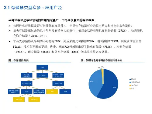

变存储器阻变材料概述本评论文旨在对电阻式随机存取存储器(RRAM)的最新进展进行全面审查。
首先,简单介绍阻变存储器的结构特点以及工作方式。
第二,对RRAM使用的无机阻变材料和有机阻变材料进行了总结,并且它们各自的优点和缺点进行了讨论。
第三,着重介绍无机阻变材料中过渡金属二元氧化物和固态电解质,并展开介绍几种二元氧化物重要的开关机制。
第四,介绍有机阻变材料的组成和应用方向。
第五,介绍电极材料,对电极材料进行分类,介绍不同类型电极材料的特点及应用范围。
第六,对RRAM在非常规的计算以及逻辑器件和多功能RRAMs的应用前景,进行全面总结和彻底讨论。
关键字:阻变存储器,无机阻变材料,有机阻变材料,电极材料第一章绪论自 1947 年贝尔实验室的 Shockley,Brattain 和 Bardeen 发明了第一个锗点接触式晶体管[1],电子产业就从真空电子时代进入了微电子时代。
微电子技术是当代电子信息技术的核心,在国民经济和国家战略上发挥着重要影响。
在技术和需求的驱动下,集成电路从二十世纪六十年代的“小规模集成”发展到现在的“超大/极大规模集成”。
作为微电子技术的重要组成部分,半导体存储器技术也到了迅速的发展,一直朝着“更高密度,更快速度,更低功耗”的方向发展。
如今,存储技术在快速的发展导致电脑在性能和移动应用两个方面的飞速进步,特别是发展固态记忆存储技术,他将是计算机模拟和电子消费类产品市场取得进步的关键因素。
今天,主要的存储器技术是镝动力学随机存取存储器(DRAM)和闪存。
前者,表现出极高的使用寿命和快速的读写速度。
但是,他是一个随机存取存储器,由于受电容充放电的限制只能将数据保持很短的一段时间。
闪存,作为一种主流的非易失性存储器技术,具有良好的收缩性,他理论上可以缩小到32纳米节点。
但是,闪存的写入和访问速度相对缓慢,使用寿命也受到限制。
因此,结合非挥发性高耐力和超越32纳米节点的可扩展性两方面展开了一种新的存储理念的研究。


存储器的存储原理存储器:用来存放计算机中的所有信息:包括程序、原始数据、运算的中间结果及最终结果等。
只读存储器(ROM):只读存储器在使用时,只能读出而不能写入,断电后ROM 中的信息不会丢失。
因此一般用来存放一些固定程序,如监控程序、子程序、字库及数据表等。
ROM按存储信息的方法又可分为以下几种:1、掩膜ROM:掩膜ROM也称固定ROM,它是由厂家编好程序写入ROM(称固化)供用户使用,用户不能更改内部程序,其特点是价格便宜。
2、可编程的只读存储器(PROM):它的内容可由用户根据自已所编程序一次性写入,一旦写入,只能读出,而不能再进行更改,这类存储器现在也称为OTP(Only Time Programmable)。
3、可改写的只读存储器EPROM:前两种ROM只能进行一次性写入,因而用户较少使用,目前较为流行的ROM芯片为EPROM。
因为它的内容可以通过紫外线照射而彻底擦除,擦除后又可重新写入新的程序。
4、可电改写只读存储器(EEPROM):EEPROM可用电的方法写入和清除其内容,其编程电压和清除电压均与微机CPU 的5V工作电压相同,不需另加电压。
它既有与RAM一样读写操作简便,又有数据不会因掉电而丢失的优点,因而使用极为方便。
现在这种存储器的使用最为广泛。
随机存储器(RAM):这种存储器又叫读写存储器。
它不仅能读取存放在存储单元中的数据,还能随时写入新的数据,写入后原来的数据就丢失了。
断电后RAM中的信息全部丢失。
因些,RAM常用于存放经常要改变的程序或中间计算结果等信息。
RAM按照存储信息的方式,又可分为静态和动态两种。
1、静态SRAM:其特点是只要有电源加于存储器,数据就能长期保存。
2、动态DRAM:写入的信息只能保存若干ms时间,因此,每隔一定时间必须重新写入一次,以保持原来的信息不变。
可现场改写的非易失性存储器:这种存储器的特点是:从原理上看,它们属于ROM型存储器,从功能上看,它们又可以随时改写信息,作用又相当于RAM。
谈到存储器,许多人经常被众多的缩写词弄得一头雾水,难以理解各类存储器在技术本质上的差异,因此在正式说明新兴存储器之前,笔者将先提供一些基础说明。
存储器的分类概念先就概念部分来说明。
存储器在应用范畴、用量规模等空间角度来看可分成2类,即主流与利基,如DDR2 SDRAM、GDD3 SDRAM 等的用量、产量极大,运用也普及,因此属主流存储器;相对的,仅在些许领域使用或用量偏少的存储器则为利基存储器,如串列式E EPROM、NV SRAM等多只用在嵌入式应用,因此属于利基型。
再就时间角度看,也可分成2类:新兴存储器与过时存储器,新兴存储器例如FRAM、MRAM等,过时存储器则是过去存在,但之后被其他类型存储器所取代,进而走入历史的存储器,例如EPROM被EEPROM或Flash Memory所取代,或如磁环存储器(Magnetic core memory)被DRAM所取代,以及磁泡存储器(Bubble memory)被硬碟所取代等等。
6种技术变化层次接着是存储器技术变化层次的不同,笔者归纳分析后认为可以分成6个层次,储存原理的不同、储存结构的不同、存取结构的不同、制程技术的不同、模组设计的不同、以及模组构型的不同。
所谓「储存原理的不同」,即是从最根基的位元记忆方式就有差别,DRAM将位元值储存于电容内,而SRAM将位元资料存于电晶体内,或如FRAM使用铁电效应来储存位元,MRAM使用磁阻原理来储存位元。
再来是「储存结构的不同」,同样是运用电容来储存0、1的位元值,Z-RAM的作法就与DRAM不同,DRAM在晶圆电路设计时会为每个位元设置一个电容,但Z-RAM直接倚赖硅绝缘(Silicon on insulator;SOI)基板所造成的浮体效应(Floating body effect)来充当电容,虽然结构作法不同,但原理仍相同。
类似的,4T SRAM、6T SRAM、乃至8T SRAM,基本上都是将0、1资料存于电晶体内,只是构成每个记忆格(Cell)所用的电晶体数不同(T即指Transistor)。