Low-energy electronic structure in Y1-xCaxBa2Cu3O7-y comparison of t ime-resolved optical s
- 格式:pdf
- 大小:170.35 KB
- 文档页数:9

Bluetooth Low EnergyProduct Brief v2.0OverviewBluetooth version 4.0 introduced Bluetooth with low energy functionality. Bluetooth low energy technology allows for short bursts of long-range radio connections, making it ideal for applications that depend on long battery life and don’t need high throughput streaming data. Developers are now able to create sensors that can run on coin-cell batteries for months and even years. Bluetooth low energy technology is built on an entirely new development framework using GATT (Generic Attributes). Silicon Labs supports the latest version of the Bluetooth® Core Specification, Bluetooth™ LE 5.3. We currently do not support all 5.3 features, but we support all the errata published on 5.2 which is mandatory for 5.3 qualification. This enables customers to claim compliance with the latest Bluetooth spec.Bluetooth Low Energy ArchitectureThe Bluetooth Low Energy architecture components are as follows: Physical Layer: Controls radio transmission/receiving.Link Layer: Defines packet structure, includes the state machine and radio control, and provides link layer-level encryption.HCI: A Host-to-Controller interface (HCI) standardizes communication between the controller and the host.L2CAP: Logical Link Control and Adaptation Protocol acts as a protocol multiplexer and handles segmentation and reassembly of packets. ATT: Attribute protocol provides means to transmit data between Bluetooth low energy devices.SM: Security Manager provides means for bonding devices, encrypting and decrypting data, and enabling device privacyGAP: Generic Access Profile layer provides means for Bluetooth low energy devices to advertise themselves or other devices, make device discovery, open and manage connections, and broadcast data.GATT: GATT is used to group individual attributes into logical services GATT also provides information about the attributes, that is, how they can be accessed and what security level is needed.Key Features of Silicon Labs Bluetooth Low Energy StackFeature BenefitCore FeaturesDirection finding, Periodic Advertising with Responses (PAwR), Encrypted Advertising Data (EAD),Advertisement Extensions, Periodic Advertising, LE secure connections, 2M PHY , Long Range, AFH, LE Privacy 1.2 (peripheral), LE packet length extensions, Accept List (central side), GATT, & GATT Caching Scalable AoA Scale to AoA to few hundred devices simultaneouslyCertificate Based Authentication and Pairing (CBAP) Use certificates to authenticate devices before provisioning, thus saving cost and time. Also, prevents counterfeit devices from being provisioned into the networkSilicon Labs Bluetooth stack supports three modes:Standalone mode: Bluetooth stack and the application run in an EFR32SoC or moduleNetwork Co-Processor mode: Bluetooth stack runs on the EFR32, and the application runs on a separate host MCU. API is exposed over a serial interface such as UART.Radio Co-Processor mode: Link layer of the Bluetooth stack runs on the EFR32, and the Host Layer of the stack, as well as the application runs on a separate host MCU or PC. Link Layer and Host Layer communicate via HCI.Technical ResourcesBluetooth Low Energy xG24 Technical Library Data Sheets, App Notes, and moreBluetooth Low Energy xG21 Technical Library Data Sheets, App Notes, and moreBluetooth Low Energy xG22 Technical Library Data Sheets, App Notes, and moreBluetooth Low Energy API Documentation Bluetooth Low Energy API documentationSilicon Labs’ Bluetooth Low Energy HW supportHigh Performance device for Bluetooth LE and Bluetooth mesh applications thatrequire advance features and more Flash and RAMIndustry-leading, energyefficient device for Bluetooth LE applicationsOptimized for line-powered devices including LED bulbs, and gateways for Bluetooth LE and Bluetooth mesh• 1536kB Flash • 256kB RAM • TX power 19.5dBm • -105.7dBm @ 125kbps • -97.6dBm @ 1Mbit/s • -94.8dBm @ 2Mbit/s • RX current 4.4mA @ 1Mbps • TX current 5.0mA @ 0dBm • 1.3 µA Sleep current (16kB ) • Robust peripheral set • AI/ML hardware accelerator • Secure Vault High • QFN40 5x5 (26) •QFN48 6x6 (32)• 512kB Flash • 32kB RAM • TX power 6dBm • -106.7dBm @ 125kbps • -98.9dBm @ 1Mbit/s • -96.2dBm @ 2Mbit/s • RX current 3.6mA @ 1Mbps • TX current 4.1mA @ 0dBm • 1.26µA Sleep current (16kB ) • Lowest Power Bluetooth LE • Secure Vault Mid • QFN40 5x5 (26) • QFN32 4x4 (18) •TQFN32 4x4 (18)• 1024kB Flash • 96kB RAM • TX power 20dBm • -104.9dBm @ 125kbps • -97.5dBm @ 1Mbit/s • -94.4dBm @ 2Mbit/s • RX current 8.8mA @ 1Mbps • TX current 9.3mA @ 0dBm • +135 Junction Temperature • Secure Vault High • Line-Powered Bluetooth LE •QFN32 4x4 (20)Bluetooth LE Target Applications• ESL • Medical• Direction Finding • Smart Home • Smart Tags • Sensors • Switches• Building Automation • HVACBluetooth LE Software / ToolsSilicon Labs Bluetooth Low Energy SDK helps you build smooth, reliable, and secure wireless connectivity for your IoT applications. Software and Tools features • Supports Bluetooth™ LE 5.3 • Wi-Fi Coexistence • Simplicity Studio IDE • GATT Configurator • Network Analyzer• Direction Finding Tool suite • Bluetooth NCP Commander • Proprietary Radio Configurator • Energy Profiler• Tool Chain – GCC and IARLinks: Bluetooth Low Energy SDKLearning CenterReady for Bluetooth 5.4?Learn more about the latest specification Bluetooth Direction FindingBluetooth Location Services: AoA/AoD Why EFR?Silicon Labs EFR32 FeaturesSilicon Labs Secure Vault accreditations Product security certificationsBluetooth SoC and Module Selector Guide Bluetooth Low Energy Selector Guide Case Study: Rethinking Epilepsy Management EFR32 Portable Medical DeviceBluetooth BeaconsBluetooth Beacons and AdvertisingSilicon Labs’ Bluetooth LE Development KitsSilicon Labs’ Bluetooth development kits are divided into three categories based on your development need:• Rapid Prototyping • Proof of Concept• Advanced RF DevelopmentFor more information on the portfolio, check the link: https:///bluetooth-kitsBG22BG21BG24Disclaimer: Silicon Labs intends to provide customers with the latest, accurate, and in-depth documentation of all peripherals and modules available forsystem and software implementers using or intending to use the Silicon Labs products. Characterization data, available modules and peripherals, memory sizes and memory addresses refer to each specific device, and “Ty pical ” parameters provided can and do vary in different applications. Application examples described herein are for illustrative purposes only. Silicon Labs reserves the right to make changes without further notice to the product information, specifications, and descriptions herein, and does not give warranties as to the accuracy or completeness of the included information. Without prior notification, Silicon Labs may update product firmware during the manufacturing process for security or reliability reasons. Such changes will not alter the specifications or the performance of the product. Silicon Labs shall have no liability for the consequences of use of the information supplied in this document. This document does not imply or expressly grant any license to design or fabricate any integrated circuits. The products are not designed or authorized to be used within any FDA Class III devices, applications for which FDA premarket approval is required or Life Support Systems without the specific written consent of Silicon Labs. A “L ife Support System ” is any product or system intended to support or sustain life and/or health, which, if it fails, can be reasonably expected to result in significant personal injury or death. Silicon Labs products are not designed or authorized for military applications. Silicon Labs products shall under no circumstances be used in weapons of mass destruction including (but not limited to) nuclear, biological or chemical weapons, or missiles capable of delivering such weapons. Silicon Labs disclaims all express and implied warranties and shall not be responsible or liable for any injuries or damages related to use of a Silicon Labs product in such unauthorized applications. Note: This content may contain offensive terminology that is now obsolete. Silicon Labs is replacing these terms with inclusive language wherever possible. For more information, visit /about-us/inclusive-lexicon-projectTrademark InformationSilicon Laboratories Inc.®, Silicon Laboratories ®, Silicon Labs ®, SiLabs ® and the Silicon Labs logo ®, Bluegiga ®, Bluegiga Logo ®, EFM ®, EFM32®, EFR, Ember ®, Energy Micro, Energy Micro logo and combinations thereof, “the world ’s most energy friendly microcontroller s”, Redpine Signals ®, WiSeConnect , n-Link, ThreadArch ®, EZLink ®, EZRadio ®, EZRadioPRO ®, Gecko ®, Gecko OS, Gecko OS Studio, Precision32®, Simplicity Studio ®, Telegesis, the Telegesis Logo ®, USBXpress ® , Zentri, the Zentri logo and Zentri DMS, Z-Wave ®, and others are trademarks or registered trademarks of Silicon Labs. ARM, CORTEX, Cortex-M3 and THUMB are trademarks or registered trademarks of ARM Holdings. Keil is a registered trademark of ARM Limited. Wi-Fi is a registered trademark of the Wi-Fi Alliance. All other products or brand names mentioned herein are trademarks of their respective holders.Silicon Laboratories Inc. 400 West Cesar Chavez Austin, TX 78701IoT PortfolioQualitySupport & Community/products/quality/community。

Exploring Chemistry with Electronic Structure MethodSecond EdithionJames B. ForesmanAeleen FrischGaussian, IncPittsburgh, PA2002年9月25日特别声明本文转自南开大学BBS,在此对译者表示衷心感!!!!用Gaussian研究化学问题说明接触Gaussian已经很久了,但真正用Gaussian做东西还是临近博士毕业时的事情。
当时做计算的时候,就特别希望有一本具体怎么使用从头算的书,可惜一直没有找到。
来到这里后,在新买的Gaussian98包中发现了这本书,感觉如获至宝,也希望能够提供应想用Gaussian做东西的朋友。
我不是专门做量化的,很多术语不清楚怎么翻译,手头又没有中文的资料,错误的地方,只能希望行来指点了。
其实这本书里面介绍的东西,不止限于Gaussian 程序的。
对于从事从头算研究的都有帮助。
容中有很多计算实例,都是在Gaussian94,98程序中提供的。
节译自Exploring Chemistry with Electronic Structure Methos,SecondEdition,作者James B。
Foresman,Eleen FrischGaussian,Inc,USA,1996目录特别声明1用Gaussian研究化学问题1说明1前言1运行Gaussian2Unix/Linux平台2Windows平台2输出文件2第一章计算模型31.1 计算化学概述3分子力学理论3电子结构理论4密度泛函(Density Functional Methods)41.2 化学模型(Model Chemistries)4定义化学模型4模型的组合5第二章单点能计算52.1 能量计算设置5路径5计算的名称6分子结构6多步计算62.3 输出文件中的信息6标准几何坐标。
6能量6分子轨道和轨道能级6电荷分布7偶极矩和多极矩7CPU时间和其他72.4 核磁计算7第三章几何优化93.1 势能面93.2 寻找极小值9收敛标准10几何优化的输入10检查优化输出文件103.3 寻找过渡态103.4 难处理的优化11第四章频率分析134.1 预测红外和拉曼光谱13频率计算的输入13频率和强度13矫正因子和零点能。


aufbau principle英语解释The Aufbau Principle, also known as the building-up principle, is a fundamental concept in chemistry that explains the order in which electrons fill atomic orbitals. This principle is essential for understanding the electronic structure of atoms and predicting their chemical properties. It is based on the idea that electrons occupy the lowest energy levels available to them before filling higher energy levels.The Aufbau Principle is a key component of the periodic table, which organizes elements based on their atomic number and electronic configurations. It helps chemists predict the behavior of elements and their compounds, as well as understand trends in their properties across the periodic table.At its core, the Aufbau Principle states that electrons fill atomic orbitals in order of increasing energy. The energy levels of atomic orbitals are determined by their principal quantum number, which corresponds to the size and energy of the orbital. The four quantum numbers (n, l, ml, and ms) define the characteristics of the orbital and the spin of the electron.The order in which electrons fill atomic orbitals is based on the relative energies of the s, p, d, and f orbitals. The s orbitalsare the lowest energy orbitals, followed by the p orbitals, then the d orbitals, and finally the f orbitals. Within each type of orbital, the Aufbau Principle dictates that electrons fill the orbitals in a specific order.For example, in the ground state electron configuration of hydrogen (H), there is one electron in the 1s orbital. The next element, helium (He), has two electrons filling the 1s orbital. As we move down the periodic table to lithium (Li) and beryllium (Be), the electrons begin to fill the 2s orbital before moving on to the 2p orbitals in boron (B) and carbon (C).The Aufbau Principle also explains the exceptions to the order of filling orbitals. For example, transition metals have partially filled d orbitals, which can lead to variations in electron configurations. Additionally, some elements exhibit anomalies in their electron configurations due to the stability associated with having a half-filled or fully filled subshell.In summary, the Aufbau Principle is a foundational concept in chemistry that describes the order in which electrons fill atomic orbitals. It is crucial for understanding the electronic structure of elements and predicting their chemical properties. By following the Aufbau Principle, chemists can predict thearrangement of electrons in atoms and deduce the behavior of elements in chemical reactions.。
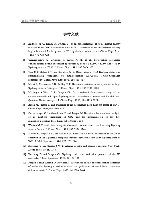
参考文献[1]Elidrissi M C, Roney A, Frigon C, et al. Measurements of total kinetic-energyreleased to the N=2 dissociation limit of H2 - evidence of the dissociation of very high vibrational Rydberg states of H2 by doubly-excited states. Chem. Phys. Lett.1994, 224:260-266[2]Yiannopoulou A, Urbanski K, Lyyra A M, et al. Perturbation facilitatedoptical-optical double resonance spectroscopy of the 2 3∑g+, 3 3∑g+, and 4 3∑g+ Rydberg states of 7Li2. J. Chem. Phys. 1995, 102:3024-3031[3]Tsai C C, Bahns J T, and Stwalley W C. Observation of Na2 Rydberg states andautoionization resonances by high-resolution All-Optical Triple-Resonance spectroscopy. Chem. Phys. Lett. 1995, 236:553-557[4]Merkt F, Mackenzie S R, Softley T P. Rotational autoionization dynamics in highRydberg states of nitrogen. J. Chem. Phys. 1995, 103:4509-4518[5]Mellinger A,Vidal C R, Jungen Ch. Laser reduced fluorescence study of thecarbon-monoxide nd triplet Rydberg series - experimental results and Multichannel Quantum-Defect Analysis. J. Chem. Phys. 1996, 104:8913-8921[6]Bixon M, Jortner J. The dynamics of predissociating high Rydberg states of NO. J.Chem. Phys. 1996,105:1363-1382[7]Cossartmagos C, Lefebvrebrion H, and Jungen M. Rotational band contour analysisof nf Rydberg complexes of CO2 and the determination of the first ionization-potential. Mol. Phys. 1995, 85:821-838[8]Warken M. Perturbation-theory for electronic excited-states - the low-lying Rydbergstates of water. J. Chem. Phys. 1995, 103:5554-5564[9]Matsui H, Mayer E E, and Grant E R. Bend-stretch Fermi resonance in NO2+ asobserved in the 2-photon absorption spectroscopy of the 3pσ 2∑u+ Rydberg state of NO2. J. Mol. Spectrosc. 1996, 175: 203-214[10]Herzberg G and Spinks J W T. Atomic spectra and atomic structure. New York:Dover publications, 1944.[11]Herzberg G and Jungen Ch. Rydberg series and ionization potential of the H2molecule. J. Mol. Spectrosc. 1972, 41:425-486[12]Jungen Chand Atabek O. Rovibronic interactions in the photoabsorption spectrumof molecular hydrogen and deuterium: an application of multichannel quantum defect methods. J. Chem. Phys. 1977, 66:5584-5609.97[13]Greene C and Jungen Ch. Molecular applications of quantum defect theory.Advances in Atomic and Molecular Physics. 1985, 21:51-121[14]Arif M, Jungen Ch, and Roche AL. The Rydberg spectrum of CaF and BaF:calculation by R-matrix and generalized quantum defect theory. J. Chem. Phys.1997, 106:4102-4118[15]Lewis B R, Banerjee S S, and Gibson S T. Asymmetric line-shapes in the indirectpredissociation of the F1∑g+ Rydberg state of O2. J. Chem. Phys. 1995, 102:6631-6640[16]Childs W J, Goodman L S, Nielsen U, et al. Electric-dipole moment of CaF(X2∑+)by molecular beam, laser-rf, double-resonance study of Stark splittings. J.Chem. Phys. 1984, 80:2283-2287[17]Selected Values of Electric Dipole Moments for Molecules in the Gas Phase. In:Weast R C, eds. CRC handbook of Chemistry and Physics, 55th edition. Clevland: CRC press, 1975: E-63[18]Rice S F, Martin H, and Field R W. The electronic structure of the calciummonohalides. A ligand field approach. J. Chem.Phys. 1985, 82:5023-5034[19]Berg J M, Murphy J E, Harris N A, et al. Observation and analysis ofcore-penetrating Rydberg states of calcium monofluoride. Phys. Rev. A, 1993, 48:3012-3029[20]Murphy J E, Berg J M, Merer A J, et al. Rydberg states and ionization potential ofcalcium monofluoride. Phys. Rev. Lett.1990, 65:1861-1864.[21]Harris N A and Jungen Ch. Rydberg states of calcium fluoride. Phys. Rev. Lett.1993, 70:2549-2552[22]Jabubek Z J and Field R W.Core-penetrating Rydberg series of BaF: s~p~d~fsupercomplexes. Phys. Rev. Lett. 1994, 72:2167-2170[23]马辉,李俭,刘耀明,等. 利用REMPI方法测量BaF高里德堡系列光谱. 化学物理学报. 1995,8:308-311[24]Carlson N W, Taylor A J, Jones K M, et al. Two-step polarization-labelingspectroscopy of excited states of Na2. Phys. Rev. A 1981, 24:822-834[25]Taylor A J, Jones K M and Schalow A L. Scanning pulsed-polarization spectrometerapplied to Na2. J. Opt. Soc. Am. 1983,73:994-998[26]Taylor A J, Jones K M and Schawlow A L. A study of the excited 1∑g+ states inNa2. Opt. Commun. 1981, 39:47-50[27]Shimizu K and Shimizu F. Laser induced fluorescence spectra of the a3∏u-X1∑g+band of Na2 by molecular beam. J. Chem. Phys. 1983, 78:1126-113198[28]Atkinson J B, Becker J, and Demtröder W. Experimental observation of the a3∏ustate of Na2. Chem. Phys. Lett. 1982, 87:92-97[29]Effantin C, d'Incan J, Ross A J, et al. Laser-induced fluorescence spectra of Na2 the(3s,3p) 1∑g+, (3s,3p) 1∏g and (3s,4s) 1∑g+ states. J.Phys. B 1984, 17:1515-1523 [30]Tsai C C, Whang T J, Bahns J T et al. The 31∑g+ “shelf” state of Na2.J. Chem.Phys. 1993, 99:8480-8488[31]Tsai C C, Bahns J T and Stwalley W C. Optical-optical double-resonancespectroscopy of the 51∑g+ shelf state of Na2 using an ultrasensitive ion detector. J.Chem. Phys. 1994, 100:768-774[32]Li Li and Field R W. Direct observation of high-lying 3∏g states of the Na2molecule by optical-optical double-resonance.J.Phys. Chem. 1983, 87: 3020-3022 [33]Whang T J, Tsai C C, Stwalley W C, et al. Spectroscopic study of the Na223∑g+state by cw perturbation-facilitated optical-optical double-resonance spectroscopy. J.Mol. Spectrosc. 1993, 160:411-421[34]Whang T J, Stwalley W C, Li Li, et al. Observatoins of the 3(3d)3∑g+ state of Na2.J. Mol. Spectrosc. 1992, 155:184-194[35]Whang T J, Stwalley W C, Li Li, et al. The Na2 43∑g+ state. J. Mol. Spectrosc.1993,157:544-547[36]Li Li and Field RW. CW optical-optical double resonance studies of the 23∏g,33∏g, 43∑g+ and 13∆g Rydberg states ofNa2. J. Mol. Spectrosc. 1986, 117:245 -282[37]Xie X, Field RW, Li Li, et al. Absolute vibrational numbering of the Na2 23∏gstate. J. Mol. Spectrosc. 1989, 134:119-128[38]Li Li, Lyyra AM, and Stwalley W C. Absolute vibrational numbering and molecularconstants of the Na2 13∆g state. J. Mol. Spectrosc. 1989, 134:113-118[39]Whang T J, Lyyra A M, Stwalley W C, et al. The Na2 23∆g state:CWperturbation-facilitated optical-optical double resonance spectroscopy. J. Mol.Spectrosc. 1991,149:505-511[40]Herzberg G. Molecular Spectra and Molecular StructureI.Spectra of DiatomicMolecules. New York: Van Nostrand Company, 1950.[41]Brown J M, Colbourn E A, Watson J K G, et al. An effective Hamiltonian fordiatomic molecules. J. Mol. Spectrosc. 1979,74:294-318[42]Kato H and Baba M. Dynamics of excited molecules: predissociation. Chem. Rev.1995, 95:2311-2349.99[43]Berg J M, Murphy J E, Harris N A, et al. Observation and analysis ofcore-penetrating Rydberg states of calcium monofluoride.Phys. Rev. A, 1993, 48:3012-3029.[44]Murphy J E, Berg J M, Merer A J, et al. Rydberg states and ionization potential ofcalcium monofluoride. Phys. Rev. Lett.1990, 65:1861-1864.[45]Harris N A and Jungen Ch. Rydberg states of calcium fluoride. Phys. Rev. Lett.1993, 70:2549-2552.[46]Jakubek Z J, Harris N A, Field R W, et al. Ionization-potentials ofCaF and BaF. J.Chem. Phys. 1994, 100:622-627.[47]Jabubek Z J and Field R W.Core-penetrating Rydberg series of BaF: s~p~d~fsupercomplexes. Phys. Rev. Lett. 1994, 72:2167-2170.[48]Jabubek Z J and Field R W. Core-penetrating Rydberg series of BaF: new electronicstates in the n*≈4 region. J.Mol.Spectrosc. 1996, 179: 99-124.[49]Harris NA and Field R W. The core-penetrating Rydberg series of the CaF molecule:at the borderline between valence and Rydberg states. J. Chem. Phys. 1993, 98:2642-2646.[50]Jakubek Z J and Field R W. Rydberg series of BaF: perturbation-facilitated studiesof core-nonpenetrating states. Philosophical Transactions Of The Royal Society Of London Series A-Mathematical Physical And Engineering Sciences. 1997, 355: 1507-1526[51]Arif M, Jungen Ch, and Roche AL. The Rydberg spectrum of CaF and BaF:calculation by R-matrix and generalized quantum defect theory. J. Chem. Phys.1997, 106:4102-4118[52]Torring T, Ernst W E, and Kandler J. Energies and electric diple moments of thelow lying electronic states of the alkaline earth monohalides from an electrostatic polarization model. J. Chem. Phys. 1989, 90:4927-4932[53]Guo B, Zhang K Q, and Bernath P F. High-resolution Fourier transform infraredemission spectra of barium monofluoride. J. Mol. Spectrosc. 1995, 170:59-74. [54]Ernst W E, Kindt S, Nair K P R, et al. Determination of the ground-state dipolemoment of CaCl from molecular-beam laser-microwave double-resonance measurements. Phys. Rev. A 1984, 29:1158-1163.[55]Ernst W E, Kändler J, and Törring T. Hyperfine structure and electric dipolemoment of BaF X2∑+. J. Chem. Phys. 1986, 84:4769-4773.[56]Childs W J, Goodman L S, Nielsen U, et al. Electric-dipole moment of CaF(X2∑+)by molecular beam, laser-rf, double-resonance study of Stark splittings. J.Chem. Phys. 1984, 80:2283-2287.100[57]Huber K P and G Herzberg. “Molecular Spectra and MolecularStructureIVConstantsof Diatomic Moleculars”, New York:Van Nostrand Reinhold, 1979[58]Harris N A. Rydberg spectroscopy of calcium monofluoride and calciummonochloride: [Ph.D. dissertation]. Department of Chemistry, MIT, 1995.[59]Domaille P J, Steimle T C, and Harris D O. The rotational spectrum of the X2∑+state of the Ca35Cl radical using laser microwave optical double resonance.J.Mol.Spectrosc. 1977, 66:503-505.[60]Berg L E, Klynning L, and Martin H. Observation of two photon absorption ingaseous CaCl. A study of the D2∑ and X2∑ states. Physica Scripta 1978, 18:61-64.[61]Berg L E, Klynning L, and Martin H. Laser spectroscopic investigation of CaCl. I.Rotational analysis of the A2∏-X2∑ transition. Physica Scripta 1980, 21:173-178.[62]Berg L E, Klynning L, and Martin ser spectroscopic investigations of CaCl. II.Rotational analysis of the B2∑+-X2∑+ transitions. Physica Scripta 1980, 22:216-220.[63]Klynning L, and Martin H. A study of the X2∑potential energy curves of thegaseous calcium chloride molecule. Physica Scripta 1980, 22:221-223.[64]Ernst W E, Schroder J O, Buck U, et al. Combined analysis of laser and microwavespectroscopy on CaCl: the A2∏- X2∑+ and B2∑+- X2∑+ systems. J.Mol.Spectrosc.1986, 117:342-354.[65]Gittins C M. Electronic structure and electronic-vibrational energy exchange inRydberg states of calcium monofluoride: [Ph.D. dissertation]. Department of Chemistry, MIT, 1995.[66]Smalley R E, Wharton L, and Levy D H. The fluorescence excitation spectrum ofrotationally cooled NO2. J. Chem. Phys. 1975, 63:4977-4989.[67]Dagdigian P J, Cruse H W, and Zare R N. Radiative lifetime of the alkaline earthmonohalides. J. Chem. Phys. 1974, 60:2330-2339.[68]Letokhov V S. Laser Photoionization Spectroscopy. Orlando: Academic Press,1987.[69]Berkowitz J. Photoabsorption, Photoionization, and Photoelectron Spectroscopy.New York: Academic Press, 1979.[70]Komatsu M, Ebata T, and Mikami N. Rotational analysis of n=4-7 Rydberg states ofCO observed by ion-dip spectroscopy.J. Chem. Phys. 1993, 99:9350-9365.[71]Komatsu M, Ebata T, Maeyama T, and Mikami N. Rotational structure anddissociation of the Rydberg states of CO by ion-dip spectroscopy. J. Chem. Phys.1995,103:2420-2435.101[72]Pribble R N and Zwier T S. Size-specific infrared-spectra of benzene-(H2O)nclusters (n=1-7) - evidence of noncyclic (H2O)n structures. Science 1994, 265:75-79.[73]Pribble R N, Garret A W, Haber K, et al. Resonant ion-dip Infrared spectroscopy ofbenzene-H2O and benzene-HOD. J. Chem. Phys. 1995,103: 531-544.[74]Earls L T. Intensities in 2∏-2∑transitions in diatomic molecules.Phys. Rev. 1935,48:423-424.[75]Rice S F, Martin H, and Field R W. The electronic structure of the calciummonohalides. A ligand field approach.J. Chem.Phys. 1985, 82:5023-5034[76]Lefebre-Brion H and Field R W. Perturbation in the Spectra of Diatomic Molecules.New York: Academic Press, 1986.[77]Kato H and Baba M. Dynamics of excited molecules: predissociation. ChemRev.1995, 95:2311-2349.[78]Herzberg G. Molecular Spectra and Molecular StructureI.Spectra of DiatomicMolecules. New York: Van Nostrand Company, 1950.[79]Tellinghuisen J. The Franck-Condon principle in bound-free transitions. In: LawleyK P, eds. Photodissociation and Photoionization. John Wiley&Sons Ltd.1985:299-369.[80]Barrow R F, Verges J, Effantin C, et al. Long-range potentials for the X1∑g+ and(1)1∏g states and the dissociation energy of Na2. Chem. Phys. Lett. 1984,104:179-183[81]Kusch P and Hessel M M. An analysis of the B1∏u-X1∑g+ band system of Na2. J.Chem. Phys. 1978, 68:2591-2606[82]Gerber G and Moller R. Optical-optical double resonance spectroscopy of highvibrational levels of the Na2 A1∑u+ state in a molecular beam. Chem. Phys. Lett.1985, 113:546-553[83]Carlson N W, Taylor A J, Jones K M, et al. Two-step polarization-labelingspectroscopy of excited states of Na2. Phys. Rev. A 1981, 24:822-834[84]Taylor A J, Jones K M and Schawlow A L. Scanning pulsed-polarizationspectrometer applied to Na2. J. Opt. Soc. Am. 1983,73:994-998[85]Taylor A J, Jones K M and Schawlow A L. A study of the excited 1∑g+ states inNa2. Opt. Commun. 1981, 39:47-50[86]Leutwyler S, Herrmann A, Woste L, et al. Isotope selective two-stepphotoionization study of K2 in a supersonic molecular beam. Chem. Phys. 1980, 48:253-267102[87]Leutwyler S, Heinis T, and Jungen M. Autoionizing Rydberg states in Na2. J. Chem.Phys. 1982, 76:4290-4292[88]Carlson N W, Taylor A J, Schawlow A L. Identification of Rydberg states in Na2 bytwo-step polarization labeling. Phys. Rev. Lett. 1980, 45:18-21[89]Carlson N W, Kowalski F V, Teets R E, et al. Identification of excited states in Na2by two-step polarization labeling. Opt. Commun. 1979, 29:302-306[90]Li Li and Field R W. Direct observation of high-lying 3∏g states of the Na2molecule by optical-optical double-resonance.J.Phys. Chem. 1983, 87: 3020-3022 [91]Kusch P and Hessel M M. Perturbations in the A1∑u+ state of Na2. J. Chem. Phys.1975, 63:4087-4088[92]Kaminsky M E, Hawkins R T, Kowalski F V, et al. Identification of absorption linesby modulated lower-level population: spectrum of Na2. Phys. RevLett. 1976, 36:671-673[93]Engelke F, Hage H, and Caldwell C D. Na2 b3∏u-X1∑g+ intercombinationbands:direct observation through high resolution laser fluorescence spectroscopy ina supersonic nozzle beam. Chem. Phys. 1982, 64:221-229[94]Atkinson J B, Becker J, and DemtrÖder W. Experimental observation of the a3∏ustate of Na2. Chem. Phys. Lett. 1982, 87:92-97[95]"Molecular Dynamics and Spectroscopy by Stimulated Emission Pumping", Chapter7, edited by Dai H L and Field R W, World Scientific, 1993.[96]Kovacs I. Rotational Structure in the Spectra of Diatomic Molecules. AcademicaElsevier, 1969.[97]Liu Y M, Li J, Xue M, et al. The Doubly Excited 1 3∑g- state of Na2: observationand calculation. J. Chem. Phys. 1995, 103:7213-7217[98]Shimizu K and Shimizu F. Laser induced fluorescence spectra of the a3∏u-X1∑g+band of Na2 by molecular beam. J. Chem. Phys. 1983,78, 1126-1131[99]Kato H, Otani M, and Baba M. Perturbations of the A1∑u+ and b3∏u states of Na2andthe effects on the transition intensity and the line splitting. J. Chem. Phys. 1988, 89:653-659[100]Li M, Wang C, Wang Y, et al. Polarization spectroscopy of Na2 A1∑u+- b3∏u←X1∑g+ intercombination bands.J. Mol. Spectrosc. 1987, 123:161 -166 [101]Whang TJ, Stwalley WC, Li Li, et al. Perturbation-Facilitated all-optical triple resonance spectroscopy of the Na2 b3∏u state. J. Chem. Phys. 1992, 97:7211-7219 [102]Bordas C, Labastie P, Chevaleyre J, et al. MQDT analysis of rovibrational interactions and autoionization in Na2 Rydberg states. Chem. Phys. 1989, 129:21-39103[103]Tsai C C, Bahns J T, and Stwalley W C. Observation of Na2 Rydberg states and autoionization resonances by high resolution all-optical triple resonance spectroscopy. Chem. Phys. Lett. 1995, 236:553-557[104]Henriet A and Masnou-Seeuws F. The spuvinage method for alkali dimers: III.potential energy curves for the excited states of Na2 up to the (3p+3p) dissociation limit. J.Phys. B 1987, 20:671-691.[105]Rohmer M M, Ernenwein R, Ulmschneider M, et al. Ab initio SCF calculations on [V10O28]6-: a benchmark for the classical calculation and processing of molecular intergrals on large Gaussian basis sets.Int.J.Quantum Chem. 1991, 40:723-744, and references therein.[106]Anderson K, Fulscher M P, Lindh R, et al. METECC-94, edited by EClementi (STEF, Cagliari, 1993).Jeung G H and Ross A J. Electronic structure of the lowest 1,3∑g+, 1,3∑u+, 1,3∏g, 1,3∏u, 1,3∆g and 1,3∆u states of K2 from valence CI calculations.J.Phys. B 1988, 21:1473-1487[107]Liu Y M, Li J, Gao H, et al. Predissociation of the Na2 33∏g State. J. Chem. Phys., 1998, 108:2269-2276[108]Li Li and Field RW. CW optical-optical double resonance studies of the 23∏g, 33∏g, 43∑g+ and 13∆g Rydberg states of Na2. J. Mol. Spectrosc. 1986, 117:245 -282[109]Whang T J, Lyyra A M, Stwalley W C, et al. The Na2 23∆g state: CW perturbation-facilitated optical-optical double resonance spectroscopy. J. Mol.Spectrosc. 1991,149:505-511[110]Li Li, Zhu Q, and Field RW. The hyperfine structure of the Na2 43∑g+ state.Mol.Phys. 1989, 66:685-694[111]Whang T J, Stwalley WC, Li Li, et al. The Na2 43∑g+ state. J. Mol. Spectrosc.1993,157:544-547[112]Li Li and Li M. Deperturbation of the Na2 43∑g+ v=4 ~ 33∏g v=6 and 43∑g+ v=14 ~ 23∏g v=68 interactions. J. Mol. Spectrosc. 1995,173:25-36[113]Xie X, Field RW, Li Li, et al. Absolute vibrational numbering of the Na2 23∏g state. J. Mol. Spectrosc. 1989, 134:119-128[114]Magnier S, Millie Ph, Dulieu O, et al. Potential curves for the ground and excited states of the Na2 molecule up to the (3s+5p) dissociation limit: results of two different effective potential calculations. J. Chem. Phys. 1994, 98:7113-7125 [115]Ji B, Tsai C C, Li Li, et al. Determination of the long-range potential and dissociation energy of the 13∆g state of Na2. J. Chem. Phys. 1995, 103: 7240-7254104[116]Li J, Liu Y M, Gao H, et al. Pulsed Perturbation Facilitated OODR Spectroscopy of the 4,7,10 3∆g Rydberg States of Na2. J. Mol. Spectrosc. 1996, 175:13-20[117]Li Li, Lyyra AM, and Stwalley W C, et al. The Na2 41∑g+~23∏g~13∆g triple perturbation: deperturbation of the (v∑, v∏, v∆)=(6,2,7) and (7,3,8) interactions.J. Mol.Spectrosc. 1991, 147:215-228[118]Fano U. Effects of configuration interaction on intensities and phase shifts. Phys. Rev.1961, 124, 1866-1878.[119]Martin S, Chevaleyre J, Bordas M C, et al. Autoionizing Rydberg states of the Na2 molecule. Chem. Phys. Lett. 1982,87:235-239.[120]Martin S, Chevaleyre J, Bordas M C, et al. Highly excited Rydberg states of Na2: decoupling between electronic and nuclear motion. J. Chem. Phys. 1983,79:4132-4141.105。

关于科学的英语演讲稿关于科学的英语演讲稿the presence of students, ladies and teachers, everyone! i was prepared intervals of cloud today, in honor here entitled “technology and future” speech, i am very proud of both, but some unease. in recent years, we have seen our great motherland, the cause of the rapid development of technology, which allow me to a chinese i feel very proud. remember that long ago, cell phone use almost the only one, which is called, but a few years ago, cell phones has undergone great changes, not only look more beautiful, but also use more, you can use the phones to take pictures, meetings, internet, text messages, etc. a series of things that i their life more convenient, so i am more aware of the strength of the technology, but i am just a fledgling s students, “technology” as the word also aware of the limited, i am unable to use some very difficult theory to elaborate technology xuanji, no right to work on their elders i can promise of the technology blueprint. but i am willing to use a student’s perspective to the imagine technology and the future.from genetic engineering “is a live princes” dream, nano-technology “- not washing your clothing,” promises; fromartificial intelligence “will give you a cute robot dog” warm, transgenic technology “let people grow mouse ears” wonders. the new technology in the birth of a new technology that will let people wild with joy, because these new technologies is gradually improving our lives, let us learn more about ourselves. in the near term, china completed its first sars virus genome sequencing, sars is now the world’s largest recognized the dangers of the disease, but why not other countries completed first, and we just completed the countries? very si-mp-le, this illustrates that our country backward than others, worse than others, we look at the past, had just started a country’s reform and opening up to the current level of science and technology has lead a large country, our motherland experienced a number of ups and downs, how many difficulties and bumpy however, we still back all of the motherland, the motherland because we firmly believe that - not only technological change destiny, can change the future.for our generation, the general feeling of the community is a strong sense of competition, learning a foot down. science knowledge is the focus of our attention, albert einstein, and stephen hawking, bill gates is the star we have in mind, computer science, physics and chemistry of modern dynamic is constantly affect us. we have to understand theimportance of technology, know that the technology universal.although technology to create a new life prospects soliciting thoughts, inspiring. however, the final analysis is that we rely on our common efforts to realize. , as the future construction of the backbone of our generation of young people shoulders the burden is not light, new opportunities are always accompanied risks and challenges, but we will not give up that easily, we use our youth to predecessors vowed: never live up to their predecessors of our hope.looking back at the history of civilization, anderson is the history of mankind against the darkness of ignorance, is the scientific lit a fire in the raging human soul of hope; technology support civilization, science and technology to create the future, but the future is in our hands. let us become knowledge explorers, let us unknown roaming on the road, let me use our creativity to the world we live a better place.参考翻译:在场的学生们,女士们,老师,大家好!我准备间隔云今天,为了纪念在这里题为“科技与未来”的讲话,我感到非常自豪的两个,但有些不安。
数字电路瞬态故障低能耗自修复方法司慧玲【摘要】当前大多数字电路瞬态故障修复方法需在人工处理下才可完成,修复效率低且能耗高.为此,提出一种新的数字电路瞬态故障低能耗自修复方法.设计了一种修复系统,其主要由自律控制模块与重配置执行模块构成,自律控制模块的核心是嵌入式NiosⅡ处理器.数字电路在出现瞬态故障的情况下,通过小波神经网络算法对数字电路瞬态故障进行诊断,判断电路是否正常运行.重配置执行模块包括逻辑计算节点LC与内部互联网络,主要作用是维持数字电路功能以及与其他模块之间施行信息传递.实验结果表明,所提方法能够有效诊断故障,故障修复成功率和平均适应度高,整体性能强.%At present,most of the digital circuit transient fault repair methods need to be completed by manual processing,the repair efficiency is low and the energy consumption is high.For this,a new kind of digital circuit fault transient low energy self repair method was put forward,design a repair system,which is mainly composed of self reconfiguration control module and execution module, self-discipline of the core control module is embedded Nios processor,digital circuit in the presence of transient fault.The wavelet neural network algorithm the diagnosis of digital circuit transient fault judging circuit,whether the normal operation of.The reconfiguration execution mod-ule consists of a logical computing node LC and an internal interconnection network.The main function is to main-tain the function of the digital circuit and carry out the information transmission between the other modules.The ex-perimental results show that the proposed method can effectively diagnose the fault,the successrate and the average fitness of the fault repair are high,and the overall performance is strong.【期刊名称】《科学技术与工程》【年(卷),期】2017(017)030【总页数】6页(P257-262)【关键词】数字电路;瞬态故障;低能耗;自修复【作者】司慧玲【作者单位】郑州工业应用技术学院机电工程学院,郑州451100【正文语种】中文【中图分类】TP331.2;TM932目前数字电路已经在不同产品上被广泛使用,在使用的过程中数字电路往往会出现一些瞬态故障,导致产品不能正常工作[1,2]。
ARTICLEReceived1Apr2014|Accepted9Jan2015|Published24Feb2015Observation of long-lived interlayer excitonsin monolayer MoSe2–WSe2heterostructuresPasqual Rivera1,John R.Schaibley1,Aaron M.Jones1,Jason S.Ross2,Sanfeng Wu1,Grant Aivazian1,Philip Klement1,Kyle Seyler1,Genevieve Clark2,Nirmal J.Ghimire3,4,Jiaqiang Yan4,5,D.G.Mandrus3,4,5, Wang Yao6&Xiaodong Xu1,2Van der Waals bound heterostructures constructed with two-dimensional materials,such asgraphene,boron nitride and transition metal dichalcogenides,have sparked wide interest indevice physics and technologies at the two-dimensional limit.One highly coveted hetero-structure is that of differing monolayer transition metal dichalcogenides with type-II bandalignment,with bound electrons and holes localized in individual monolayers,that is,interlayer excitons.Here,we report the observation of interlayer excitons in monolayerMoSe2–WSe2heterostructures by photoluminescence and photoluminescence excitationspectroscopy.Wefind that their energy and luminescence intensity are highly tunable by anapplied vertical gate voltage.Moreover,we measure an interlayer exciton lifetime of B1.8ns,an order of magnitude longer than intralayer excitons in monolayers.Our work demonstratesoptical pumping of interlayer electric polarization,which may provoke further explorationof interlayer exciton condensation,as well as new applications in two-dimensional lasers,light-emitting diodes and photovoltaic devices.1Department of Physics,University of Washington,Seattle,Washington98195,USA.2Department of Materials Science and Engineering,University of Washington,Seattle,Washington98195,USA.3Department of Physics and Astronomy,University of T ennessee,Knoxville,T ennessee37996,USA.4Materials Science and T echnology Division,Oak Ridge National Laboratory,Oak Ridge,T ennessee37831,USA.5Department of Materials Science and Engineering,University of T ennessee,Knoxville,T ennessee37996,USA.6Department of Physics and Center of Theoretical and Computational Physics, University of Hong Kong,Hong Kong,China.Correspondence and requests for materials should be addressed to P.R.(email:pasqual@)or to X.X. (email:xuxd@).T he recently developed ability to vertically assemble different two-dimensional(2D)materials heralds a newrealm of device physics based on van der Waals heterostructures(HSs)1.The most successful example to date is the vertical integration of graphene on boron nitride.Such novel HSs not only markedly enhance graphene’s electronic properties2, but also give rise to superlattice structures demonstrating exotic physical phenomena3–5.A fascinating counterpart to gapless graphene is a class of monolayer direct bandgap semiconductors, namely transition metal dichalcogenides(TMDs)6–8.Due to the large binding energy in these2D semiconductors,excitons dominate the optical response,exhibiting strong light–matter interactions that are electrically tunable9,10.The discovery of excitonic valley physics11–15and strongly coupled spin and pseudospin physics16,17in2D TMDs opens up new possibilities for device concepts not possible in other material systems. Monolayer TMDs have the chemical formula MX2where the M is tungsten(W)or molybdenum(Mo),and the X is sulfur(S) or selenium(Se).Although these TMDs share the same crystalline structure,their physical properties,such as bandgap,exciton resonance and spin–orbit coupling strength,can vary signifi-cantly.Therefore,an intriguing possibility is to stack different TMD monolayers on top of one another to form2D HSs.First-principle calculations show that heterojunctions formed between monolayer tungsten and molybdenum dichalcogenides have type-II band alignment18–20.Recently,this has been confirmed by X-ray photoelectron spectroscopy and scanning tunnelling spectroscopy21.Since the Coulomb binding energy in2D TMDs is much stronger than in conventional semiconductors, it is possible to realize interlayer excitonic states in van der Waals bound heterobilayers,that is,bound electrons and holes that are localized in different layers.Such interlayer excitons have been intensely pursued in bilayer graphene for possible exciton condensation22,but direct optical observation demonstrating the existence of such excitons is challenging owing to the lack of a sizable bandgap in graphene.Monolayer TMDs with bandgaps in the visible range provide the opportunity to optically pump interlayer excitons,which can be directly observed through photoluminescence(PL)measurements.In this report,we present direct observation of interlayer excitons in vertically stacked monolayer MoSe2–WSe2HSs.We show that interlayer exciton PL is enhanced under optical excitation resonant with the intralayer excitons in isolated monolayers,consistent with the interlayer charge transfer resulting from the underlying type-II band structure.We demonstrate the tuning of the interlayer exciton energy by applying a vertical gate voltage,which is consistent with the permanent out-of-plane electric dipole nature of interlayer excitons.Moreover,wefind a blue shift in PL energy at increasing excitation power,a hallmark of repulsive dipole–dipole interac-tions between spatially indirect excitons.Finally,time-resolved PL measurements yield a lifetime of1.8ns,which is at least an order of magnitude longer than that of intralayer excitons.Our work shows that monolayer semiconducting HSs are a promising platform for exploring new optoelectronic phenomena.ResultsMoSe2–WSe2HS photoluminescence.HSs are prepared by standard polymethyl methacrylate(PMMA)transfer techniques using mechanically exfoliated monolayers of WSe2and MoSe2(see Methods).Since there is no effort made to match the crystal lattices of the two monolayers,the obtained HSs are considered incom-mensurate.An idealized depiction of the vertical MoSe2–WSe2HS is shown in Fig.1a.We have fabricated six devices that all show similar results as those reported below.The data presented here are from two independent MoSe2–WSe2HSs,labelled device1and device2.Figure1b shows an optical micrograph of device1,which has individual monolayers,as well as a large area of vertically stacked HS.This device architecture allows for the comparison of the excitonic spectrum of individual monolayers with that of the HS region,allowing for a controlled identification of spectral changes resulting from interlayer coupling.We characterize the MoSe2–WSe2monolayers and HS using PL measurements.Inspection of the PL from the HS at room temperature reveals three dominant spectral features(Fig.1c). The emission at1.65and1.57eV corresponds to the excitonic states from monolayer WSe2and MoSe2(refs10,15),respectively. PL from the HS region,outlined by the dashed white line in Fig.1a,reveals a distinct spectral feature at1.35eV(X I).Two-dimensional mapping of the spectrally integrated PL from X I shows that it is isolated entirely to the HS region(inset,Fig.1c), with highly uniform peak intensity and spectral position (Supplementary Materials1).Low-temperature characterization of the HS is performed with 1.88eV laser excitation at20K.PL from individual monolayer WSe2(top),MoSe2(bottom)and the HS area(middle)are shown with the same scale in Fig.1d.At low temperature,the intralayer neutral(X M o)and charged(X MÀ)excitons are resolved10,15,where M labels either W or parison of the three spectra shows that both intralayer X M o and X MÀexist in the HS with emission at the same energy as from isolated monolayers,demonstrating the preservation of intralayer excitons in the HS region.PL from X I becomes more pronounced and is comparable to the intralayer excitons at low temperature.We note that the X I energy position has variation across the pool of HS samples we have studied (Supplementary Fig.1),which we attribute to differences in the interlayer separation,possibly due to imperfect transfer and a different twisting angle between monolayers.We further perform PL excitation(PLE)spectroscopy to investigate the correlation between X I and intralayer excitons.A narrow bandwidth(o50kHz)frequency tunable laser is swept across the energy resonances of intralayer excitons(from1.6to 1.75eV)while monitoring X I PL response.Figure2a shows an intensity plot of X I emission as a function of photoexcitation energy from device2.We clearly observe the enhancement of X I emission when the excitation energy is resonant with intralayer exciton states(Fig.2b).Now we discuss the origin of X I.Since X I has never been observed in our exfoliated monolayer and bilayer samples,if its origin were related to defects,they must be introduced by the fabrication process.This would result in sample-dependent X I properties with non-uniform spatial dependence.However,our data show that key physical properties of X I,such as the resonance energy and intensity,are spatially uniform and isolated to the HS region(inset of Fig.1c and Supplementary Fig.2).In addition,X I has not been observed in WSe2–WSe2homo-structures constructed from exfoliated or physical vapor deposi-tion(PVD)grown monolayers(Supplementary Fig.3).All these facts suggest that X I is not a defect-related exciton.Instead,the experimental results support the observation of an interlayer exciton.Due to the type-II band alignment of the MoSe2–WSe2HS18–20,as shown in Fig.2c,photoexcited electrons and holes will relax(dashed lines)to the conduction band edge of MoSe2and the valence band edge of WSe2,respectively.The Coulomb attraction between electrons in the MoSe2and holes in the WSe2gives rise to an interlayer exciton,X I,analogous to spatially indirect excitons in coupled quantum wells.The interlayer coupling yields the lowest energy bright exciton in the HS,which is consistent with the temperature dependence of X I PL,that is,it increases as temperature decreases (Supplementary Fig.4).From the intralayer and interlayer exciton spectral positions,we can infer the band offsets between the WSe 2and MoSe 2monolayers (Fig.2c).The energy difference between X W and X I at room temperature is 310meV.Considering the smaller binding energy of interlayer than intralayer excitons,this sets a lower bound on the conduction band offset.The energy difference between X M and X I then provides a lower bound on the valence band offset of 230meV.This value is consistent with the valence band offset of 228meV found in MoS 2–WSe 2HSs by micro X-ray photoelectron spectroscopy and scanning tunnelling spectro-scopy measurements 21.This experimental evidence strongly corroborates X I as an interlayer exciton.The observation of bright interlayer excitons in monolayer semiconducting HSs is of central importance,and the remainder of this paper will focus on their physical properties resulting from their spatially indirect nature and the underlying type-II band alignment.WSe 2HSMoSe 2W M SeIn te n s i t y (a .u .)1.31.51.7Energy (eV)MoSe 2HeterostructureWSe 2W0WX X X X −0MoMo−e hehe h1.3 1.41.51.6 1.7I n t e n s i t y (a .u .)Energy (eV)5μm 0123×104Y (μm )246X (μm)0246Figure 1|Intralayer and interlayer excitons of a monolayer MoSe 2–WSe 2vertical heterostructure.(a )Cartoon depiction of a MoSe 2–WSe 2heterostructure (HS).(b )Microscope image of a MoSe 2–WSe 2HS (device 1)with a white dashed line outlining the HS region.(c )Room-temperature photoluminescence of the heterostructure under 20m W laser excitation at 2.33eV.Inset:spatial map of integrated PL intensity from the low-energy peak (1.273–1.400eV),which is only appreciable in the heterostructure area,outlined by the dashed black line.(d )Photoluminescence of individual monolayers and the HS at 20K under 20m W excitation at 1.88eV (plotted on the samescale).Energy (eV)WSe MoSe PL energy (eV)E x c i t a t i o n e n e r g y (e V )1.28 1.3 1.32 1.34 1.36 1.381.61.651.71.754,0006,0008,00010,000IntensityFigure 2|Photoluminescence excitation spectroscopy of the interlayer exciton at 20K.(a )PLE intensity plot of the heterostructure region with an excitation power of 30m W and 5s charge-coupled device CCD integration time.(b )Spectrally integrated PLE response (red dots)overlaid on PL (black line)with 100m W excitation at 1.88eV.(c )Type-II semiconductor band alignment diagram for the 2D MoSe 2–WSe 2heterojunction.interlayer exciton .Applying vertical energy of Figure 3a contact stacked insu-Electrostatic contact shows the 100to about analogue of reversed,varied expected for from reduces device 2,conduction 3b,c.of the in the on top band-offset at X I PL energy of basis of would should have X I PL This effect,intensity.further Power dependence and lifetime of interlayer exciton PL .The interlayer exciton PLE spectrum as a function of laser power with excitation energy in resonance with X W o reveals several properties of the X I .Inspection of the normalized PLE intensity (Fig.4a)shows the evolution of a doublet in the interlayer excitonspectrum,highlighted by the red and Both peaks of the doublet display a consistent increased laser intensity,shown by the dashed which are included as a guide to the eye.intensity of X I also exhibits a strong saturation laser power,as shown in Fig.4b (absolute Supplementary Fig.6).The sublinear power excitation powers above 0.5m W is distinctly the intralayer excitons in isolated monolayers,saturation power threshold of about Fig.7).The low power saturation of X I PL lifetime than that of intralayer excitons.the intralayer exciton is substantially reduced interlayer charge hopping 23,which is quenching of intralayer exciton PL (Fig.Fig.8).Moreover,the lifetime of the interlayer because it is the lowest energy configuration indirect nature leads to a reduced optical long lifetime is confirmed by time-resolved Fig.4c.A fit to a single exponential decay exciton lifetime of 1.8±0.3ns.This timescale the intralayer exciton lifetime,which is ps 24–27.By modelling the saturation behaviour three-level diagram,the calculated saturation interlayer exciton is about 180times (Supplementary Fig.7;Supplementary with our observation of low saturation intensity DiscussionWe attribute the observed doublet feature splitting of the monolayer MoSe 2conduction assignment is mainly based on the fact difference between the doublet is B 25with MoSe 2conduction band splitting predicted calculations 28.This explanation is also supported by the evolution of the relative strength of the two peaks with increasing excitation power,as shown in Fig.4a (similar results in device 1with 1.88eV excitation shown in Supplementary Fig.9).At low power,the lowest energy configuration of interlayer excitons,with the electron in the lower spin-split band of MoSe 2,is populated first.Due to phase space filling effects,the interlayer excitonSiO 2n + Si2MoSe 2e –h +e –h +P Ee –h +V g < 0WSe 2MoSe 2WSe 2MoSe 2h ωV g = 0Photon energy (eV)1.321.361.41.444080e –h +h +PL intensity (a.u.) -hω’-the interlayer exciton and band alignment.(a )Device 2geometry.The interlayer exciton has a out-of-plane electric polarization.(b )Electrostatic control of the band alignment and the interlayer exciton photoluminescence as a function of applied gate voltage under 70m W excitation at 1.744eV,1s integrationconfiguration with the electron in the higher energy spin-split band starts to be filled at higher laser power.Consequently,the higher energy peak of the doublet becomes more prominent at higher excitation powers.The observed blue shift of X I as the excitation power increases,indicated by the dashed arrows in Fig.4a,is a signature of the repulsive interaction between the dipole-aligned interlayer excitons (cf.Fig.3a).This is a hallmark of spatially indirect excitons in gallium arsenide (GaAs)coupled quantum wells,which have been intensely studied for exciton Bose-Einstein condensation (BEC)phenomena 29.The observation of spatially indirect interlayer excitons in a type-II semiconducting 2D HS provides an intriguing platform to explore exciton BEC,where the observed extended lifetimes and repulsive interactions are two key ingredients towards the realization of this exotic state of matter.Moreover,the extraordinarily high binding energy for excitons in this truly 2D system may provide for degenerate exciton gases at elevated temperatures compared with other material systems 30.The long-lived interlayer exciton may also lead to new optoelectronic applications,such as photovoltaics 31–34and 2D HS nanolasers.MethodsDevice fabrication .Monolayers of MoSe 2are mechanically exfoliated onto 300nm SiO 2on heavily doped Si wafers and monolayers of WSe 2onto a layer of PMMA atop polyvinyl alcohol on Si.Both monolayers are identified with an opticalmicroscope and confirmed by their PL spectra.Polyvinyl alcohol is dissolved in H 2O and the PMMA layer is then placed on a transfer loop or thin layer of poly-dimethylsiloxane (PDMS).The top monolayer is then placed in contact with the bottom monolayer with the aid of an optical microscope and micromanipulators.The substrate is then heated to cause the PMMA layer to release from the transfer media.The PMMA is subsequently dissolved in acetone for B 30min and then rinsed with isopropyl alcohol.Low-temperature PL measurements .Low-temperature measurements are con-ducted in a temperature-controlled Janis cold finger cryostat (sample in vacuum)with a diffraction-limited excitation beam diameter of B 1m m.PL is spectrally filtered through a 0.5-m monochromator (Andor–Shamrock)and detected on a charge-coupled device (Andor—Newton).Spatial PL mapping is performed using a Mad City Labs Nano-T555nanopositioning system.For PLE measurements,a continuous wave Ti:sapphire laser (MSquared—SolsTiS)is used for excitation and filtered from the PL signal using an 815-nm-long pass optical filter (Semrock).Electrostatic doping is accomplished with an indium drain contact deposited onto the monolayer WSe 2region of device 2and using the heavily doped Si as a tunable backgate.Time-resolved PL measurements .For interlayer lifetime measurements,we excite the sample with a o 200-fs pulsed Ti:sapphire laser (Coherent—MIRA).Interlayer PL is spectrally filtered through a 0.5-m monochromator (Princeton—Acton 2500),and detected with a fast time-correlated single-photon counting system composed of a fast (o 30ps full width at half maximum)single-photon avalanche detector (Micro Photon Devices—PDM series)and a picosecond event timer (PicoQuant—PicoHarp 300).References1.Geim,A.K.&Grigorieva,I.V.Van der Waals heterostructures.Nature 499,419–425(2013).2.Dean,C.R.et al.Boron nitride substrates for high-quality graphene electronics.Nat.Nanotechnol.5,722–726(2010).3.Hunt,B.et al.Massive Dirac fermions and Hofstadter butterfly in a van derWaals heterostructure.Science 340,1427–1430(2013).4.Dean,C.R.et al.Hofstadter’s butterfly and the fractal quantum Hall effect inmoire superlattices.Nature 497,598–602(2013).5.Ponomarenko,L.A.et al.Cloning of Dirac fermions in graphene superlattices.Nature 497,594–597(2013).6.Novoselov,K.S.et al.Two-dimensional atomic crystals.Proc.Natl Acad.SciUSA 102,10451–10453(2005).7.Mak,K.F.,Lee,C.,Hone,J.,Shan,J.&Heinz,T.F.Atomically thin MoS 2:anew direct-gap semiconductor.Phys.Rev.Lett.105,136805(2010).8.Splendiani,A.et al.Emerging photoluminescence in monolayer MoS 2.NanoLett.10,1271–1275(2010).MoSe2WSe 2dPhoton energy (eV)Laser power (μW)Time (ns)I n t e n s i t y (a .u .)N o r m a l i z e d P L E i n t e n s i t y (c o u n t s (μW s )–1)Power (μW)I n t e g r a t e d P L E i n t e n s i t y (C o u n t s (μW s )–1)2060404Figure 4|Power-dependent photoluminescence of interlayer exciton and its lifetime at 20K.(a )Power dependence of the interlayer exciton for 1.722eV excitation with a bi-Lorentzian fit to the 5and 100m W plots,normalized for power and charge-coupled device (CCD)integration time.(b )Spectrally integrated intensity of the interlayer exciton emission as a function of excitation power shows the saturation effect.(c )Time-resolvedphotoluminescence of the interlayer exciton (1.35eV)shows a lifetime of about 1.8ns.The dashed curve is the instrument response to the excitation laser pulse.(d )Illustration of the heterojunction band diagram,including the spin levels of the MoSe 2conduction band.The X I doublet has energy splitting equal to (o 0I Ào I )E 25meV.9.Mak,K.F.et al.Tightly bound trions in monolayer MoS2.Nat.Mater.12,207–211(2013).10.Ross,J.S.et al.Electrical control of neutral and charged excitons in amonolayer mun.4,1474(2013).11.Xiao,D.,Liu,G.-B.,Feng,W.,Xu,X.&Yao,W.Coupled spin and valleyphysics in monolayers of MoS2and other group-VI dichalcogenides.Phys.Rev.Lett.108,196802(2012).12.Cao,T.et al.Valley-selective circular dichroism of monolayer molybdenummun.3,887(2012).13.Zeng,H.,Dai,J.,Yao,W.,Xiao,D.&Cui,X.Valley polarization inMoS2monolayers by optical pumping.Nat.Nanotechnol.7,490–493(2012).14.Mak,K.F.,He,K.,Shan,J.&Heinz,T.F.Control of valley polarization inmonolayer MoS2by optical helicity.Nat.Nanotechnol.7,494–498(2012). 15.Jones,A.M.et al.Optical generation of excitonic valley coherence inmonolayer WSe2.Nat.Nanotechnol.8,634–638(2013).16.Gong,Z.et al.Magnetoelectric effects and valley-controlled spin quantumgates in transition metal dichalcogenide mun.4,2053(2013).17.Jones,A.M.et al.Spin-layer locking effects in optical orientation of excitonspin in bilayer WSe2.Nat.Phys.10,130–134(2014).18.Kang,J.,Tongay,S.,Zhou,J.,Li,J.&Wu,J.Band offsets and heterostructuresof two-dimensional semiconductors.Appl.Phys.Lett.102,012111–012114 (2013).19.Kos´mider,K.&Ferna´ndez-Rossier,J.Electronic properties of the MoS2-WS2heterojunction.Phys.Rev.B87,075451(2013).20.Terrones,H.,Lopez-Urias,F.&Terrones,M.Novel hetero-layered materialswith tunable direct band gaps by sandwiching different metal disulfides and diselenides.Sci.Rep.3,1549(2013).21.Chiu,M.-H.et al.Determination of band alignment in transition metaldichalcogenide heterojunctions,Preprint at http://arXiv:1406.5137(2014). 22.Su,J.-J.&MacDonald,A.H.How to make a bilayer exciton condensateflow.Nat.Phys.4,799–802(2008).23.Hong,X.P.et al.Ultrafast charge transfer in atomically thin MoS2/WS2heterostructures.Nat.Nanotechnol.9,682–686(2014).24.Wang,G.et al.Valley dynamics probed through charged and neutral excitonemission in monolayer WSe2.Phys.Rev.B90,075413(2014).garde,D.et al.Carrier and polarization dynamics in monolayer MoS2.Phys.Rev.Lett.112,047401(2014).26.Mai,C.et al.Many-body effects in valleytronics:direct measurement of valleylifetimes in single-layer MoS2.Nano Lett.14,202–206(2013).27.Shi,H.et al.Exciton dynamics in suspended monolayer and few-layer MoS22Dcrystals.ACS Nano7,1072–1080(2012).28.Korma´nyos,A.,Zo´lyomi,V.,Drummond,N.D.&Burkard,G.Spin-orbitcoupling,quantum dots,and qubits in monolayer transition metaldichalcogenides.Phys.Rev.X4,011034(2014).29.Butov,L.V.,Lai,C.W.,Ivanov,A.L.,Gossard,A.C.&Chemla,D.S.TowardsBose-Einstein condensation of excitons in potential traps.Nature417,47–52 (2002).30.Fogler,M.M.,Butov,L.V.&Novoselov,K.S.High-temperature superfluiditywith indirect excitons in van der Waals mun.5,4555 (2014).31.Lee,C.H.et al.Atomically thin p-n junctions with van der Waalsheterointerfaces.Nat.Nanotechnol.9,676–681(2014).32.Furchi,M.M.,Pospischil,A.,Libisch,F.,Burgdorfer,J.&Mueller,T.Photovoltaic effect in an electrically tunable van der Waals heterojunction.Nano Lett.14,4785–4791(2014).33.Cheng,R.et al.Electroluminescence and photocurrent generation fromatomically sharp WSe2/MoS2heterojunction p-n diodes.Nano Lett.14,5590–5597(2014).34.Fang,H.et al.Strong interlayer coupling in van der Waals heterostructuresbuilt from single-layer chalcogenides.Proc.Natl A111,6198–6202 (2014).AcknowledgementsThis work is mainly supported by the US DoE,BES,Materials Sciences and Engineering Division(DE-SC0008145).N.J.G.,J.Y.and D.G.M.are supported by US DoE,BES, Materials Sciences and Engineering Division.W.Y.is supported by the Research Grant Council of Hong Kong(HKU17305914P,HKU9/CRF/13G),and the Croucher Foun-dation under the Croucher Innovation Award.X.X.thanks the support of the Cottrell Scholar Award.P.R.thanks the UW GO-MAP program for their support.A.M.J.is partially supported by the NSF(DGE-0718124).J.S.R.is partially supported by the NSF (DGE-1256082).S.W.and G.C.are partially supported by the State of Washington through the UW Clean Energy Institute.Device fabrication was performed at the Washington Nanofabrication Facility and NSF-funded Nanotech User Facility. Author contributionsX.X.and P.R.conceived the experiments.P.R.and P.K.fabricated the devices,assisted by J.S.R.P.R.performed the measurements,assisted by J.R.S.,A.M.J.,J.S.R.,S.W.and G.A. P.R.and X.X.performed data analysis,with input from W.Y.N.J.G.,J.Y.and D.G.M. synthesized and characterized the bulk WSe2crystals.X.X.,P.R.,J.R.S.and W.Y.wrote the paper.All authors discussed the results.Additional informationSupplementary Information accompanies this paper at / naturecommunicationsCompetingfinancial interests:The authors declare no competingfinancial interests. Reprints and permission information is available online at / reprintsandpermissions/How to cite this article:Rivera,P.et al.Observation of long-lived interlayer excitons in monolayer MoSe2–mun.6:6242doi:10.1038/ncomms7242(2015).。
a rX iv:c ond-ma t/99728v1[c ond-m at.s upr-con]2J ul1999Low-energy electronic structure in Y 1−x Ca x Ba 2Cu 3O 7−δ:comparison of time-resolved optical spectroscopy,NMR,neutron and tunneling data.J.Demsar,K.Zagar,V.V.Kabanov and D.Mihailovic ”J.Stefan Institute”,Jamova 39,1001Ljubljana,Slovenia February 1,2008Abstract Time-resolved optical measurements give information on the quasi-particle relaxation dynamics in YBCO,from which the evolution of the gap with doping and temperature can be systematically deduced.In this paper these optical charge-channel ”pseudogap”data are compared with the ”pseudogap”obtained from the NMR Knight shift K s ,spin polar-ized neutron scattering (SPNS)and single particle tunneling measure-ments.A simple energy level diagram is proposed to explain the different ”gap”magnitudes observed by different spectroscopies in YBa 2Cu 3O 7−δ,whereby the spin gap ∆s in NMR and SPNS corresponds to a triplet local pair state,while ∆p in the charge excitation spectrum corresponds to the pair dissociation energy.At optimum doping and in the overdoped state,an additional T -dependent gap becomes evident,which closes at T c ,sug-gesting a cross-over to a more conventional BCS-like superconductivity scenario.1Introduction Spectroscopic studies of cuprates over the years have shown that at low ener-gies these materials exhibit quite a complex spectral structure,which changes with temperature and doping in a complicated way.Often there appears to be reasonable agreement regarding some of the main features between various experimental techniques.For example,optical femtosecond quasiparticle relax-ation measurements and single-particle (Giever)tunneling show a similar size pseudogap in the spectrum over a large portion of the phase diagram,and the latter is remarkably similar to the spectral features measured by angle-resolved photoemission.However,the pseudogap ∆s as observed by spectroscopies like1NMR and spin-polarized neutron scattering appears to be smaller than the opti-cal and tunneling pseudogap∆p by approximately a factor of2,for which there is as yet no accepted theoretical explanation.Thus in spite of the availability of spectral data over a large range of doping in many materials,the interpretata-tion of the low-energy excitation spectrum is still highly controversial.In this paper we summarize some of the results of time-resolved quasiparticle recombi-nation spectroscopy as a function of doping and temperature in YBa2Cu3O7−δ, which appear to give qualitative new insight into the origin of the low-energy spectral features of this material and its phase diagram.We compare the doping-evolution of the pseudogap∆p obtained from time-resolved spectroscopy with a quantitative analysis of the”spin-gap”from the NMR knight shift K s in the underdoped state using the same type of T-independent gap as deduced from the quasiparticle relaxation data.Wefind that the time-resolved QP relax-ation data are quite consistent with Giever tunneling and ARPES data and suggest that all the observations together can be explained by the existence of a pair-breaking pseudogap∆p and a triplet-state local pair excitation∆s at E≈∆p/2.2Time-resolved spectroscopy resultsThe time-resolved optical spectroscopy applied to superconductors and other materials with a gap has been given in detail elsewhere[1,2],so here we shall discuss only the results.The equations describing the temperature dependence of photoexcited QP density and their lifetime as a function of temperature are given by Kabanov et al[1].Using these equations,the properties of the gap can be investigated as a function of doping and temperature.Systematic experi-ments on YBaCuO as a function of O concentration over a wide range ofδhave shown very clear and systematic behavior of the QP dynamics[1].Particularly important is that the results are quite insensitive to surface quality and have been repeated after a period of a year with the same results.Single crystals were also studied and no significant differences were found in comparison with the thinfilm data.These measurements have recently been extended to the over-doped state using calcium-doped(Y,Ca)Ba2Cu3O7−δcrystals by Demsar et al [2],giving data on the whole phase diagram from insulating and underdoped to overdoped YBCO.A typical time-resolved signal in the optimally doped phase is shown in Figure1.Above T c,one exponential short-lived decay is observed whose amplitude is decreasing as T is increased(Figure2),while below T c, two exponentials are clearly seen,one of which has a longer lifetime which is temperature-dependent and diverges as T→T c.Such behaviour is typical also for overdoped samples,but not for underdoped samples,where only a single exponential decay is observed,with a T-indendent time constantτp∼0.4ps showing no anomaly at T c.From these experiments we can deduce that in underdoped state the evolution of the QP dynamics with temperature and dop-2ing is dominated by a temperature-independent pseudogap∆p.Near optimum doping an additional BCS-like temperature-dependent gap∆BCS appears be-low T c,which is present also in all the overdoped samples[2]and gives rise to the additional temperature-dependent relaxation process below T c.The fact theτdiverges near T c unambiguously signifies that∆BCS→0at T c.Thus close to optimum doping and in the overdoped state two gaps appear to be present simultaneously,a feature consistent with the spatially inhomoge-neous ground state[3]in which the pair-breaking excitation is represented by ∆p,while the∆BCS is a gap associated with the collective behaviour of high-carrier density stripes or clusters which start to form near optimum doping.The values of the gaps∆p and∆BCS as a function of doping obtained byfitting the temperature dependence of the photoinduced signal amplitude as shown in Fig. 2with the model calculation of Kabanov et al[1]are plotted in Figure4.3Comparison with other spectroscopiesFrom the time-resolved data on the underdoped YBCO we have deduced that the low-energy spectrum can be described by a single temperature-independent gap∆p.Starting from this observation we decided to analyse the temperature dependence of the NMR Knight shift K s available from the literature using the same T-indepedent∆p.The aim is a)to see if the simple model can describe the T-dependence of K s and b)to see if the values of the pseudogap obtained for the NMR K s agree with the optical values.The NMR knight shift for such a case can be written as[4]K s=K0+AT−βexp[−∆s/k B T],where K0is the value of K s at zero temperature,βis an exponent which depends on the shape of the singularity of the DOS at the gap and A is a constant depending on the NMR nucleus.The results offits to published data in YBCO123and124on89Y[5],63Cu [6]and17O[7]are shown in Figure3usingβ=1/2.In spite of its simplicity,the model appears to describe the data very well.The gap values∆s withβ=1/2 obtained for YBa2Cu3O7−δare shown in Figure4.∆s appears consistently lower than the∆p by approximately a factor of2.Apart from NMR K s,spin-polarized neutron scattering(SPNS)also shows a spin-excitation peak at34meV(∼390K)in underdoped YBa2Cu3O6.6,which is smaller than∆p by approximately a factor of2.However,the anomalies in the phonons signifying the presence of charge excitations occur near70meV (∼810K),also approximately twice the spin excitation energy and very close to the∆p in Fig.4.(see Mook et al,this volume).To explain the two different gaps∆p and∆s,we propose a rather straightfor-ward electronic structure in YBCO.A schematic diagram is shown in the insert to Fig. 4.The ground state is composed of local S=0singlet Cooper pairs. Since∆p is a QP charge excitation it is clearly associated with pair breaking. However,if J<∆p,the triplet local pair state also exists and lies within the3gap.It should be visible by spin-flip spectroscopies like NMR and SPNS,but not by optical spectroscopy or SP tunneling which are charge excitations.We therefore propose that the∆s observed by NMR and SPNS is the S=1local pair triplet excited state.From the experimental data in Fig.4,both∆p and ∆s decrease with increasing doping,more or less as1/x,where x is the hole density.For low doping,atδ∼0.6,J≈800K,consistent with Raman and neutron measurements.We note that possibly the situation might be different in La2−x Sr x CuO4,where the optical gap and the NMR gap appear to have the same energy scale[8],suggesting that either J¿∆p in this material or that the triplet pair state is not a bound state in this material.In underdoped YBCO,at T c there is no anomaly in either the QP relaxation[1] or the NMR K s[5,6].Similarly the SPNS intensity at34meV shows no anomaly at T c itself,but only a gradual drop with increasing T.From this we can de-duce that there is no change in the DOS at T c in the underdoped state,and that all changes of the DOS are gradual with T.This is equivalent to there being no condensation energy associated with the superconducting transition itself which is consistent with the Bose condensation of local pairs scenario,where at T c macrosopic phase coherence is established with no change in pairing am-plitude.A3D superconducting state forms when phase coherence percolates through the entire sample resulting in a transition to a coherent macroscopic state at T c.In contrast,in optimally doped and overdoped YBCO as the carrier density increases,the pairs begin to overlap,collective effects become important and a transition to a more conventional BCS-like scenario takes place[1].QP relaxation,NMR K s,SPNS and tunneling data all show an abrupt anomaly at T c signifying that pairing and phase cohrence occur at the same(or nearly the same)temperature.The most important feature of the QP relaxation data not available from other spectroscopies is the simultaneous unambiguous observation of2gaps in optimally doped and overdoped samples,one T-independent∆p and the other T-dependent∆BCS,with a BCS-like T dependence.References[1]V.V.Kabanov,et al Phys.Rev.B59,1497(1999),J.Demsar et al,Europhys.Lett.45,381(1999)[2]J.Demsar,B.Podobnik,V.V.Kabanov,D.Mihailovic and T.Wolf,subm.toPhys.Rev.Lett(1998)[3]D.Mihailovic and K.A.M¨u ller,p243”High-T c Superconductivity1996:Tenyears after the Discovery”Ed.E.Kaldis,E.Liarokapis,K.A.Muller NATO Series E:Applied Sciences vol.343(Kluwer Academic Publishers1997)4[4]A.S.Alexandrov,V.V.Kabanov and N.F.Mott,Phys.Rev.Lett.77,4796(1996)[5]H.Alloul,T.Ohno,P.Mendels,Physica162-164,193(1989)[6]Curro et al,Phys.Rev.B56,877(1997)[7]Williams et al,Phys.Rev.Lett.78,721(1998)[8]K.A.M¨u ller,Guo-meng Zhao,K.Conder and H.Keller,J.Phys.:Condens.Matter10,L291(1998)5the two-.BCS6ofCa1]7ininet8The areThe。