索尼随声听WM-FX493电路原理图
- 格式:pdf
- 大小:2.04 MB
- 文档页数:18
常见传声器的结构及工作原理传声器又称话筒,它是将声音信号转换为电信号的电声器件。
传声器的种类很多,若按换能原理分有电容式、压电式、驻极体电容式、电动动圈式、带式电动式以及碳粒式等,现在应用最广的是电动动圈式和驻极体电容式两大类。
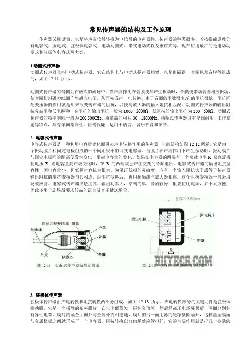
1.动圈式传声器动圈式传声器又叫电动式传声器,它在结构上与电动式扬声器相似,也是由磁铁、音圈以及音膜等组成的,如图12-11 所示。
动圈式传声器的音圈处在磁铁的磁场中,当声波作用在音膜使其产生振动时,音膜便带动音圈相应振动,使音圈切割磁力线而产生感应电压,从而完成声一电转换。
由于音圈的阻数很少.它的阻抗很低,阻抗匹配变压器的作用就是用来改变传声器的阻抗,以便与放大器的输入阻抗相匹配。
动圈式传声器的输出阻抗分高阻和低阻两种,高阻抗的输出阻抗一般为1000 - 2000Ω,低阻抗的输出阻抗为200 - 600Ω。
动圈式传声器的频率响应一般为200 5000Hz,质量高的可达30 - 18000Hz。
动圈式传声器具有坚固耐用、工作稳定等特点,具有单向指向性,价格低廉,适用于语言、音乐扩音和录音。
2. 电容式传声器电容式传声器是一种利用电容量变化而引起声电转换作用的传声器,它的结构如图12-12所示,它是由一个振动膜片和固定电极组成的一个间距很小的可变电容器。
当膜片在声波作用下产生振动时,振动膜片与固定电极间的距离便发生变化,引起电容量的变化。
如果在电容器的两端有一个负载电阻R 及直流极化电压E. 则电容量随声波变化时,在R 的两端就会产生交变的音频电压。
电容式传声器的输出阻抗呈容性,因电容量小,但低频时容抗会很大。
为保证低频的灵敏度,应有一个输入阻抗大于或等于传声器输出阻抗的阻抗变换器与其相连,经阻抗变换后,再用传输线与放大器相连。
这个阻抗变换器一般采用场效应管。
电容式传声器灵敏度高,输出功率大,结构简单,音质较好,但要使用电源,并不太方便,因此多用于剧场及要求较高的语言及音乐播送场合。
![MP3工作原理[图解]](https://uimg.taocdn.com/34e1ca4df7ec4afe04a1df22.webp)
MP3全称是MPEG Audio Layer 3,MPEG压缩格式是由运动图像专家组(Motion Picture Experts Group)制定的关于影像和声音的一组标准,其中MP3就是为了压缩声音信号而设计的是一种新的音频信号压缩格式标准。
CD唱片采样率频率为44.1MHz, 16Bits, 数据量为1.4Mbps,而相应的MP3数据量仅为112kbps或128kbps,是原始数据量的1/12。
也就是说传统的一张CD现在可以存放10倍甚至更多容量的音乐,但是在人耳听起来, 感受到的音乐效果却没有什么不同。
MP3随身听的工作原理,其实很简单,反正就是有一块不知什么型号的控制芯片,控制解码芯片和LCD液晶屏,由解码芯片把内置闪存或是外插闪存卡之中的MP3文件解码,然后经数模转换,最后从耳机输送到我们的耳朵中。
也就是说一共没几块芯片。
你如果拆一个MP3随身听看看,你会发现里面比较大的半导体芯片只有4、5片。
现在新一代的MP3随身听在技术上是非常先进的,最具代表性的是NOMAD II,基于美国CirrusLogic最新的EP7209 MCU(微程序控制器)芯片组,它的作用实际上就像电脑里的CPU,经过软件解码,可以支持多种网络音乐格式,包括MP3,以及日后的WMA格式。
而国内使用这种芯片制造的MP3随身听也即将问世。
起初,MP3文件只能由电脑来播放,而随着互联网的发展,文件小、音质可与CD媲美的MP3音乐越来越适合人们在Internet上传递,而广为流行。
再加上全世界范围内的MP3下载网站泛滥,使人们传统的听音乐习惯发生了改变。
MP3的逐渐流行,随时随地欣赏MP3音乐的需求越来越高,这就创造了MP3播放器的市场。
越来越多的各种类型的MP3随身听不断问世,MP3随身听已经成为续MD 之后新兴的随身娱乐设备的亮点。
目前,在全球市场上的MP3随身听有几十种之多,在中国销售的也有十种以上。
CVC的1系列和2系列,三星的YEPP系列,世韩的MPMAN系列都是其中的佼佼者。
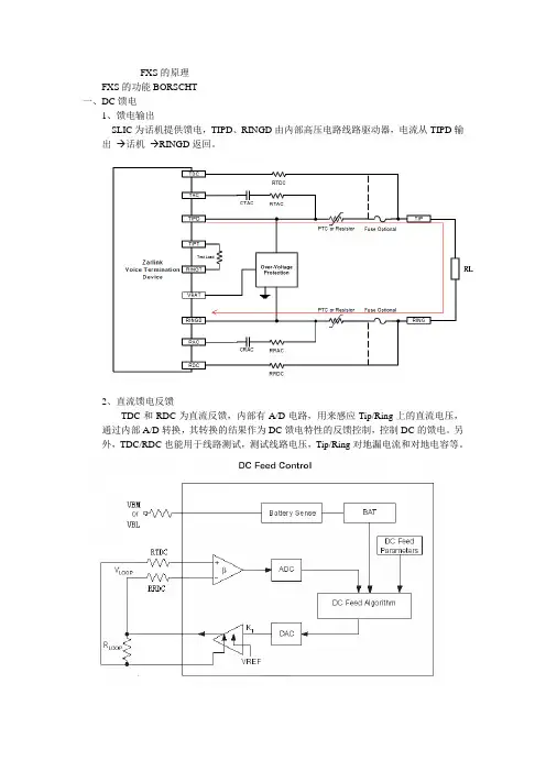
FXS的原理FXS的功能BORSCHT一、DC馈电1、馈电输出SLIC为话机提供馈电,TIPD、RINGD由内部高压电路线路驱动器,电流从TIPD输出→话机→RINGD返回。
2、直流馈电反馈TDC和RDC为直流反馈,内部有A/D电路,用来感应Tip/Ring上的直流电压,通过内部A/D转换,其转换的结果作为DC馈电特性的反馈控制,控制DC的馈电。
另外,TDC/RDC也能用于线路测试,测试线路电压,Tip/Ring对地漏电流和对地电容等。
3、馈电特性曲线馈电特性曲线分两段,恒流区和恒压区,在短距离摘机时,SLIC处于恒流区,在话机或长距离摘机,SLIC处于恒压区。
4、摘挂机检测SLIC摘挂机检测是检测环路电流,检测门限是可编程的,一般设置为10MA,当电流从0增大到10MA时,SLIC上报摘机信息,当电流从大降低到8MA时,SLIC上报挂机。
二、过压、有流保护当电话线出户时,可能会遭受到雷击、电力线碰接等,因此在SLIC的TIP/RING需要加过压和过流保护。
1、SLIC Tip/Ring能承受的最大电压2、PTCPTC是正温度特性的热敏电阻,温度升高电阻阻值变大,当电话线碰接到电力线时,因流过的电流大,使得PTC的电阻迅速变大,最终断开外线与SLIC的TIPD/RINGD 的连接3、过压保护器件SVG170D三、振铃1、铃流输出SLIC的振铃信号的幅度、频率是软件可编程的,最大幅度Vpk=|VBH|-4,振铃信号由A信号产生器产生低压的铃流信号,经SLIC高压驱动放大器放大输出,在TIP/RING差分输出。
在振铃期间,SLIC等效为内阻200欧姆的信号源。
2、振铃期间摘机检测(Ring Trip)振铃期间摘机检测是检测2个周期内的平均电流,当平均电流大于检测门限时,SLIC上报摘机,门限是可编程的四、语音信号以下是SLIC语音输入、输出的示意图,下行的语音信号(输出)是调制在馈电电流上,上行语音信号(输入)是电压信号。
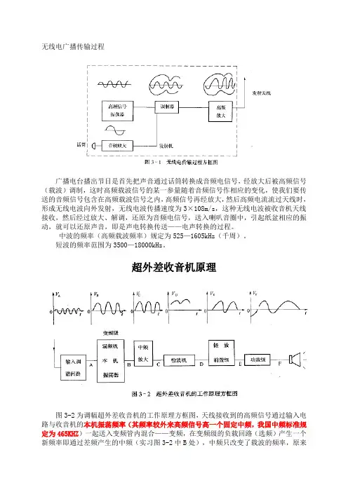
无线电广播传输过程广播电台播出节目是首先把声音通过话筒转换成音频电信号,经放大后被高频信号(载波)调制,这时高频载波信号的某一参量随着音频信号作相应的变化,使我们要传送的音频信号包含在高频载波信号之内,高频信号再经放大,然后高频电流流过天线时,形成无线电波向外发射,无线电波传播速度为3×10⁸m/s,这种无线电波被收音机天线接收,然后经过放大、解调,还原为音频电信号,送入喇叭音圈中,引起纸盆相应的振动,就可以还原声音,即是声电转换传送——电声转换的过程。
中波的频率(高频载波频率)规定为525—1605kHz(千周)。
短波的频率范围为3500—18000kHz。
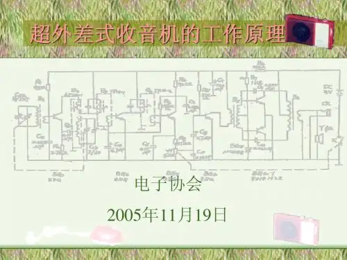
超外差收音机原理图3-2为调幅超外差收音机的工作原理方框图,天线接收到的高频信号通过输入电路与收音机的本机振荡频率(其频率较外来高频信号高一个固定中频,我国中频标准规定为465KHZ)一起送入变频管内混合——变频,在变频级的负载回路(选频)产生一个新频率即通过差频产生的中频(实习图3-2中B处),中频只改变了载波的频率,原来的音频包络线并没有改变,中频信号可以更好地得到放大,中频信号经检波并滤除高频信号(实习图3-2中D处)。
再经低放,功率放大后,推动扬声器发出声音。
本机工作原理简述。
电路图见实习图3-3所示C1、B1组成天线输入回路。
VT1、B2、B1、C组成变频级。
VT1为变频管。
初级线圈与C构成变频级负载。
C1、B2组成本机振荡电路,C6为振荡耦合电路,VT2、VT3组成中频放大电路,2AP9为检波电路,R9为音量电位器(带电源开关),C16为高频耦合电容。
VT4、VT5为前置低频放大级、VT6、VT7组成乙类推挽功率放大器。
R16、C21、C17为电源波波电路。
R1、R2、R3、R4、R5、R6、R7、R12、R10、R11、R13、R17、R18为各级的直流偏置电阻。
超外差收音机超外差收音机的安装:①整机电路分析,熟悉元件在印刷板上安装位置。
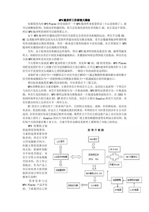
MP3随身听工作原理大揭秘如果您因为对MP3 Player好奇而拆开一个MP3随身听来看看的话(小心没保修了),就可以清晰地看到:里面没有机械结构,你只会发现里面有好多块贴片IC。
也正是这个原因,所以MP3随身听的体积可以做得那么小。
由于MP3随身听在播放过程中的信号流程完全没有涉及机械的运动,所以不会像CD、MD这类随身听那样会因为光头受到外界震动而发生跳音现象,更不会像磁带随身听那样要有传动机械而出现绞带现象。
所以一般来说只要你的储存卡没有问题,在正常情况下MP3随身听在播放时绝不会出现跳音等现象。
另外,由于机体没有机械式运作部件,所以MP3随身听的耗电量没有CD、磁带等随身听大,而相信以后其芯片的技术越来越成熟后,其播放时间将会得到很大的提高,所以在这方面MP3随身听还有比较大的潜力!今天想和大家谈谈MP3随身听的工作原理。
其实和MD机、CD机等类似,MP3 Player 同样也是把贮存卡上的数子信号送到解码芯片进行解码,只不过MP3随身听读取存贮卡上的信号并不是使用光头或磁头之类的机械部件。
一般的工作的流程是这样的:读取贮体上的信号-→到解码芯片对信号进行解码-→通过数模转换器将解出来的数字信号转换成模拟信号-→再把转换后的模拟音频放大-→低通滤波后到耳机输出口。
想比较直观地看看MP3的内部结构,可以参看以下三篇文章:MP3的整机设计方案有数种,主要有单芯片和双芯片之分。
这里给大家说明一下单芯片与双芯片是怎么回事:双芯片是控制部分为一片集成电路、MP3解码运算部分为一片集成电路;单芯片是控制部分、MP3解码运算部分都集成在一片集成电路里面的芯片。
在2002年初的时候单芯片的方案以ST、EP的芯片为代表,双芯片主要以Sunplus的芯片为代表。
双芯在推出时间上比单芯片早一两年左右。
ST的芯片主要应用于三星系列产品中,它的特点是稳定,成熟。
但价格较高、而且没有录音、复读的功能,在这点上不能满足我们的要求。

SERVICE MANUALLEVEL2DSC-P10/P12•For ADJUSTMENTS (SECTION 6), refer to SERVICE MANUAL, ADJ (987622751.pdf).•For INSTRUCTION MANUAL, refer to SERVICE MANUAL, LEVEL 1 (987622741.pdf).•This service manual contains information for Japanese model as well.•Reference No. search on printed wiring boards is available.•Note in Lens Frame Installation•HELP: Sheet attachment positions and procedures of processing the flexible boards/harnesses are shown.DIGITAL STILL CAMERAOn the JK-243, JK-244 and SY-83 boardsThis service manual procides the information that is premised the circuit board replacement service and not intended repair inside the JK-243, JK-244 and SY -83 boards.Therefore, schematic diagram, printed wiring board andelectrical parts list of the JK-243, JK-244 and SY -83 boards are not shown.The following pages are not shown.JK-243, JK-244 boardsSchematic diagram .........................Pages 4-35 to 4-36Printed wiring board ........................Pages 4-51 to 4-52Electrical parts list...........................Pages 5-6SY-83 boardSchematic diagram .........................Pages 4-9 to 4-28Printed wiring board ........................Pages 4-43 to 4-46Electrical parts list...........................Pages 5-9 to 5-13The above-described information is shown in service manual Level 3.Photo: DSC-P10US Model Canadian ModelDSC-P10AEP Model UK ModelDSC-P10/P12E ModelHong Kong Model Australian Model Chinese Model Korea Model T ourist Model Japanese ModelDSC-P10SPECIFICATIONSWhite balanceFlash, Automatic, Daylight, Cloudy,Fluorescent, IncandescentData format (DCF compliant)Still images: Exif Ver. 2.2 JPEGcompliant, GIF (for Clip Motion),DPOF compatibleAudio with still image:MPEG1 compliant (Monaural)Moving images:MPEG1 compliant (Monaural) Recording media“Memory Stick”Flash Recommended distance (ISO set to Auto):0.5 m to 3.5 m (193/4 inches to11feet 5 3/16 inches) (W)0.6 m to 2.5 m (235/8 inches to 8feet27/16 inches) (T)[Output connectors]A/V OUT (MONO) (Monaural)MinijackVideo: 1 Vp-p, 75 Ω, unbalanced,sync negativeAudio:327 mV (at a 47 kΩ load)Output impedance 2.2 kΩUSB jack mini-B[General]Used battery packNP-FC11Power requirements3.6VPower consumption (during shooting)1.6 WOperating temperature0°C to 40°C (32°F to 104°F)Storage temperature–20°C to +60°C (–4°F to +140°F)Dimensions108×51.5×35.1 mm(4 3/8×21/8×17/16 inches)(W/H/D, excluding maximumprotrusions)Mass Approx. 200 g (7 oz) (includingbattery pack NP-FC11, “MemoryStick” and wrist strap)Built-in microphoneElectret condenser microphoneBuilt-in speakerDynamic speakerExif Print CompatiblePRINT image matching II CompatibleStorage temperature–20°C to +60°C (–4°F to +140°F)DimensionsApprox. 48×29×81mm(1 15/16×1 3/16×3 1/4 inches)(W/H/D)Mass Approx. 130g (5oz)x NP-FC11 battery packUsed batteryLithium-ion batteryMaximum voltageDC 4.2VNominal voltageDC 3.6VCapacity 2.8Wh (780mAh)Accessories•NP-FC11 battery pack (DSC-P12: 2, DSC-P10: 1)•AC-LS5AC Adaptor•Power cord (mains lead)•A/V connecting cable•USB cable•Wrist strap•“Memory Stick” (32 MB)•CD-ROM (USB driver SPVD-010)•Operating instructions•Soft carrying case (DSC-P12 only)Design and specifications are subject to changewithout notice.x Camera[System]Image device9.04 mm (1/1.8 type) color CCDPrimary color filterTotal pixels number of cameraApprox. 5250000 pixels Effective pixels number of cameraApprox. 5090000 pixelsLens3× zoom lensf = 7.9 – 23.7 mm (5/16 –15/16 inches) (38 – 114 mm(1 1/2 – 4 1/2 inches) when convertedto a 35mm still camera)F2.8 – 5.2Exposure controlAutomatic exposure, Scene selection(7 modes)[LCD screen]Used LCD panel3.8 cm (1.5 type) TFT driveTotal number of dots123 200 (560×220) dotsx AC-LS5 AC AdaptorRated input voltage100 to 240V AC, 50/60Hz, 11 W,0.16 to 0.09 ARated output voltageDC 4.2V, 1.5A in operating modeOperating temperature0°C to 40°C (32°F to 104°F)DSC-P10/P121.Check the area of your repair for unsoldered or poorly-soldered connections. Check the entire board surface for solder splashes and bridges.2.Check the interboard wiring to ensure that no wires are "pinched" or contact high-wattage resistors.3.Look for unauthorized replacement parts, particularly transistors, that were installed during a previous repair. Point them out to the customer and recommend their replacement.4.Look for parts which, through functioning, show obvious signs of deterioration. Point them out to the customer and recommend their replacement.5.Check the B+ voltage to see it is at the values specified.6.Flexible Circuit Board Repairing•Keep the temperature of the soldering iron around 270˚C during repairing.•Do not touch the soldering iron on the same conductor of the circuit board (within 3 times).•Be careful not to apply force on the conductor when soldering or unsoldering.Unleaded solderBoards requiring use of unleaded solder are printed with the lead-free mark (LF) indicating the solder contains no lead.(Caution: Some printed circuit boards may not come printed with the lead free mark due to their particular size.): LEAD FREE MARKUnleaded solder has the following characteristics.•Unleaded solder melts at a temperature about 40°C higher than ordinary solder.Ordinary soldering irons can be used but the iron tip has to be applied to the solder joint for a slightly longer time.Soldering irons using a temperature regulator should be set to about 350°C.Caution: The printed pattern (copper foil) may peel away if the heated tip is applied for too long, so be careful!•Strong viscosityUnleaded solder is more viscous (sticky, less prone to flow) than ordinary solder so use caution not to let solder bridges occur such as on IC pins, etc.•Usable with ordinary solderIt is best to use only unleaded solder but unleaded solder may also be added to ordinary solder.SAFETY CHECK-OUTAfter correcting the original service problem, perform the following safety checks before releasing the set to the customer.SAFETY-RELATED COMPONENT WARNING!!COMPONENTS IDENTIFIED BY MARK 0 OR DOTTED LINE WITH MARK 0 ON THE SCHEMATIC DIAGRAMS AND IN THE PARTS LIST ARE CRITICAL TO SAFE OPERATION. REPLACE THESE COMPONENTS WITH SONY PARTS WHOSE PART NUMBERS APPEAR AS SHOWN IN THIS MANUAL OR IN SUPPLEMENTS PUBLISHED BY SONY.ATTENTION AU COMPOSANT AYANT RAPPORTÀ LA SÉCURITÉ!LES COMPOSANTS IDENTIFÉS PAR UNE MARQUE 0 SUR LES DIAGRAMMES SCHÉMATIQUES ET LA LISTE DES PIÈCES SONT CRITIQUES POUR LA SÉCURITÉ DE FONCTIONNEMENT. NE REMPLACER CES COMPOSANTS QUE PAR DES PIÈSES SONY DONT LES NUMÉROS SONT DONNÉS DANS CE MANUEL OU DANS LES SUPPÉMENTS PUBLIÉS PAR SONY.DSC-P10/P12TABLE OF CONTENTSSection Title Page1.SERVICE NOTE1-1.Note for Repair································································1-1 1-2.Discharging of the ST-81 Flexible Board’s ChargingCapacitor (C001)·····························································1-1 1-3.Precaution on Replacing the Video Lens or the SY-83 Board···············································································1-2 1-4.Note in Lens Frame Installation······································1-2 1-5.Description on Self-diagnosis Display····························1-32.DISASSEMBL Y2-1.Battery Lid·······································································2-3 2-2.Cabinet (Rear) Assembly·················································2-3 2-3.LCD Module····································································2-4 2-4.Cabinet Front Assembly··················································2-4 2-5.Control Switch Block······················································2-5 2-6.Cabinet (Lower) Assembly··············································2-6 2-7.Lens Block Assembly······················································2-6 2-8.ST-81 Board·····································································2-7 2-9.SY-83 Board····································································2-7 2-10.MS-130 Board·································································2-8 2-11.SW-386 Board·································································2-8 2-12.JK-244 Board··································································2-9 2-13.CD-434 Board·································································2-9 2-14.Circuit Boards Location················································2-103.BLOCK DIAGRAMS3-1.Overall Block Diagram (1/2)···········································3-1 3-2.Overall Block Diagram (2/2)···········································3-3 3-3.Power Block Diagram (1/2)·············································3-5 3-4.Power Block Diagram (2/2)·············································3-74.PRINTED WIRING BOARDS ANDSCHEMATIC DIAGRAMS4-1.Frame Schematic Diagrams·············································4-1 4-2.Schematic Diagrams························································4-5 CD-434 (CCD IMAGER)···············································4-7SW-386 (1/2) (CONTROL SWITCH)··························4-29SW-386 (2/2)(LCD DRIVE, TIMING GENERATOR)·····················4-31ST-81 (FLASH DRIVE)···············································4-33MS-130 (MEMORY STICK CONNECTOR)··············4-37CONTROL SWITCH BLOCK·····································4-38 4-3.Printed Wiring Boards···················································4-39 CD-434··········································································4-41SW-386··········································································4-47ST-81·············································································4-49MS-130··········································································4-53 4-4.Waveforms·····································································4-56 4-5.Mounted Parts Location················································4-575.REPAIR PARTS LIST5-1.Exploded Views·······························································5-2 5-1-1.Cabinet Section································································5-2 5-1-2.Lens Section····································································5-3 5-1-3.Battery Holder Section····················································5-4 5-2.Electrical Parts List·························································5-5SECTION 1SERVICE NOTEDSC-P10/P121-2.DISCHARGING OF THE ST-81FLEXIBLE BOARD’S CHARGING CAPACITOR (C001)The charging capacitor (C001) of the ST-81 flexible board is charged up to the maximum 300 V potential.There is a danger of electric shock by this high voltage when the capacitor is handled by hand. The electric shock is caused by the charged voltage which is kept without discharging when the main power of the unit is simply turned off. Therefore, the remaining voltage must be discharged as described below.Preparing the Short JigTo preparing the short jig, a small clip is attached to each end of a resistor of 1 k Ω /1 W (1-215-869-11).Wrap insulating tape fully around the leads of the resistor to prevent electrical shock.1 k Ω/1 WWrap insulating tape.Discharging the CapacitorShort-circuit between the positive and the negative terminals of charged capacitor with the short jig about 10 seconds.1-1.NOTE FOR REPAIRMake sure that the flat cable and flexible board are not cracked of bent at the terminal.Do not insert the cable insufficiently nor crookedly.Cut and remove the part of gilt which comes off at the point.(Be careful or somepieces of gilt may be left inside)When remove a connector, don’t pull at wire of connector.It is possible that a wire is snapped.When installing a connector, don’t press down at wire of connector.It is possible that a wire is snapped.R:1 k Ω/1 W (Part code:DSC-P10/P121-4.NOTE IN LENS FRAMEINSTALLATIONWhen tightening a screw, have both sides of the lens block assembly so as not for the load to depend.1-3.PRECAUTION ON REPLACING THEVIDEO LENS OR THE SY-83BOARDThe DSC-P10/P12 uses the position sensor to detect the zoom position.Accordingly, the zoom position will vary if the position data changes due to the replacement of the video lens or the SY-83board, thus causing the video lens to collide against the mechanism end when the power is turned off.Though the position data is calibrated at the “Flange Back Adjustment”, add the following work when making an adjustment at the replacement of video lens to prevent a collision of video lens.When Replacing the Video Lens1)With current video lens assembled, turn the power on, and setthe data of page: 6F, address: 3E to “FF”, then turn the power off.2)Replace the video lens with a new one, turn the power on, andperform the “Flange Back Adjustment”.Thus, new position data will be written.When Replacing the SY-83 Board1)Replace the SY-83 board with a new one, set the mode dial to“PLAY”, turn the power on, and set the data of page: 6F,address:3E to “FF”, then turn the power off.2)Set the mode dial to “CAMERA”, turn the power on, andperform the “Flange Back Adjustment”.Thus, new position data will be written.× 41-5.DESCRIPTION ON SELF-DIAGNOSIS DISPLAYSelf-diagnosis display • C: ss : ssYou can reverse the camera malfunction yourself. (However,contact your Sony dealer or local authorized Sony service facility when you cannot recover from the camera malfunction.)• E: ss : ssContact your Sony dealer or localauthorized Sony service facility.Display Code C:32:ss C:13:ss CountermeasureTurn the power off and on again.Format the “Memory stick”.Insert a new “Memory Stick”.CauseTrouble with hardware.Unformatted memory stick is inserted.Memory stick is broken.Caution Display During Error SYSTEM ERROR FORMAT ERROR MEMORY STICK ERRORE:61:ss E:91:ssChecking of lens drive circuit.When failed in the focus and zoom initialization.Checking of flash unit or replacement of flash unit.—Abnormality when flash is being charged.SECTION 2DISASSEMBLYThe following flow chart shows the disassembly procedure.DSC-P10/P12[SERVICE POSITION]AC IN The procedure for a service position12-2.CABINET (REAR) ASSEMBL Y......................(PAGE 2-3)22-3.LCD MODULE...............................................(PAGE 2-4)32-4.CABINET FRONT ASSEMBL Y......................(PAGE 2-4)42-5.CONTROL SWITCH BLOCK.........................(PAGE 2-5)52-6.CABINET (LOWER) ASSEMBL Y..................(PAGE 2-6)62-7.LENS BLOCK ASSEMBL Y............................(PAGE 2-6)72-8.ST-81 BOARD...............................................(PAGE 2-7)82-9.SY-83 BOARD...............................................(PAGE 2-7)92-10.MS-130 BOARD............................................(PAGE 2-8)02-11.SW-386 BOARD............................................(PAGE 2-8)qa2-12.JK-244 BOARD.............................................(PAGE 2-9)DSC-P10/P12Note: Follow the disassembly procedure in the numerical order given.2-1.BATTERY LID2-2.CABINET (REAR) ASSEMBLY(1.7 × 3)4Screw (M1.7)2-4DSC-P10/P122-3.LCD MODULE2-4.CABINET FRONT ASSEMBL Y12(M1.7)3Cabinet front assemblyDSC-P10/P12 2-5.CONTROL SWITCH BLOCK2-52-6DSC-P10/P122-6.CABINET (LOWER) ASSEMBLY2-7.LENS BLOCK ASSEMBL YSY insulating sheet。
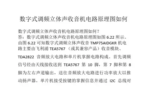
数字式调频立体声收音机电路原理图如何数字式调频立体声收音机电路原理图如何?答:数字式调频立体声收音机电路原理图如图6.22所示。
由图6.22可知数字式调频立体声收音TMP75AIDGKR机电路主要由飞利浦TEA5767 (或其兼容产品)收音模块、TDA2822音频放大电路和单片机掌握电路构成。
首先调频信号经由天线接收送到TEA5767第10脚,第7脚和第8 脚为左右声道输出,送往音频放大电路进行功率放大以推动扬声器。
单片机接受按键的掌握信息并通过I2C总线对TEA5767实现掌握,完成选台的功能,然后将频率实时显示在数码管上。
制作数字式调频立体声收音机需要选用哪些元器件?答:制作数字式调频立体声收音机需要选用4块集成电路, 其中∣C.选用STC89C51型单片机,IC,选用飞利浦TEA5767 型收音集成电路,IC,选用TDA2822型音频功率放大集成电路,IC。
选用7805型三端稳压集成电路。
vτ, ~vT,、VT,选用SC9012 型三极管,VT。
选用SC9014型三极管。
VD1、VD,、VDo 选用IN4148 型二极管,VD2〜VD5 选用1N4007型整流二极管,VD。
、VDo〜VD.,选用LED发光二极管。
晶体振荡器选用频率为11.0592MHz品振,其他元器件无特别要求,按图6.22所示型号选用。
制作数字式调频立体声收音机所用的元器件实物如图6.23所示。
数字式调频立体声收音机电路原理图如何?答:数字式调频立体声收音机电路原理图如图6.22所示。
由图6.22可知数字式调频立体声收音TMP75AIDGKR机电路主要由飞利浦TEA5767 (或其兼容产品)收音模块、TDA2822音频放大电路和单片机掌握电路构成。
首先调频信号经由天线接收送到TEA5767第10脚,第7脚和第8 脚为左右声道输出,送往音频放大电路进行功率放大以推动扬声器。
单片机接受按键的掌握信息并通过I2C总线对TEA5767实现掌握,完成选台的功能,然后将频率实时显示在数码管上。
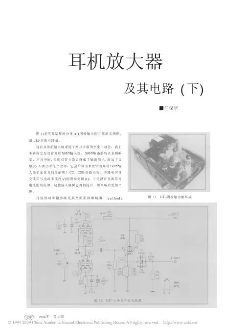
■任保华图11OTL阴极输出胆耳放图12OTL电子管耳放电路图耳机放大器及其电路(下)图11是笔者制作的分体OTL阴极输出胆耳放的实物图,图12是它的电路图。
这台耳放的输入级采用了两只并联的孪生三极管,我们不妨称它为双管并联SRPP输入级。
SRPP电路的特点是频响宽、声音华丽,采用双管并联后降低了输出阻抗,提高了灵敏度,不要小看这个改动,它会给你带来比常规单管SRPP输入级更加优良的性能呢!C2、C3是旁路电容。
旁路电容使交流信号电流不流经V1的阴极电阻R1,于是没有交流信号电流的负反馈,这使输入级瞬态得到提升、频率响应更加平坦。
耳放的功率输出级是典型的阴极跟随器(cathode图14变压器输出胆耳放图13变压器输出胆耳放电路图专题follower),或称阴极输出器。
阴极输出器过去曾经有过一段为声频爱好者狂热追求的历史,在那个时期各种杂志一片赞赏美誉之辞,声称如果把这种电路应用于声频放大器输出级,那么放大器就不会有非线性失真,频率特性会变得异常平坦,扬声器的阻尼问题也可得到很好的解决等等。
一时间阴极输出器似乎成了高保真设备的规范模式了。
日月荏苒,白驹过隙,随着时光的流逝这种电路却不知不觉地被人们淡忘了,在主流的胆机功放中已经很难找到它的身影。
那么阴极输出功率放大器是不是已经失去了昔日的风采了呢?当然不是。
我们知道,阴极输出器的基本特征是:1)高的动态输入阻抗;2)低的输出阻抗;3)通带电压放大系数小于1。
阴极输出器具有这些性能是因为它是一个电压负反馈放大器,所有电压负反馈放大器的优点,如噪声的抑低、频率响应性能的改善,非线性失真的抑低等等,它都具备。
阴极输出功率放大器的致命弱点是它的功率灵敏度太低,要求的输入电压幅度太大,对于前级来说,向后级供给很大的输入电压就可引起很大的非线性失真。
从总体上来讲会得不偿失,另一方面它的输出功率太小,效率很低;高阻抗的优质扬声器的匮乏也是影响阴极输出功率放大器发展的瓶颈。
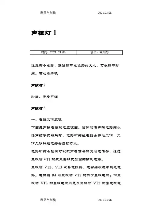
声控灯1这里有个电路,通过调节电位器的大小,可以调节时间。
可以参考哦声控灯2时间、亮度可调声控灯3一、电路工作原理下图是声控电路的电原理图。
当你对着声控电路的小话筒拍手或喊叫时,电路中的继电器会开始工作,工作几秒钟继电器会自动停止。
电路中的小话筒可以把声音信号转变为电信号,通过三极管VT1的放大去触发后面的控制电路。
三极管VT2、VT3及其电阻器、电容器组成单稳态电路。
电阻器R4为三极管VT2提供了基极电流;而三极管VT3的基极电流则是从三极管VT2的集电极电阻R5上得到的。
三极管VT2集电极与三极管VT3基极之间是直接耦合的;而三极管VT3集电极与三极管VT2基极之间的耦合则是由电容器C3来完成的。
单稳态电路的特点是它只有一个稳定状态。
电路在没有信号输入时,选择合理的R4阻值,使三极管VT2稳定在饱和状态;此时它的集电极电压约为0.3V以下。
这样使三极管VT3稳定在截止状态。
这就是单稳态电路的稳定状态。
当信号中的一个负脉冲通过C2到达三极管VT2的基极时,三极管VT2开始趋向截止,它的集电极电流减小,集电极电压升高;经过直接耦合,使三极管VT3的基极电压升高,三极管VT3开始导通,它的集电极电压下降;经电容C3的耦合又使三极管VT2的基极电压进一步下降(虽然这时负脉冲已经不再存在),形成一个正反馈,很快达到一个新的状态。
此时三极管VT2截止,三极管VT3饱和导通。
这就是单稳态电路的暂稳态现象。
单稳态电路的暂稳态是不能持久的。
在暂稳态期间,电容器C3通过电阻器R4进行放电,随着放电的进行三极管VT2的基极电压逐渐升高,当它达到0.5V以上时,三极管VT2开始导通,正反馈现象再次发生,整个电路很快又回到VT2饱和导通,VT3截止的稳定状态。
电容器C3通过电阻器R4的放电过程决定了电路暂稳态的维持时间。
根据计算,这个时间t—0.7×R4×C3。
在本电路中电阻R4为270kΩ,电容C3为47μF,所以t=0.7×270×103×47×10-6~9秒。
PWM的工作原理脉宽调制PWM是开关型稳压电源中的术语。
这是按稳压的控制方式分类的,除了PWM 型,还有PFM型和PWM、PFM混合型。
脉宽宽度调制式(PWM)开关型稳压电路是在控制电路输出频率不变的情况下,通过电压反馈调整其占空比,从而达到稳定输出电压的目的。
随着电子技术的发展,出现了多种PWM技术,其中包括:相电压控制PWM、脉宽PWM法、随机PWM、SPWM法、线电压控制PWM等,而在镍氢电池智能充电器中采用的脉宽PWM法,它是把每一脉冲宽度均相等的脉冲列作为PWM波形,通过改变脉冲列的周期可以调频,改变脉冲的宽度或占空比可以调压,采用适当控制方法即可使电压与频率协调变化。
可以通过调整PWM的周期、PWM的占空比而达到控制充电电流的目的。
pwm的定义脉宽调制(PWM)是利用微处理器的数字输出来对模拟电路进行控制的一种非常有效的技术,广泛应用在从测量、通信到功率控制与变换的许多领域中。
模拟信号的值可以连续变化,其时间和幅度的分辨率都没有限制。
9V电池就是一种模拟器件,因为它的输出电压并不精确地等于9V,而是随时间发生变化,并可取任何实数值。
与此类似,从电池吸收的电流也不限定在一组可能的取值范围之内。
模拟信号与数字信号的区别在于后者的取值通常只能属于预先确定的可能取值集合之内,例如在{0V, 5V}这一集合中取值。
模拟电压和电流可直接用来进行控制,如对汽车收音机的音量进行控制。
在简单的模拟收音机中,音量旋钮被连接到一个可变电阻。
拧动旋钮时,电阻值变大或变小;流经这个电阻的电流也随之增加或减少,从而改变了驱动扬声器的电流值,使音量相应变大或变小。
与收音机一样,模拟电路的输出与输入成线性比例。
尽管模拟控制看起来可能直观而简单,但它并不总是非常经济或可行的。
其中一点就是,模拟电路容易随时间漂移,因而难以调节。
能够解决这个问题的精密模拟电路可能非常庞大、笨重(如老式的家庭立体声设备)和昂贵。
模拟电路还有可能严重发热,其功耗相对于工作元件两端电压与电流的乘积成正比。
Ver 1.0 2000.01WM-FX491/FX491ST/FX493/FX493STRADIO CASSETTE PLAYERSPECIFICATIONSUS ModelWM-FX493/FX493STCanadian ModelWM-FX491/FX491ST/FX493STAEP Model E Model Chinese ModelWM-FX491/FX493Model Name Using Similar Mechanism WM-FX477Tape T ransport Mechanism TypeMT -WMEX404-147Photo : WM-FX493SERVICE MANUAL• Frequency range FM:87.5–108 MHzAM:530–1710 kHz (US, Canadian, 5E, 6E model)531–1602 kHz (EXCEPT US, Canadian, 5E, 6E model)• Power requirements3 V DC batteries R6 (size AA) x 2• Dimensions (w/h/d)Approx. 115.8 x 83.2 x 30.1 mm, incl. projecting parts and controls • MassApprox. 115 g/Approx. 195 g (incl. a battery and a cassette)• Supplied accessoriesStereo headphones or earphones with remote control (1)(FX493/FX493ST)/Stereo headphones or earphones (1)(FX491/FX491ST)Design and specifications are subject to change without notice.•Abbreviation5E, 6E :South AmericaBattery life (approximate hours) (EIAJ*)Sony alkaline LR6 (SG)Sony R6P (SR)Tape playback 257.5Radio reception 4014*Measured value by the standard of EIAJ (ElectronicIndustries Association of Japan). (Using a Sony HF series cassette tape)Note•The battery life may shorten depending on the operation of the unit.TABLE OF CONTENTS Specifications (1)1.GENERALLocation and Function of Controls (3)2.DISASSEMBL Y2-1. Cabinet (Front) Sub ASSY (5)2-2. Main Board (5)2-3. Mechanism Deck (6)2-4. Belt, Motor (Capstan/Reel) (M901) (6)2-5. “Holder Sub ASSY, Cassette” (7)3.ADJUSTMENTS3-1. Mechanical Adjustments (8)3-2. Electrical Adjustments (8)4.DIAGRAMS4-1. Explanation of IC Terminals (11)4-2. Block Diagram (13)4-3. Printed Wiring Boards (15)4-4. Schematic Diagram (19)5.EXPLODED VIEWS5-1. Cabinet Section (23)5-2. Mechanism Deck Section (MT-WMEX404-147) (24)6.ELECTRICAL PARTS LIST (25)Flexible Circuit Board Repairing•Keep the temperature of the soldering iron around 270°C during repairing.•Do not touch the soldering iron on the same conductor of the circuit board (within 3 times).•Be careful not to apply force on the conductor when soldering or unsoldering.Notes on chip component replacement•Never reuse a disconnected chip component.•Notice that the minus side of a tantalum capacitor may be dam-aged by heat.– 2 –– 3 –SECTION 1GENERALLOCATION AND FUNCTION OF CONTROLSThis section is extracted from instruction manual.ABCFX493FX491– 4 –Listening to the Radio B1If the HOLD function is turned on, slide the HOLD switch in the opposite direction of the arrow to unlock the controls.2Press RADIO ON/BAND to turn on the radio.3Press RADIO ON/BAND repeatedly to select AM, FM1, FM2 or FM3.4Press TUNING +/– to tune in to the desired station.If you keep pressing TUNING+/– for a few seconds, the Walkman will start tuning to the stations automatically.To turn off the radioPress x •RADIO OFF.To improve the broadcast reception C• For FM: Extend the headphones/earphones cord (antenna) (FX491) or remote control cord (antenna)(FX493). If the reception is still not good, pressMENU repeatedly to set the cursor to FM MODE in the display.• For AM: Reorient the unit itself.Presetting Radio StationsYou can store radio stations into the unit’s memory.You can preset up to 32 radio stations, 8 for each FM1, FM2, FM3 or AM bands.1Press RADIO ON/BAND to turn on the radio.2Press RADIO ON/BAND repeatedly to select AM, FM1, FM2 or FM3.3Press ENTER.The frequency digits and a preset number flash in the display.4While the frequency digits and the preset number are flashing, tune in to a station you wish to store using TUNING+/–, and select a preset number using PRESET+/–.5While the frequency digits and the preset number are flashing, press ENTER.Notes•If you cannot complete step 4 or 5 while the indications are flashing, repeat from step 3.•If a station is already stored, the new station replaces the old one.To cancel the stored stationFollow the procedure above and in step 3, instead of tuning in to a station, press and hold TUNING +/– until “- - - -” is displayed. Press ENTER while “- - - -” is flashing.To play the preset radio stations1Press RADIO ON/BAND to select the band.2Press PRESET+/–.To operate from the remote control (FX493 only)To turn on the radio, press RADIO ON/BAND•OFF for more than one second (only while the tape is in stop mode).To select the band, press RADIO ON/BAND•OFF for more than one second while the radio is on.To tune in or recall a preset station, press PRESET +or –.To turn off the radio, press RADIO ON/BAND•OFF.Using Other FunctionsTo lock the controlsSet the HOLD switch to the direction of the arrow to lock the controls.PreparationsTo Insert Batteries A1Slide and open the battery compartment lid,and insert two R6 (size AA) dry batteries with correct polarity.Replace the batteries with new ones when " e "flashes in the display.Playing a Tape B1If the HOLD function is turned on, slide the HOLD switch in the opposite direction of the arrow to unlock the controls.2Insert a cassette and press MENUrepeatedly to set the cursor to TAPE in the display. Then press SET to select the tape type.No message: normal (TYPE I)METAL: CrO 2 (TYPE II) or metal (TYPE IV)3Press Y on the main unit, or if using the remote control (FX493 only), press Y (play)•x (stop).Adjust the volume with VOL.When adjusting the volume on the Walkman (FX493only)Set the VOL control on the remote control at maximum.When adjusting the volume on the remote control (FX493 only)Set the VOL control on the Walkman slightly above the appropriate level.Note on the cassette holderWhen opening the cassette holder, press the x (stop)button and make sure the tape is stopped by checking through the cassette window, then slide the OPEN switch.If the cassette holder is opened before the tape is stopped, the tape may loosen and be damaged.Operation on the main unitT oSwitch playback to the other side Stop playbackOperation on the remote control (FX493only)T oSwitch playback to the other side Stop playbackOther tape operationsT oFast forward*Rewind*Play the same side from the beginning (Auto Play function)Play the other side from the beginning (Skip Reverse function)*For FX493 only: If Y •x on the remote control is pressed during fast forward or rewind, the Walkman switches to playback.To select playback modePress MENU repeatedly to set the cursor to MODE in the display.Then press SET to select the desired mode.To playBoth sides repeatedly Both sides once from the side facing the cassette holderPressY •x for 2 seconds or more during playback Y •x once during playbackPressY (play)during playback xSelect s dPress FF during stop REW during stopREW during playback FF during playback To emphasize bass soundPress MENU repeatedly to set the cursor to MB in the display. Then, press SET to turn MB on. With each press, the indications change as follows.MB (MEGA BASS) : emphasizes bass sound No message: off (normal)Notes•If the sound is distorted with the mode “MB”, turn down the volume of the main unit or select normal mode.•Bass emphasis may not show great effect if the volume is turned up too high.To protect your hearing—AVLS(Automatic Volume Limiter System)functionWhen you set the AVLS function to active, themaximum volume is kept down to protect your ears.Note•The AVLS setting will be canceled when you replace the batteries.– 5 –SECTION 2DISASSEMBLYNote : Follow the disassembly procedure in the numerical order given.2-1. CABINET (FRONT) SUB ASSY2-2. MAIN BOARDz The equipment can be removed using the following procedure.Main boardHolder sub ASSY, CassetteBelt, Motor (Capstan/reel) (M901)Set5Main boardRemove solder– 6 –2-3. MECHANISM DECK2-4. BELT, MOTOR (CAPSTAN/REEL) (M901)11 belt3 Motor (Capstan/reel) (M901)wheel assy (SP), capstanbelt• How to apply the beltM9012 Screws (M1.4)3 Move hinge away 51Insert the spring (Lid up) to the slot as shown in the figure.23 Insert the hinge of the “Holder sub ASSY , Cassette”.4Close the “Holder sub ASSY , Cassette” then press it.2-5. “HOLDER SUB ASSY, CASSETTE”z CAUTIONS DURING ASSEMBL Y– 8 –3-1. MECHANICAL ADJUSTMENTSPRECAUTION1.Clean the following parts with a denatured-alcohol-moistened swab :playback head pinch roller capstan rubber belt2.Demagnetize the playback head with a head demagnetizer.Do not use a magnetized screwdriver for the adjustments.3.These measurement and adjustment should be performed with the rated power supply voltage (2.5 V) unless otherwise noted.Torque MeasurementMode Torque meterMeter reading FWD 20 – 42 g • cm CQ-102C (0.28 – 0.58 oz• inch)FWDless than 2 g • cm back tension (less than 0.027 oz• inch)REV 20 – 42 g • cm CQ-102RC (0.28 – 0.58 oz• inch)REVless than 2 g • cm back tension (less than 0.027 oz• inch)FF, REWCQ-201Bmore than 60 g • cm (more than 0.84 oz• inch)SECTION 3ADJUSTMENTS3-2. ELECTRICAL ADJUSTMENTSPRECAUTION•Supplied voltage : 2.5V .•Switch and control position MEGA BASS : OFFVOLUME control : maximum A VLS : NORMTAPE SECTIONTest TapeT ype Signal Used for WS-48A3kHz, 0dBTape Speed AdjustmentTape Speed Adjustment Procedure :1.Playback WS-48A (tape center part) in the FWD state and ad-just RV601 so that the frequency counter reading becomes 3,000Hz.Standard value : 2,985–3,015Hz2.Playback WS-48A (tape center part) in the REV state.Check that frequency counter reading is within ±1.0% of the reading of step 1.Adjustment Location :0 dB = 0.775Vtest tape WS-48A frequency counter RV601– 9 –– 10 –Adjustment Location :Frequency Coverage Adjustment Setting :digital voltmeter (DC range)L4 : AM Frequency Coverage AdjustmentL3 : FM Frequency Coverage Adjustment4-2. BLOCK DIAGRAM•Signal path. F: FM f: AM E: PB •AbbreviationCND:CanadianEA:Saudi ArabiaCH: Chinese9E:Indication of country of origin 5E, 6E:South AmericaSECTION 4 DIAGRAMS4-1. EXPLANATION OF IC TERMINALSIC701 TC9327AF-621 (SYSTEM CONTROL/LCD DRIVE)Pin No.Pin Name I/O Pin Description1– 4COM1 – 4O LCD driver common output.5 – 22S1 – 18O LCD driver output.23MOTOR DIR O Motor rotation direction control output (FWD: L, REV: H).24MOTOR CTL O Motor ON/OFF control output (OFF: L, ON: H).25MOTOR SPEED O Motor speed control output (Normally: L, Speed down: H).26MOTOR BRK O Motor brake control output (Brake OFF: L, Brake ON: H).27PHOTO CTL O Photo reflector rotation detection control output.28DOLBY—Not used (OPEN).29NC—Not used (OPEN).30A VLS O A VLS control output (A VLS OFF: L, A VLS IN: H).31FM MODE O LOCAL/DX control output (DX: L, LOCAL: H) (US, CND, 5E, 6E only).32TAPE SELECT O Tape select control output (Normal: L, CrO2/METAL: H).33PHOTO IN I Photo reflector rotation detection input.34 – 37K0 – 3I Key input 0 – 3.38NC—Not used (OPEN).39 – 41KO1 – 3I Key input 1 – 3.42BATT DET I Power supply voltage detection input (A/D input).43HOLD I HOLD input.44RM KEY IN I Remote control key input.45AD REF I Reference voltage of pin 43 and 44.46CS O Chip select output for EEPROM.47DATA O Data output for EEPROM.48SCLK O SCLK output for EEPROM.49BEEP O BEEP output.50TEST I Test mode select terminal (Connect to remote contorol).51MEGA BASS O MEGA BASS control output (ON: L, OFF: H).52MUTE O Mute signal output (OFF: L, ON: H)53AMP CTL O Power AMP ON/OFF control output.54OPEN I OPEN switch input.55REV SW I Mechanism deck mode detection switch input (REV ON: H).56REW SW I Mechanism deck mode detection switch input (REW ON: H).57FF SW I Mechanism deck mode detection switch input (FF ON: H).58FWD SW I Mechanism deck mode detection switch input (FWD ON: H).59BAND O BAND select output (AM: L, FM: input).60RADIO ON O RADIO ON/OFF control output (OFF: L, ON: H).61IF REQ O IF request output (Auto scan: L, Normally: H).62NC—Not used (OPEN).63TEST/NC—Not used (OPEN).64IF IN I IF input.65PRE AMP CTL O Preamp mute signal output.66D02O VT control signal output.67HOLD—Fixed at “H” in this set.68NC—Not used (OPEN).69GND—Ground.70VCO FM I VCO (FM) input.Pin No.Pin Name I/O Pin Description71VCO AM I VCO (AM) input.72VDD—Power supply pin.73RESET I Reset input. Connect to VDD.74XOUT O Crystal oscillator output (75 kHz).75XIN I Crystal oscillator input (75 kHz).76VXT—Stabilized capacitor connection of crystal oscillation power supply.77VLCD—LCD driver power rising pressure pin.78, 79C1, 2—LCD driver power rising pressure pin.80VEE— 1.5 V constant voltage power supply for LCD driver.WM-FX491/FX491ST/FX493/FX493STWM-FX491/FX491ST/FX493/FX493STNote:•X : parts extracted from the component side.•a : Through hole.•b : Pattern from the side which enables seeing.(The other layers' patterns are not indicated.) Caution:Pattern face side:Parts on the pattern face side seen from the (Side B)pattern face are indicated.Parts face side:Parts on the parts face side seen from the (Side A)parts face are indicated.•AbbreviationCND :Canadian FR :French EA :Saudi Arabia CH : Chinese E :Indication of country of origin 9E :No Indication of country of origin 5E, 6E:South AmericaCEV :Ukraine, Hungary, Czech4-3. PRINTED WIRING BOARDSD1C-18D2C-4D3C-4D301B-19D401E-14D402E-14IC1D-3IC101D-9IC701C-14IC702B-17IC703C-15Q2C-3Q51B-13Q52B-13Q53B-13Q303E-4Q304B-12Q305B-13Q401D-14Q603B-4Q604C-11Q605C-11Q606C-12Q607C-11Q701E-14Q702E-7Q703B-15Q751B-14Q752B-14Ref. No.Location z SemiconductorLocation4-4. SCHEMATIC DIAGRAMNote:•All capacitors are in µF unless otherwise noted. pF: µµF 50 WV or less are not indicated except for electrolytics and tantalums.•All resistors are in Ω and 1/4 W or less unless otherwise specified.•f : internal component.•U : B+ Line.•H : adjustment for repair.•Power voltage is dc 3V and fed with regulated dc power supply from battery terminal.•Voltages and waveforms are dc with respect to ground under no-signal (detuned) conditions.no mark : FM (RADIO SECTION)PLAY (TAPE SECTION)(): AM•Voltages are taken with a VOM (Input impedance 10 M Ω).Voltage variations may be noted due to normal produc-tion tolerances.•Waveforms are taken with a oscilloscope.Voltage variations may be noted due to normal produc-tion tolerances.•Circled numbers refer to waveforms.•Signal path.F : FM f : AM E : PB •AbbreviationCND :Canadian FR :French EA :Saudi Arabia CH : Chinese E :Indication of country of origin 9E :No Indication of country of origin 5E, 6E:South AmericaCEV :Ukraine, Hungary, Czechz Waveformsz Refer to page 22 for IC Block Diagram.WM-FX491/FX491ST/FX493/FX493STz IC Block Diagram.IC1 TA2104AFN (EL)F M R F O U TR F V C CA M R F I NF M O S CA M O S CO S C O U TS T -L E DI F R E QD E T O U TM P X -I NL P F 1/M O -S TL P F 2/B A N DR F G N DF M R F I NA M L O W C U TM I X O U TV C CA M I F I NF M I F I NG N DA G CQ U A DR -O U TL -O U TSECTION 5EXPLODED VIEWSNOTE :•-XX, -X mean standardized parts, so they may have some difference from the original one.•Items marked “ * ”are not stocked since they are seldom required for routine service. Some delay should be anticipated when ordering these items.•The mechanical parts with no reference number in the exploded views are not supplied.•Hardware (# mark) list and accessories and packing materials are given in the last of this parts list.•Abbreviation CND :Canadian FR :French EA :Saudi Arabia CH : Chinese E :Indication of country of origin 9E :No Indication of country of origin 5E, 6E :South America5-2. MECHANISM DECK SECTION (MT -WMEX404-147)5352525471565571575859607061626869M90163646666676769686551HP901Ref. No.Part No.DescriptionRemarkRef. No.Part No.DescriptionRemark13-039-652-01LID,BATTERY CASE (FX491,FX491ST)13-039-652-11LID,BATTERY CASE (FX493,FX493ST)23-039-658-01RUBBER (B), BUTTON3X-3378-293-1CABINET (FRONT) SUB ASSY(FX491,FX491ST)3X-3378-294-1CABINET (FRONT) SUB ASSY(FX493,FX493ST)43-039-657-01RUBBER (A), BUTTON 53-704-197-11LOCK,SERRAT IB *63-039-660-01HOLDER (LCD)73-040-176-01RUBBER, CONDUCTIVE 83-022-857-01SPRING (OPEN)93-022-856-01SPRING (KNOB), TENSION 103-704-197-91SCREW (M1.4X1.8), LOCKING 113-019-421-01LEVER, OPEN 123-019-422-01JOINT 133-349-825-31SCREW143-318-382-61SCREW (1.7X2.5), TAPPING 153-039-661-01LOCKER (OPEN)163-025-276-01SPRING (LID UP)17X-3378-289-1HOLDER SUB ASSY, CASSETTE(FX491:CND,5E,6E,FX491ST)17X-3378-290-1HOLDER SUB ASSY, CASSETTE(FX491:AEP,CEV,FR,E,9E,CH)17X-3378-291-1HOLDER SUB ASSY, CASSETTE(FX493:US,5E,6E,FX493ST)17X-3378-292-1HOLDER SUB ASSY, CASSETTE(FX493:AEP ,CEV,FR,9E,EA,CH)183-019-514-21KNOB(OPEN)193-039-651-01CENTER CABINET (US,CND,5E,6E)193-039-651-11CENTER CABINET (E,EA,CH)193-039-651-21CENTER CABINET (AEP ,CEV,FR)193-039-651-31CENTER CABINET (9E)203-318-203-51SCREW (B1.7X12), TAPPING 213-040-144-01SPRING (CASSETTE)233-020-511-01TERMINAL (+), BATTERY24A-3021-309-A MAIN BOARD, COMPLETE (US,CND)24A-3021-310-A MAIN BOARD, COMPLETE (AEP ,CEV)24A-3021-311-A MAIN BOARD, COMPLETE (E,9E,EA,CH)24A-3021-312-A MAIN BOARD, COMPLETE (5E,6E)24A-3021-313-AMAIN BOARD, COMPLETE (FR)253-020-512-01TERMINAL (-), BATTERYL21-501-987-21AM FERRITE-ROD ANTENNA (AM TRACKING)ND7011-803-764-11DISPLAY PANEL, LIQUID CRYSTALRef. No.Part No.DescriptionRemarkRef. No.Part No.DescriptionRemark51X-3375-020-1PINCH LEVER (N-F) ASSY 52X-3372-619-1WHEEL ASSY (SP), CAPSTAN 533-354-868-01BELT543-021-950-01GEAR (DF)553-021-982-01SPRING (MODE), COMPRESSION 56X-3375-024-1CLUTCH ASSY (F)573-021-951-01GEAR (CAM)583-348-953-21WASHER593-021-979-01SPRING (UDF), COMPRESSION 603-021-949-01GEAR (BF)61X-3375-022-1CHASSIS ASSY (F)623-021-974-03SPRING (HEAD BASE)633-703-816-31SCREW (M1.4), SPECIAL HEAD 64X-3375-021-1PINCH LEVER (R-F) ASSY653-703-816-73SCREW (M1.4), SPECIAL HEAD 663-921-797-01WASHER 673-921-003-01BEARING683-022-100-01SPRING (B.T.), COMPRESSION 693-024-223-01GEAR (REEL-2)70X-3375-268-1GEAR (AF-SV) ASSY713-034-685-01WASHER (1.03-3.0)HP9011-500-555-11HEAD, MAGNETIC (PLAYBACK)M9011-763-073-11MOTOR, DC (CAPSTAN/REEL)(INCLUDING PULLEY)NOTE :•Due to standardization, replacements in the parts list may be different from the parts specified in the diagrams or the components used on the set.•-XX, -X mean standardized parts, so they may have some difference from the original one.•RESISTORSAll resistors are in ohms METAL : Metal-film resistorMETAL OXIDE :Metal oxide-film resistor F : nonflammable•Items marked “ * ”are not stocked since they are seldom required for routine service.Some delay should be anticipated when ordering these items.•SEMICONDUCTORSIn each case, u : µ, for example :uA.... : µA.... , uPA.... : µPA....uPB.... : µPB.... , uPC.... : µPC....uPD.... : µPD....•CAPACITORS uF : µF •COILS uH : µHWhen indicating parts by reference num-ber, please include the board.SECTION 6ELECTRICAL PARTS LISTRef. No.Part No.DescriptionRemark Ref. No.Part No.DescriptionRemark •Abbreviation CND :Canadian FR :French EA :Saudi Arabia CH : Chinese E :Indication of country of origin 9E :No Indication of country of origin 5E, 6E :South AmericaCEV :Ukraine, Hungary, CzechA-3021-309-A MAIN BOARD, COMPLETE (US,CND)A-3021-310-A MAIN BOARD, COMPLETE (AEP ,CEV)A-3021-311-A MAIN BOARD, COMPLETE (E,EA,9E,CH)A-3021-312-A MAIN BOARD, COMPLETE (5E,6E)A-3021-313-AMAIN BOARD, COMPLETE (FR)*********************3-020-511-01TERMINAL (+), BATTERY 3-020-512-01TERMINAL (-), BATTERY *3-039-660-01HOLDER (LCD)3-040-176-01RUBBER, CONDUCTIVE < CAPACITOR >C11-115-416-11CERAMIC CHIP 1000PF 5%25V C21-162-959-11CERAMIC CHIP 330PF 5%50V C31-162-995-11CERAMIC CHIP 0.022uF 50VC41-162-907-11CERAMIC CHIP 2PF 0.25PF 50VC51-162-995-11CERAMIC CHIP 0.022uF 50VC61-164-156-11CERAMIC CHIP 0.1uF 25V C71-162-919-11CERAMIC CHIP 22PF 5%50V C81-162-959-11CERAMIC CHIP 330PF 5%50V C91-163-033-91CERAMIC CHIP 0.022uF 50V C101-115-416-11CERAMIC CHIP 1000PF 5%25V C111-115-416-11CERAMIC CHIP 1000PF 5%25V C121-162-915-11CERAMIC CHIP 10PF 0.5PF 50V C131-162-970-11CERAMIC CHIP 0.01uF 10%25V C141-162-909-11CERAMIC CHIP 4PF 0.25PF 50V C151-162-970-11CERAMIC CHIP 0.01uF 10%25V C161-115-416-11CERAMIC CHIP 1000PF 5%25V C171-115-156-11CERAMIC CHIP 1uF 10V C181-107-826-91CERAMIC CHIP 0.1uF 10%16V C191-109-982-11CERAMIC CHIP 1uF 10%10V C201-164-156-11CERAMIC CHIP0.1uF25VC211-162-970-11CERAMIC CHIP 0.01uF 10%25V(EXCEPT US,CND,5E,6E)C211-164-245-11CERAMIC CHIP 0.015uF 10%25V(US,CND,5E,6E)C221-162-970-11CERAMIC CHIP 0.01uF 10%25V(EXCEPT US,CND,5E,6E)C221-164-245-11CERAMIC CHIP 0.015uF 10%25V(US,CND,5E,6E)C231-125-837-91CERAMIC CHIP 1uF 10% 6.3V C241-125-837-91CERAMIC CHIP 1uF 10% 6.3V C251-109-935-11TANTAL. CHIP 4.7uF 20%4V C261-162-974-11CERAMIC CHIP0.01uF50VC281-162-974-11CERAMIC CHIP 0.01uF 50V C291-115-467-11CERAMIC CHIP 0.22uF 10%10VC301-163-275-11CERAMIC CHIP 0.001uF 5%50V C311-113-988-11TANTAL. CHIP 68uF 20%4V C321-164-315-11CERAMIC CHIP 470PF 5%50V C331-115-416-11CERAMIC CHIP1000PF 5%25V (US,CND,5E,6E)C341-164-315-11CERAMIC CHIP 470PF 5%50V C351-162-970-11CERAMIC CHIP 0.01uF 10%25V C361-162-970-11CERAMIC CHIP 0.01uF 10%25V C371-162-970-11CERAMIC CHIP 0.01uF 10%25V C401-162-921-11CERAMIC CHIP 33PF 5%50V C411-115-416-11CERAMIC CHIP 1000PF 5%25V C511-162-964-11CERAMIC CHIP 0.001uF 10%50V C521-104-847-11TANTAL. CHIP 22uF 20%4V C531-162-970-11CERAMIC CHIP 0.01uF 10%25V C1071-115-156-11CERAMIC CHIP 1uF 10V C2051-115-156-11CERAMIC CHIP 1uF 10V C2071-115-156-11CERAMIC CHIP 1uF 10V C3051-124-433-00ELECT100uF 20%4V C3111-107-826-91CERAMIC CHIP 0.1uF 10%16V C3121-107-826-91CERAMIC CHIP 0.1uF 10%16V C3131-115-416-11CERAMIC CHIP 1000PF 5%25V C4011-115-416-11CERAMIC CHIP 1000PF 5%25V C4021-164-505-11CERAMIC CHIP 2.2uF 16V C4031-162-915-11CERAMIC CHIP 10PF 0.5PF 50V C4041-162-915-11CERAMIC CHIP 10PF 0.5PF 50VC4051-104-847-11TANTAL. CHIP 22uF 20% 4VC4061-162-974-11CERAMIC CHIP 0.01uF 50V C4071-162-974-11CERAMIC CHIP 0.01uF 50V C6081-107-826-91CERAMIC CHIP 0.1uF 10%16V C6101-124-434-00ELECT220uF 20%4V C7011-162-974-11CERAMIC CHIP 0.01uF 50V C7021-104-847-11TANTAL. CHIP 22uF 20%4V C7041-162-964-11CERAMIC CHIP 0.001uF 10%50V C7051-115-467-11CERAMIC CHIP 0.22uF 10%10V C7061-162-927-11CERAMIC CHIP 100PF 5%50V C7071-162-927-11CERAMIC CHIP 100PF 5%50V C7081-115-416-11CERAMIC CHIP 1000PF 5%25V C7091-162-927-11CERAMIC CHIP 100PF 5%50V C7101-162-974-11CERAMIC CHIP 0.01uF 50V C7121-162-917-11CERAMIC CHIP 15PF 5%50V C7131-162-917-11CERAMIC CHIP15PF5%50VMAINC7141-115-156-11CERAMIC CHIP1uF10VC7151-164-156-11CERAMIC CHIP0.1uF25VC7161-164-156-11CERAMIC CHIP0.1uF25VC7171-164-156-11CERAMIC CHIP0.1uF25VC7181-115-416-11CERAMIC CHIP1000PF5%25VC7191-115-416-11CERAMIC CHIP1000PF5%25VC7201-115-416-11CERAMIC CHIP1000PF5%25VC7211-115-416-11CERAMIC CHIP1000PF5%25VC7221-115-416-11CERAMIC CHIP1000PF5%25VC7231-115-416-11CERAMIC CHIP1000PF5%25VC7241-115-416-11CERAMIC CHIP1000PF5%25VC7251-115-416-11CERAMIC CHIP1000PF5%25V< FILTER >CF11-781-271-11FILTER, CERAMICCF21-781-152-11FILTER, CERAMIC< CONNECTOR >CN3031-750-346-21CONNECTOR, FFC/EPC (ZIF) 6P< TRIMMER >CT11-141-463-11CAP, ADJ 10PF (AM TRACKING)< DIODE >D18-719-053-30DIODE MA2S357-(TX). SOD28-719-072-58DIODE SVC347-TLD38-719-053-30DIODE MA2S357-(TX). SOD3018-719-017-58DIODE MA8068D4018-719-073-01DIODE MA111-(K8).S0D4028-719-056-89DIODE UDZ-TE-17-12B< FERRITE BEAD >FB21-500-113-22FERRITEFB1011-500-113-22FERRITEFB2011-500-113-22FERRITEFB3011-500-113-22FERRITEFB3111-500-113-22FERRITEFB3121-500-113-22FERRITEFB3131-500-113-22FERRITE< FILTER >FL11-236-711-21FILTER, BAND PASS< IC >IC18-759-564-18IC TA2104AFN(EL)IC1011-418-581-11EG UNIT (WFX)IC7018-759-653-11IC TC9327AF-621IC7028-759-457-70IC XC62RP1602MRIC7038-759-457-68IC AK93C45AV-L< JACK >J3011-785-164-11JACK (i)J3031-750-061-11JACK,DC(POLARITY UNIFIED TYPE)(DC IN 3V) (E,EA,9E,CH)< JUMPER RESISTOR >JC1011-216-296-00METAL CHIP05%1/8W JC1021-216-296-00METAL CHIP05%1/8W JC1031-216-864-11METAL CHIP05%1/16W JC1061-216-296-00METAL CHIP05%1/8W JC1071-216-296-00METAL CHIP05%1/8WJC1081-216-864-11METAL CHIP05%1/16W JC1091-216-295-00METAL CHIP05%1/10W JC1101-216-295-00METAL CHIP05%1/10W JC1111-216-296-00METAL CHIP05%1/8W< COIL >L11-416-596-11COIL (RF) (FM TRACKING)L21-501-987-21AM FERRITE-ROD ANTENNA (AM TRACKING) L31-416-595-11COIL (OSC) (FM FREQUENCY COVERAGE)L41-415-962-11COIL (OSC) (AM FREQUENCY COVERAGE)L4011-412-991-11INDUCTOR10uHL7011-412-995-21INDUCTOR22uHL7021-412-973-11INDUCTOR0.33uH<LIQUID CRYSTAL>ND7011-803-764-11DISPLAY PANEL, LIQUID CRYSTAL< PHOTO INTERRUPTER >PH7518-749-016-61REFLECTOR NJL5197K-W-F20(TE1)< TRANSISTOR >Q28-729-602-21TRANSISTOR 2SC4154-F (US,CND,5E,6E) Q518-729-420-24TRANSISTOR 2SB1218A-QRSQ528-729-402-13TRANSISTOR XN1501Q538-729-015-76TRANSISTOR UN5211Q3038-729-402-13TRANSISTOR XN1501Q3048-729-807-86TRANSISTOR 2SB1295-UL5Q3058-729-015-76TRANSISTOR UN5211Q4018-729-602-21TRANSISTOR 2SC4154-FQ6038-729-421-26TRANSISTOR UN5216Q6048-729-046-89TRANSISTOR 2SB970-S(TX).S0Q6058-729-046-89TRANSISTOR 2SB970-S(TX).S0Q6068-729-046-89TRANSISTOR 2SB970-S(TX).S0Q6078-729-421-26TRANSISTOR UN5216Q7018-729-602-21TRANSISTOR 2SC4154-FQ7028-729-231-96TRANSISTOR 2SK880GR-TE85LQ7038-729-423-55TRANSISTOR 2SC3931-DQ7518-729-421-26TRANSISTOR UN5216Q7528-729-420-24TRANSISTOR 2SB1218A-QRS< RESISTOR >R11-216-853-11METAL CHIP470K5%1/16W R21-216-853-11METAL CHIP470K5%1/16W R31-216-853-11METAL CHIP470K5%1/16W R41-216-821-11METAL CHIP1K5%1/16W R51-216-853-11METAL CHIP470K5%1/16W R61-216-853-11METAL CHIP470K5%1/16W R71-216-853-11METAL CHIP470K5%1/16W R81-216-864-11METAL CHIP05%1/16W R91-216-817-11METAL CHIP4705%1/16W R101-216-827-11METAL CHIP 3.3K5%1/16WMAINRef. No.Part No.Description Remark Ref. No.Part No.Description RemarkR111-216-296-91SHORT0R121-216-833-91RES-CHIP10K5%1/16W R131-216-821-11METAL CHIP1K5%1/16W R141-216-845-11METAL CHIP100K5%1/16W(EXCEPT US,CND,5E,6E) R151-216-827-11METAL CHIP 3.3K5%1/16WR161-216-821-11METAL CHIP1K5%1/16W R171-216-839-11METAL CHIP33K5%1/16W R181-216-839-11METAL CHIP33K5%1/16W R191-216-815-11METAL CHIP3305%1/16W R201-216-821-11METAL CHIP1K5%1/16W(US,CND,5E,6E)R211-216-864-11METAL CHIP05%1/16W R221-216-864-11METAL CHIP05%1/16W R521-216-819-11METAL CHIP6805%1/16W R531-216-829-11METAL CHIP 4.7K5%1/16W R541-216-847-11METAL CHIP150K5%1/16WR551-216-833-91RES-CHIP10K5%1/16W R1001-216-864-11METAL CHIP05%1/16W(EXCEPT E,EA,9E,CH) R1071-216-791-11METAL CHIP 3.35%1/16W(US,CND) R1071-216-797-11METAL CHIP105%1/16W(EXCEPT US,CND,FR) R1071-216-811-11METAL CHIP1505%1/16W(FR)R1081-216-811-11METAL CHIP1505%1/16W(EXCEPT US,CND,FR) R1081-216-817-11METAL CHIP4705%1/16W(US,CND,FR) R1091-216-825-11METAL CHIP 2.2K5%1/16W R2071-216-791-11METAL CHIP 3.35%1/16W(US,CND) R2071-216-797-11METAL CHIP105%1/16W(EXCEPT US,CND,FR)R2071-216-811-11METAL CHIP1505%1/16W(FR) R2081-216-811-11METAL CHIP1505%1/16W(EXCEPT US,CND,FR) R2081-216-817-11METAL CHIP4705%1/16W(US,CND,FR) R2091-216-825-11METAL CHIP 2.2K5%1/16W R3041-216-821-11METAL CHIP1K5%1/16W R3051-216-821-11METAL CHIP1K5%1/16W R3101-216-821-11METAL CHIP1K5%1/16W R4011-216-845-11METAL CHIP100K5%1/16W R4021-216-821-11METAL CHIP1K5%1/16W R4031-216-845-11METAL CHIP100K5%1/16WR4041-216-813-11METAL CHIP2205%1/16W R6061-216-845-11METAL CHIP100K5%1/16W R6081-216-827-11METAL CHIP 3.3K5%1/16W R6091-216-833-91RES-CHIP10K5%1/16W R6101-216-821-11METAL CHIP1K5%1/16W R6111-216-864-11METAL CHIP05%1/16W R6121-216-841-11METAL CHIP47K5%1/16W R6131-216-817-11METAL CHIP4705%1/16W R6141-216-817-11METAL CHIP4705%1/16W R6151-216-817-11METAL CHIP4705%1/16WR7001-216-829-11METAL CHIP 4.7K5%1/16W R7011-216-835-11METAL CHIP15K5%1/16WR7021-216-841-11METAL CHIP47K5%1/16W R7031-216-805-11METAL CHIP475%1/16W R7041-216-835-11METAL CHIP15K5%1/16WR7051-216-837-11METAL CHIP22K5%1/16W R7061-216-825-11METAL CHIP 2.2K5%1/16W R7071-216-864-11METAL CHIP05%1/16W R7081-216-845-11METAL CHIP100K5%1/16W R7111-216-821-11METAL CHIP1K5%1/16WR7151-216-853-11METAL CHIP470K5%1/16W R7221-216-821-11METAL CHIP1K5%1/16W R7231-216-821-11METAL CHIP1K5%1/16W R7241-216-821-11METAL CHIP1K5%1/16W R7261-216-833-91RES-CHIP10K5%1/16W R7271-216-833-91RES-CHIP10K5%1/16W R7281-216-833-91RES-CHIP10K5%1/16W R7291-216-833-91RES-CHIP10K5%1/16W R7511-216-817-11METAL CHIP4705%1/16W R7521-216-851-11METAL CHIP330K5%1/16WR7531-216-853-11METAL CHIP470K5%1/16W R7541-216-821-11METAL CHIP1K5%1/16W R7551-216-853-11METAL CHIP470K5%1/16W R7561-216-853-11METAL CHIP470K5%1/16W R7571-216-853-11METAL CHIP470K5%1/16W R7581-216-853-11METAL CHIP470K5%1/16W R7591-216-845-11METAL CHIP100K5%1/16W R7611-216-833-91RES-CHIP10K5%1/16W R7701-216-833-91RES-CHIP10K5%1/16W R7711-218-871-11METAL CHIP10K0.5%1/16W< VARIABLE RESISTOR >RV3011-225-362-11RES, VAR, CARBON (w VOL)RV6011-241-784-11RES, ADJ, CARBON 5K (TAPE SPEED)< SWITCH >S3011-771-040-21SWITCH, PUSH (OPEN DET)S6011-771-598-11SWITCH, SLIDE (RVS/REW/FF/FWD)S7011-572-922-11SWITCH, SLIDE (HOLD .)< TRANSFORMER >T11-416-594-11TRANSFORMER, IF (AM IF)T4011-449-021-21TRANSFORMER, DC/DC CONVERTER< THERMISTOR >TH6011-810-794-11THERMISTOR, POSITIVE< VIBRATOR >X11-781-367-21FILTER, CERAMIC(DISCRIMINATOR)X7011-577-262-11VIBRATOR, CRYSTAL (75kHz)**************************************************************MISCELLANEOUS**************HP9011-500-555-11HEAD, MAGNETIC (PLAYBACK)L21-501-987-21AM FERRITE-ROD ANTENNA (AM TRACKING) M9011-763-073-11MOTOR, DC (CAPSTAN/REEL)(INCLUDING PULLEY) ND7011-803-764-11DISPLAY PANEL, LIQUID CRYSTAL**************************************************************MAINRef. No.Part No.Description Remark Ref. No.Part No.Description Remark。