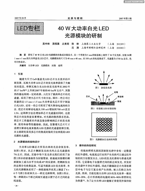
(40WLED电源 电路FAN6921.PDF)
- 格式:pdf
- 大小:154.11 KB
- 文档页数:1
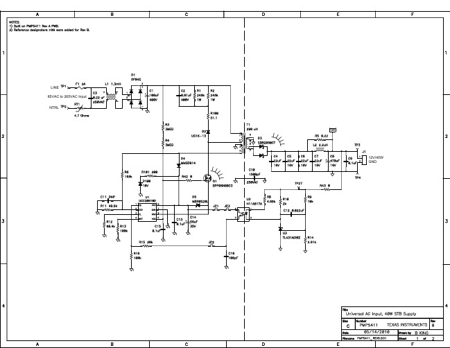
IMPORTANT NOTICE FOR TI REFERENCE DESIGNSTexas Instruments Incorporated("TI")reference designs are solely intended to assist designers(“Buyers”)who are developing systems that incorporate TI semiconductor products(also referred to herein as“components”).Buyer understands and agrees that Buyer remains responsible for using its independent analysis,evaluation and judgment in designing Buyer’s systems and products.TI reference designs have been created using standard laboratory conditions and engineering practices.TI has not conducted any testing other than that specifically described in the published documentation for a particular reference design.TI may make corrections,enhancements,improvements and other changes to its reference designs.Buyers are authorized to use TI reference designs with the TI component(s)identified in each particular reference design and to modify the reference design in the development of their end products.HOWEVER,NO OTHER LICENSE,EXPRESS OR IMPLIED,BY ESTOPPEL OR OTHERWISE TO ANY OTHER TI INTELLECTUAL PROPERTY RIGHT,AND NO LICENSE TO ANY THIRD PARTY TECHNOLOGY OR INTELLECTUAL PROPERTY RIGHT,IS GRANTED HEREIN,including but not limited to any patent right,copyright,mask work right, or other intellectual property right relating to any combination,machine,or process in which TI components or services are used. Information published by TI regarding third-party products or services does not constitute a license to use such products or services,or a warranty or endorsement e of such information may require a license from a third party under the patents or other intellectual property of the third party,or a license from TI under the patents or other intellectual property of TI.TI REFERENCE DESIGNS ARE PROVIDED"AS IS".TI MAKES NO WARRANTIES OR REPRESENTATIONS WITH REGARD TO THE REFERENCE DESIGNS OR USE OF THE REFERENCE DESIGNS,EXPRESS,IMPLIED OR STATUTORY,INCLUDING ACCURACY OR COMPLETENESS.TI DISCLAIMS ANY WARRANTY OF TITLE AND ANY IMPLIED WARRANTIES OF MERCHANTABILITY,FITNESS FOR A PARTICULAR PURPOSE,QUIET ENJOYMENT,QUIET POSSESSION,AND NON-INFRINGEMENT OF ANY THIRD PARTY INTELLECTUAL PROPERTY RIGHTS WITH REGARD TO TI REFERENCE DESIGNS OR USE THEREOF.TI SHALL NOT BE LIABLE FOR AND SHALL NOT DEFEND OR INDEMNIFY BUYERS AGAINST ANY THIRD PARTY INFRINGEMENT CLAIM THAT RELATES TO OR IS BASED ON A COMBINATION OF COMPONENTS PROVIDED IN A TI REFERENCE DESIGN.IN NO EVENT SHALL TI BE LIABLE FOR ANY ACTUAL,SPECIAL,INCIDENTAL,CONSEQUENTIAL OR INDIRECT DAMAGES,HOWEVER CAUSED,ON ANY THEORY OF LIABILITY AND WHETHER OR NOT TI HAS BEEN ADVISED OF THE POSSIBILITY OF SUCH DAMAGES,ARISING IN ANY WAY OUT OF TI REFERENCE DESIGNS OR BUYER’S USE OF TI REFERENCE DESIGNS.TI reserves the right to make corrections,enhancements,improvements and other changes to its semiconductor products and services per JESD46,latest issue,and to discontinue any product or service per JESD48,latest issue.Buyers should obtain the latest relevant information before placing orders and should verify that such information is current and complete.All semiconductor products are sold subject to TI’s terms and conditions of sale supplied at the time of order acknowledgment.TI warrants performance of its components to the specifications applicable at the time of sale,in accordance with the warranty in TI’s terms and conditions of sale of semiconductor products.Testing and other quality control techniques for TI components are used to the extent TI deems necessary to support this warranty.Except where mandated by applicable law,testing of all parameters of each component is not necessarily performed.TI assumes no liability for applications assistance or the design of Buyers’products.Buyers are responsible for their products and applications using TI components.To minimize the risks associated with Buyers’products and applications,Buyers should provide adequate design and operating safeguards.Reproduction of significant portions of TI information in TI data books,data sheets or reference designs is permissible only if reproduction is without alteration and is accompanied by all associated warranties,conditions,limitations,and notices.TI is not responsible or liable for such altered rmation of third parties may be subject to additional restrictions.Buyer acknowledges and agrees that it is solely responsible for compliance with all legal,regulatory and safety-related requirements concerning its products,and any use of TI components in its applications,notwithstanding any applications-related information or support that may be provided by TI.Buyer represents and agrees that it has all the necessary expertise to create and implement safeguards that anticipate dangerous failures,monitor failures and their consequences,lessen the likelihood of dangerous failures and take appropriate remedial actions.Buyer will fully indemnify TI and its representatives against any damages arising out of the use of any TI components in Buyer’s safety-critical applications.In some cases,TI components may be promoted specifically to facilitate safety-related applications.With such components,TI’s goal is to help enable customers to design and create their own end-product solutions that meet applicable functional safety standards and requirements.Nonetheless,such components are subject to these terms.No TI components are authorized for use in FDA Class III(or similar life-critical medical equipment)unless authorized officers of the parties have executed an agreement specifically governing such use.Only those TI components that TI has specifically designated as military grade or“enhanced plastic”are designed and intended for use in military/aerospace applications or environments.Buyer acknowledges and agrees that any military or aerospace use of TI components that have not been so designated is solely at Buyer's risk,and Buyer is solely responsible for compliance with all legal and regulatory requirements in connection with such use.TI has specifically designated certain components as meeting ISO/TS16949requirements,mainly for automotive use.In any case of use of non-designated products,TI will not be responsible for any failure to meet ISO/TS16949.Mailing Address:Texas Instruments,Post Office Box655303,Dallas,Texas75265Copyright©2013,Texas Instruments Incorporated。

l e d屏专用V A开关电源电原理图公司内部编号:(GOOD-TMMT-MMUT-UUPTY-UUYY-DTTI-l e d屏专用5V40A开关电源,用T L494、K A7500等集成块,通用设计TL494电路图的工作原理,主要是各元件的功能整流器之前的不用说了吧?494 脉宽调制输出至V3、V4。
494 的各脚功能请看其pdf资料。
1 脚是比较器+输入端,接电压监测。
如图,VR1 是输出电压调整。
V3、V4 是功率推动三极管。
T2是推动变压器,将推动电压提高以驱动末级功率管,末级工作在开关状态。
V2、V3 接成推挽功率放大。
VD5、VD6是反峰保护二极管。
R3、C8是尖峰吸收网络。
VD9、VD10、C9 组成全波整流滤波,给494供电。
T1 的右部分就是低压部分了。
整流滤波输出,没什么特别的。
220V交流电经VD1整流,C5,C6滤波得到300V左右直流电。
此电压经R1,R2分压后约150V给C7充电,经T1高压8,9脚绕组,T2绕组8,6脚,V2等形成启动电流。
T2反馈绕组7,9绕组,10,6绕组产生感应电压,使V1,V2轮流导通。
因此在T1低压供电绕组(6,7,13)产生电压,经VD9,VD10整流,C9滤波,给TL494,,V3,V4等供电。
此时输出电压较低。
TL494启动后其8脚,11脚轮流输出脉冲,推动V3,V4,经T2反馈给绕组(7.9,10.6)激励V1,V2。
使V1,V2,由自激状态转入受控状态。
T2输出绕组电压上升,此电压经R31,R29,R30,VR1分压后反馈给TL494的1脚(电压反馈)使输出电压稳定。
J1,J2是电流取样电阻,充电或输出时J1,J2产生压降。
此电压经R36反馈给TL494的15脚(电流反馈)使充电或输出电流恒定。
大体原理已经说清楚了,具体原理还有什么不明白追问,我就不一一说明每个元件的作用了。
R8,R9,R40 是V2的偏置电阻,VD8反馈整流,经R10,R11到V2基极,加速V2导通,C11是加速电容,可以加速V2的导通和截止。

ed节能灯电路图及制作过程ed节能灯电路图及制作过程为了让广大的电子爱好者和电子DIY发烧友能够自己制作简易的贴片LED节能灯,现博主特意为广大的朋友奉献一款贴片LED节能灯的制作资料和贴片LED灯的简易制作过程包含贴片LED节能灯制作电路图,以下是10贴片LED灯的制作电路图:图1是一款贴片LED照明灯具的实用电路图,该灯使用220V电源供电,220V交流电经C1降压电容降压后经全桥整流再通过C2滤波后经限流电阻R3给串联的10颗贴片LED提供恒流电源.贴片LED的额定电流为20mA,但是我们在制作节能灯的时候要考虑很多方面的因素对贴片LED的影响,包括光衰和发热的问题,LED的温度对光衰和寿命影响很大,如果散热不好很容易产生光衰,因为LED的特性是温度升高电流就会增大,所以一般在做大功率照明时散热的问题是最重要的,将影响到LED的稳定性,小功率一般都采取自散热方式,所以在电路设计时电流不宜过大.图中R1是保护电阻,R2是电容C1的卸放电阻,R3是限流电阻防止电压升高和温度升高LED的电流增大,C2是滤波电容,实际在LED电路中可以不用滤波电路,C2是用来防止开灯时的冲击电流对LED的损害,开灯的瞬间因为C1的存在会有一个很大的充电电流,该电流流过LED将会对LED产生损伤,有了C2的介入,开灯的充电电流完全被C2吸收起到了开灯防冲击保护.该电路是小功率灯杯最实用的电路,占用体积小可以方便的装在空间较小的灯杯里,现在被灯杯产品广泛的采用.优点:恒流源,电源功耗小,体积小,经济实用.但是在设计时降压电容要采用耐压在400V以上的涤纶电容或CBB电容,滤波电容要用耐压250v以上.此电路适合驱动7-12只20mA的贴片LED图2是电路板图PCB这中圆形的板子手工制作比较麻烦,建议买成品板。
以下给大家介绍制作全过程选择贴片LED贴片LED要选用高亮度的,产品亮度:5500-6000MCD(纯白光),电压:3.2-3.4V,电流:20MA,焊接温度:250发光角度:120色温:5500K。
夏普液晶电视46LX450电源板及背光电路详解是家电维修同行就会将您加进群或者长按二维码加群主微信夏普液晶电视46LX450电源板及背光电路祥解与实测数据该机的电源板分为待机电源产生电路芯片U7008,型号是A6059,PFC电路芯片U7010:型号是FAN7930,主开关电源芯片U7004,型号是L659,背光电路芯片U7201,型号是MP24830。
一、待机电源产生电路:主要由待机电源控制器U7008,开关电源变压器T7001组成。
上图中的C7025没有安装实物,空位。
输入电视机的220V市电,经D7031\D7032\D7033\D7034桥式整流,变成100HZ、310VP的全波脉动电压,形状像一个紧挨一个的馒头,为待机电源电路和PFC电路供电,注意桥式整流之后,并没有接大电解电容进行滤波,因为PFC电路的输入端输入的是馒头波,而不是经大电解电容滤波之后平滑的310V电压。
这是与老式CRT彩电开关电源桥式整流电路最显著的区别。
待机电源控制器U7008简介:芯片型号:A6059。
这是一个脉冲调宽型电流模式开关电源芯片,8脚双列直插封装。
该芯片集成了功率MOSFET和电流模式PWM控制器,低待机功率是通过PWM操作在轻负载条件下正常运行和突发振荡之间的自动切换.该芯片实现了高性价比的电源系统与极少的外部元件,内置的随机切换功能,可减少EMI噪声,实现了简化的(低成本)EMI滤波器,轻微的随机变化PMW频率fOSC,自动待机功能可以进入突发振荡模式,实现低待机功耗。
芯片内置启动电路,从而实现了低功耗。
芯片5脚内部设有VCC 欠压保护功能,在1脚内部设有过流保护功能。
引脚功能简介:1:S/OCP:内部MOS开关管的源极,且设有过流检测电路,当开关管过流时,停止开关电源的工作。
2:电网欠压检测输入端。
220V市电经桥式整流和D7022-----C7071的平滑滤波后,经串联电阻分压取样,加到2脚,用于监视220V市电的高低,当220V电网电压降低到150V以下时,会引起芯片内MOS开关管的过流而损坏,此时2脚检测到这一情况,关断本开关电源的工作,防止烧坏芯片。
AN983/DA Simplified Power Supply Design Using the TL494Control CircuitPrepared by: Jade H. Alberkrack ON Semiconductor Bipolar IC DivisionThis bulletin describes the operation and characteristics of the TL494 SWITCHMODE t V oltage Regulator and shows its application in a 400–watt off–line power supply.The TL494 is a fixed–frequency pulse width modulation control circuit, incorporating the primary building blocks required for the control of a switching power supply. (See Figure 1). An internal linear sawtooth oscillator is frequency–programmable by two external components, R T and C T . The oscillator frequency is determined by:f osc ^ 1.1R T @C TOutput pulse width modulation is accomplished by comparison of the positive sawtooth waveform across capacitor C T to either of two control signals. The NOR gates,which drive output transistors Q1 and Q2, are enabled only when the flip–flop clock–input line is in low state. Thishappens only during that portion of time when the sawtooth voltage is greater than the control signals. Therefore, an increase in control–signal amplitude causes a corresponding linear decrease of output pulse width. (Refer to the timing diagram shown in Figure 2).The control signals are external inputs that can be fed into the dead–time control (Figure 1, Pin 4), the error amplifier inputs (Pins 1, 2, 15, 16), or the feedback input (Pin 3). The dead–time control comparator has an effective 120 mV input offset which limits the minimum output dead time to approximately the first 4% of the sawtooth–cycle time. This would result in a maximum duty cycle of 96% with the output mode control (Pin 13) grounded, and 48% with it connected to the reference line. Additional dead time may be imposed on the output by setting the dead–time control input to a fixed voltage, ranging between 0 to 3.3 V .Figure 1. TL494 Block DiagramThis document may contain references to devices which are no longer offered. Please contact your ON Semiconductor representative for information on possible replacement devices.APPLICATION NOTEFigure 2. TL494 Timing DiagramCapacitor CFeedback/P The pulse width modulator comparator provides a means for the error amplifiers to adjust the output pulse width from the maximum percent on–time, established by the dead–time control input, down to zero, as the voltage at the feedback pin varies from 0.5 to 3.5 V . Both error amplifiers have a common mode input range from –0.3 V to (V CC –2V), and may be used to sense power supply output voltage and current. The error amplifier outputs are active high and are ORed together at the inverting input of the pulse width modulator comparator. With this configuration, the amplifier that demands minimum output on time, dominates control of the loop.When capacitor C T is discharged, a positive pulse is generated on the output of the dead–time comparator, which clocks the pulse steering flip–flop and inhibits the output transistors, Q1 and Q2. With the output mode control connected to the reference line, the pulse–steering flip–flop directs the modulated pulses to each of the two output transistors alternately for push–pull operation. The output frequency is equal to half that of the oscillator. Output drive can also be taken from Q1 or Q2, when single–ended operation with a maximum on–time of less than 50% is required. This is desirable when the output transformer has a ringback winding with a catch diode used for snubbing.When higher output drive currents are required for single–ended operation, Q1 and Q2 may be connected in parallel, and the output mode control pin must be tied to ground to disable the flip–flop. The output frequency will now be equal to that of the oscillator.The TL494 has an internal 5 V reference capable of sourcing up to 10 mA of load currents for external bias circuits. The reference has an internal accuracy of ±5% witha thermal drift of less than 50 mV over an operating temperature range of 0 to 70°C.APPLICATION OF THE TL494 IN A 400 OFF–LINE POWER SUPPLYA 5 V , 80 A line operated 25 kHz switching power supply,designed around the TL494, is shown in Figure 3, and the performance data is shown in Table 1. A brief explanation of each section of the power supply is as follows:AC Input SectionThe operating ac line voltage is selectable for nominal of 115 or 230 volts by moving the jumper links to their appropriate positions. The input circuit is a full wave voltage doubler when connected for 115 V AC operation with both halves of the bridge connected in parallel for added line–surge capability. When connected for 230 V AC operation, the input circuit forms a standard full wave bridge.The line voltage tolerance for proper operation is –10,+20% of nominal. The ac line inrush current, during power up, is limited by resistor R1. It is shorted out of the circuit by triac Q1, only after capacitors C1 and C2 are fully charged,and the high frequency output transformer T1, commences operation.Power SectionThe high frequency output transformer is driven in a half–bridge configuration by transistors Q3 and Q5. Each transistor is protected from inductive turn–off voltage transients by an R–C snubber and a fast recovery clamp rectifier. Transistors Q2 and Q4 provide turn–off drive to Q3and Q5, respectively. In order to describe the operation of Q2, consider that Q6 and Q3 are turned on. Energy iscoupled from the primary to the secondary of T3, forward biasing the base–emitter of Q3, and charging C3 through CR1. Resistor R3 provides a dc path for the ‘on’ drive after C3 is fully charged. Note that the emitter–base of Q2 is reverse biased during this time. Turn–off drive to Q3 commences during the dead–time period, when both Q6 and Q7 are off. During this time, capacitor C3 will forward bias the base–emitter of Q2 through R3 and R2 causing it to turn on. The base–emitter of Q3 will now be reverse biased by the charge stored in C3 coupled through the collector–emitter of Q2.Output SectionThe ac voltage present at the secondaries of T1 is rectified by four MBR 6035 Schottky devices connected in a full wave center tapped configuration. Each device is protected from excessive switching voltage spikes by an R–C snubber, and output current sharing is aided by having separate secondary windings. Output current limit protection is achieved by incorporating a current sense transformer T4. The out–of–phase secondary halves of T1 are cross connected through the core of T4, forming a 1–turn primary. The 50 kHz output is filtered by inductor L1, and capacitor C4. Resistor R4 is used to guarantee that the power supply will have a minimum output load current of 1 ampere. This prevents the output transistors Q3 and/or Q5 from cycle skipping, as the required on–time to maintain regulation into an open circuit load is less than that of the devices storage time. Transformer T5 is used to reduce output switching spikes by providing common mode noise rejection, and its use is optional.The MC3423, U1, is used to sense an overvoltage condition at the output, and will trigger the crowbar SCR, Q8. The trip voltage is centered at 6.4 V with a programmed delay of 40 m s. In the event that a fault condition has caused the crowbar to fire, a signal is sent to the control section via jumper ‘A’ or ‘B.’ This signal is needed to shut down the output, which will prevent the crowbar SCR from destruction due to over dissipation. Automatic over voltage reset is achieved by connecting jumper ‘A’. The control section will cycle the power supply output every 2 seconds until the fault has cleared. If jumper ‘B’ is connected, SCR Q12 will inhibit the output until the ac line is disconnected. Low Voltage Supply SectionA low current internal power supply is used to keep the control circuitry active and independent from external loading of the output section. Transformer T2, Q9 and CR2 form a simple 14.3 V series pass regulator.Control SectionThe TL494 provides the pulse width modulation control for the power supply. The minimum output dead–time is set to approximately 4% by grounding Pin 4 through R5. The soft start is controlled by C5 and R5. Transistor Q11 is used to discharge C5 and to inhibit the operation of the power supply if a low ac line voltage condition is sensed indirectly by Q10, or the output inhibit line is grounded.Error amplifier 1 and 2 are used for output voltage and current–level sensing, respectively. The inverting inputs of both amplifiers are connected together to a 2.5 V reference derived from Pin 14. By connecting the two inputs together, only one R–C feedback network is needed to set the voltage gain and roll off characteristics for both amplifiers. Remote output voltage sensing capability is provided, and the supply will compensate for a combined total of 0.5 V drop in the power busses to the load. The secondary of the output current sense transformer T4, is terminated into 36 W and peak detected by BR1 and C6. The current limit adjust is set for a maximum output current of 85 amperes.The oscillator frequency is set to 50 kHz by the timing components R T and C T. This results in a 25 kHz two phase output drive signal, when the output mode (Pin 13) is connected to the reference output (Pin 14).Table 1. 400 Watt Switcher Performance DataFigure 3. 400 Watt Switchmode Power SupplyTransformer DataT1Core:Bobbin:Windings:Ferroxcube EC 70–3C8, 0.002″ gap in each legFerroxcube 70PTBPrimary (Q3, Q5):Primary (Q1):Secondary, 4 each:Shield, 2 each:50 turns total, #17 AWG Split wound about secondary.4 turns, #17 AWG.3 turns, #14 AWG Quad Filar wound.Made from soft alloy copper 0.002″ thick.T2Core:Bobbin:Windings:Allegheny Ludlum EI–75–M6, 29 gaugeBobbin Cosmo EI 75Primary, 2 each:Secondary:1000 turns, #36 AWG.200 turns, #24 AWG.T3Core:Windings:Ferroxcube 846 T250–3C8Primary, 2 each:Secondary, 2 each:30 turns, #30 AWG Bifilar wound.12 turns, #20 AWG Bifilar wound.T4Core:Windings:Magnetics Inc. 55059–A2Primary, 2 each:Secondary:1 turn, #14 AWG Quad Filar wound. Taken from secondary to T1.500 turns, #30 AWG.T5Core:Windings:Magnetics Inc. 55071–A2Primary:Secondary:4 turns, #16 AWG Hex Filar wound.4 turns, #16 AWG Hex Filar wound.L1Core:Windings:TDK H7C2 DR 56 x 355 turns, soft alloy copper strap, 0.9″ wide x 0.020″ thick,6 m H.SWITCHMODE is a trademark of Semiconductor Components Industries, LLC.ON Semiconductor and are registered trademarks of Semiconductor Components Industries, LLC (SCILLC). SCILLC reserves the right to make changes without further notice to any products herein. SCILLC makes no warranty, representation or guarantee regarding the suitability of its products for any particular purpose, nor does SCILLC assume any liability arising out of the application or use of any product or circuit, and specifically disclaims any and all liability, including without limitation special, consequential or incidental damages. “Typical” parameters which may be provided in SCILLC data sheets and/or specifications can and do vary in different applications and actual performance may vary over time. All operating parameters, including “Typicals” must be validated for each customer application by customer’s technical experts. SCILLC does not convey any license under its patent rights nor the rights of others.SCILLC products are not designed, intended, or authorized for use as components in systems intended for surgical implant into the body, or other applications intended to support or sustain life, or for any other application in which the failure of the SCILLC product could create a situation where personal injury or death may occur. Should Buyer purchase or use SCILLC products for any such unintended or unauthorized application, Buyer shall indemnify and hold SCILLC and its officers, employees, subsidiaries, affiliates, and distributors harmless against all claims, costs, damages, and expenses, and reasonable attorney fees arising out of, directly or indirectly, any claim of personal injury or death associated with such unintended or unauthorized use, even if such claim alleges that SCILLC was negligent regarding the design or manufacture of the part. SCILLC is an Equal Opportunity/Affirmative Action Employer. PUBLICATION ORDERING INFORMATIONJAPAN: ON Semiconductor, Japan Customer Focus Center2–9–1 Kamimeguro, Meguro–ku, Tokyo, Japan 153–0051Phone: 81–3–5773–3850Email: r14525@。
摘自化学工业出版社出版的《液晶彩电电源板电路维修图集》(贺学金主编)一、TCL王牌液晶电视1. TCL王牌LCD3726电源方案电路图22. TCL PWL42C电源方案电路图33. TCL JSK3220晶辰电源方案电路图44. TCL ON37A电源方案电路图55. TCL PWL37C电源方案电路图66. TCL PWL3222电源方案电路图77. TCL PWL3235电源方案电路图88. TCL IPL42A/L电源方案电路图99. TCL IPL32L电源方案电路图1110.TCL PWL4201C电源方案电路图1411. TCL IPL22C电源方案电路图1712. TCL JSK4550-007ASCH电源板电路图1813. TCL LC32L6-PWO(晶辰)电源电路图1914. TCL LCD20B66电源电路图2015. TCL JSK4338-007A电源板电路图2116. LPL32S电源方案电路图22二、长虹液晶电视1. 长虹LT26510电源电路图262.长虹FSP038-2L01电源电路图273. 长虹FSP090-3PS01电源电路图284. 长虹FSP090L-3HF01电源电路图305. 长虹FSP107-2PS01电源电路图326. 长虹FSP107-2PS03电源电路图347. 长虹FSP107P-3HF04电源电路图368. 长虹FSP140-3PS01电源电路图389. 长虹FSP140-3PS02电源电路图4010. 长虹FSP150-3PS01电源电路图4211. 长虹FSP150P-3HF02电源电路图4412. 长虹FSP160-3PI01电源电路图4613. 长虹FSP196P-3HF01电源电路图4814. 长虹FSP236-3PS01电源电路图5015. 长虹FSP250-3PI03电源电路图52116. 长虹FSP270-3PI05电源电路图5417. 长虹FSP304-3PI01电源电路图5618. 长虹HS080L-2HF01电源电路图5819. 长虹HS140P-3HF01电源电路图6020. 长虹R-HS180P-3HF01电源电路图6221.长虹R-HS368-4N01电源电路6422. 长虹FSP242-4F01电源电路图66三、创维液晶电视1. 创维JSK3250开关电源电路图682. 创维52英寸液晶电视电源电路图693. 创维LED液晶电视169P-P32ELU-00电源电路图704. 创维37英寸液晶电视电源电路图715. 创维P32TQF-0000电源电路图726. 创维168P-P47TTS-00电源电路图737. 创维168P-P46TTS-02电源电路图748. 创维168P-P32TTS-21电源电路原理图759. 创维3L05HR2电源电路图7610. 创维24E61HR型LED液晶电视电源电路图7711. 创维P37-TTS-37L01HM电源电路图7812. 创维8H01电源电路图8013. 创维19英寸液晶电视电源电路图8114. 创维26英寸液晶电视二合一电源电路图8215. 创维32L05HR电源电路图8316. 创维5800-P32TTU-0150电源电路图8517. 创维P32TLF电源电路图8618. 创维P26TQI电源电路图8719. 创维37TTF电源电路图8820. 创维168P-P47TTP-00电源电路图8921. 创维168P-P32TTF电源电路图9022. 创维55英寸LED液晶电视电源电路图91四、海信液晶电视1.海信LED液晶电视2031电源板电路图982.海信RAG7.820.848A电源板电路图1013. 海信TLM3277型电路图1034. 海信TLM42V89PKV(0011)系列(2169板)电源电路图1045. 海信TLM37V68(5)系列(1731板)电源电路图1056. 海信超薄液晶TLM42T69GP系列(1535板)电源电路图1067. 海信TLM42V86PKV(4)系列(2123板)电源电路图1078. 海信RSAG7. 850. 568A_TLM477电源电路图1099. 海信RSAG7. 820. 1235_TLM2633D_TLM26E29电源电路图11010. 海信TLM37V66K系列(1768板)电源电路图11111. 海信TLM46V66PK系列(2184板)电源电路图112212. 海信TLM47V88PK系列(2309板)电源电路图11313. 海信TLM52V78PKN系列(2100板)电源电路图11414. 海信TLM19V68系列(1585板)电源电路图11515. 海信TLM22V68(3)系列(1569板)电源电路图11616. 海信TLM26V68(1)系列(1646板)电源电路图11717. 海信TLM32V88PK(1)系列(1666板)电源电路图11818. 海信TLM40V68PK(3)系列(1901板)电源电路图11919. 海信TLM40V69P系列(RSAG7. 820. 1374板)电源电路图12020. 海信26英寸LED液晶电视开关电源电路图12121. 海信TLM40V68P(2)系列(1673板)电源电路图12322. 海信TLM3233H系列(1032板)电源电路图124五、康佳液晶电视1. 康佳KPS180-01电源电路图1262. 康佳KPS180-02电源电路图1283. 康佳KPS270-01电源电路图1304. 康佳KPS300-01电源电路图1335. 康佳KPS430-01电源电路图1356. 康佳KPS+L036C1-01电源电路图1387. 康佳超薄型KPS+L180C3-01电源电路图1398. 康佳KPS+L200C3-01电源电路图1419. 康佳KPS+L310C3-01电源电路图14310. 康佳KIP036I02-01电源电路图14511. 康佳KIP048I04-01电源电路图14712. 康佳KIP060I04-01电源电路图14913. 康佳KIP072I12-01电源电路图15114. 康佳KIP072U04-01电源电路图15315. 康佳KIP150I12-01电源电路图15516. 康佳KIP150U04-01电源电路图15817. 康佳KIP220I16-01电源电路图16218. 康佳KIP+L048U02C1-01电源电路图16419. 康佳KIP+L100U04C1-01电源电路图16620. 康佳KIP+L150I12C1-01电源电路图17021. 康佳KIP+L150I14C1-01电源电路图17322. 康佳KIP+L180C3-02电源电路图17623. 康佳KIP+L200I12C1-01电源电路图17824. 康佳LC32AS28(台达)电源电路图18225. 康佳LC-TM3719电源电路图183六、其他品牌液晶电视1. 厦华T号电源电路图1862. 厦华U号电源电路图1873. 厦华R号电源电路图1884. 厦华37HU型电源电路图18935. 海尔H32E07型电源电路图1906. LG STR-W6853P电源方案电路图1917. LG 19LG3000型电源电路图1928. 冠捷(AOC)L427A31型电源电路《液晶电视电源电路维修图集》(贺学金主编)特点是:精选了创维、TCL、康佳、海信、长虹、厦华、海尔、LG等液晶彩电一百多种电源电路,基本涵盖了当前主流液晶电视电源的电路类型。
LED手电制作电路及充电器电路图LED手电制作电路时间:2007-08-27 来源: 作者: 点击:15730 字体大小:【大中小】LED手电具有省电、耐用、亮度强等优点。
非常受欢迎,这里介绍一个LED手电制作的经典电路,供大家参考。
1、1.5V低成本LED驱动电路磁环选用T9*5*3/2K,也可用T10*6*5等,用0.3mm漆包线双线并绕20T,按图中同名端连接。
TR1选8050或9014,D1选4937或107,PCB用一片废板自制。
2、1.2v升3.4v电源电路利用单晶体管构建智能的电池充电器电路图本文的自动电池充电器电路设计采用了一种电路,该电路可以称得上有史以来用单个晶体管制造的最简单的窗口比较器(见图)。
当电压下降到预定值以下时它开始充电,当电压超过预定值时它停止充电。
借助精确的可变电压电源,可在设定上下电压。
正常连接的继电器引线不接入15V dc电源,它阻止了电压传至电池引线。
这样可以精确设置上下电压。
但15 V dc的充电电源被连接至电路。
首先,可变电压电源被固定在13.3 V dc——这是电池充满电的电压,并被连接至电路的电池连接点。
VR1的滑块被调到附在电池正极的最顶端。
VR2的滑块应向连接至VR1的一端调节。
该晶体管开始工作,分流VR1。
然后,VR1的滑块向另一端调节,即连接至VR2的一端。
现在将测试电源电压设为11.8 V dc,这是电池耗尽时的电压。
然后,调节VR2以使它让晶体管不再工作。
测试电压再提高至13.3 V dc,调节VR1使晶体管工作。
利用设置的上下电压,NC点被连接至电路(15V dc充电电压)。
现在电池充电器已经就绪了。
典型半桥式电动自行车电瓶充电器电路图下图是天能TN-1智能负脉冲充电器电路图。
这个充电器主要部分是典型的半桥式两段充电器。
这里主要介绍负脉冲充电部分的工作原理。
这部分电路由放电开关、负脉冲加载控制、脉冲振荡器三部分组成。
放电开关是三极管Q6、Q6导通,其集电极和发射极将电瓶短路,电瓶放电。