TLP222A_07中文资料
- 格式:pdf
- 大小:191.63 KB
- 文档页数:6
Forward current IF (mA)
100 Ta = 25°C
30
10
IF – VF
3 1
0.3
0.1
0.6
0.8
1
1.2
1.4
1.6
1.8
Forward voltage VF (V)
On-state current ION (mA)
600 Ta = 25°C
IF = 5 mA 400
ION – VON
Isolation voltage
Symbol CS RS
BVS
Test Condition
VS = 0 V, f = 1 MHz VS = 500 V, R.H. <= 60% AC, 1 min AC, 1 s, in oil DC, 1 min, in oil
TLP222A,TLP222A-2
Min Typ. Max Unit
⎯
1.6
3
mA
0.1
⎯
⎯
mA
⎯
1
2
Ω
Min Typ. Max Unit
⎯
0.8
⎯
pF
5 × 10¹⁰ 1014
⎯
Ω
2500 ⎯
⎯
Vrms
⎯ 5000 ⎯
⎯ 5000 ⎯ Vdc
Switching Characteristics (Ta = 25°C)
Characteristics Turn-on time Turn-off time
IF ΔIF/°C
IFP VR Tj VOFF
ION
ΔION/°C
Tj Tstg Topr Tsol BVS
50
mA
−0.5
mA/°C
1
A
5
V
125
°C
60
V
500
mA
−5.0
mA/°C
125 −55 to 125 −40 to 85
260
2500
°C °C °C °C
Vrms
Note: Using continuously under heavy loads (e.g. the application of high temperature/current/voltage and the significant change in temperature, etc.) may cause this product to decrease in the reliability significantly even if the operating conditions (i.e. operating temperature/current/voltage, etc.) are within the absolute maximum ratings. Please design the appropriate reliability upon reviewing the Toshiba Semiconductor Reliability Handbook (“Handling Precautions”/“Derating Concept and Methods”) and individual reliability data (i.e. reliability test report and estimated failure rate, etc).
TLP222A-2
One channel operation
Two channel operations
Junction temperature
Storage temperature
Operating temperature
Lead soldering temperature (10 s)
Isolation voltage (AC, 1 min, R.H. <= 60%) (Note 1)
Note 1: LED pins are shorted together. Detector pins are also shorted together.
Recommended Operating Conditions
Characteristics
Symbol
Min Typ. Max Unit
Supply voltage Forward current On-state current Operating temperature
JEDEC
―
JEITA
―
TOSHIBA
11-5B2
Weight: 0.26 g (typ.)
TLP222A-2
JEDEC
―
JEITA
―
TOSHIBA
11-10C4
Weight: 0.54 g (typ.)
1
2007-10-01
元器件交易网
TLP222A,TLP222A-2
5
ION = 500 mA t<1s 4
IFT – Ta
3
2
1
0
−20
0
20
40
60
80
100
Ambient temperature Ta (°C)
4
2007-10-01
On-state resistance RON (Ω)
元器件交易网
Switching time tON, tOFF (μs)
4
RL
VOUT 3
IF VOUT
10% tON
90% tOFF
IF 1
TLP222A-2
VDD
8
RL
VOUT
2
7
3
2007-10-01
元器件交易网
Allowable forward current IF (mA)
IF – Ta
100
80
60
40
20
0
−20
0
20
40
60
Junction temperature
Off-state output terminal voltage
TLP222A
On-state current
Detector
TLP222A-2
One channel operation
Two channel operations
TLP222A
Forward current derating (Ta >= 25°C)
80 100 120
Ambient temperature Ta (C)
On-sate current ION (mA)
TLP222A,TLP222A-2
ION – Ta
600
500
400
300
200
100
0
−20
0
20
40
60
80 100 120
Ambient temperature Ta (°C)
0.3
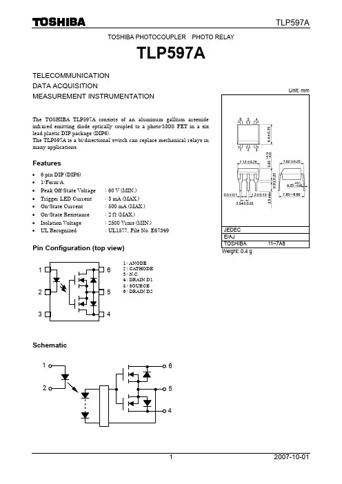
Pin Configuration (top view)
TLP222A
TLP222A-2
1
4
1
8
2
1: Anode 2: Cathode 3: Drain 4: Drain
2
7
3
3
6
4
5
1, 3 : Anode 2, 4 : Cathode 5 : Drain D1 6 : Drain D2 7 : Drain D3 8 : Drain D4
Absolute Maximum Rating (Ta = 25°C)
Characteristics
Symbol
Rating
Unit
Forward current Forward current derating (Ta >= 25°C) LED Peak forward current
Reverse voltage
Note 2: Switching time test circuit
Symbol
Test Condition
Min Typ. Max Unit
tON tOFF
RL = 200 Ω VDD = 20 V, IF = 5 mA
⎯ (Note 2) ⎯
0.8
2
ms
0.1 0.5
IF 1
TLP222A
2
VDD
Unit: mm TLP222A
The Toshiba TLP222A and TLP222A-2 consist of a gallium arsenide infrared emitting diode optically coupled to a photo-MOSFET in a DIP package whose withstanding voltage is 60 V. These photorelays have higher output current rating than phototransistor-type photocoupler; hence, they are suitable for use as On/Off control for high current.
元器件交易网 TLP222A,TLP222A-2
TOSHIBA Photocoupler Photorelay
TLP222A, TLP222A-2
Telecommunications Measurement and Control Equipment Data Acquisition System Measurement Equipment