
12PA5-BK;12PA5-W;中文规格书,Datasheet资料
- 格式:pdf
- 大小:39.32 KB
- 文档页数:2


Special Use Sensors - Weldable Strain GagesStandard Weldable PatternsMicro-Measurements For technical questions, contact: micro-measurements@Document Number: 11519Micro-Measurements Standard Weldable Strain Gages and Temperature Sensors are specially designed for spot welding to structures and components. They are ideal for applications where test or environmental conditions preclude clamping and curing an adhesively bonded gage installation.These gages are equally advantageous when strain measurements must be made at an elevated temperature,but the nature of the test object does not permit the use of an elevated-temperature-curing adhesive.Surface preparation requirements are minimal; only an appropriate solvent cleaning and abrasion of the test part surface with silicon-carbide paper or a small, hand-held grinder is needed. Spot welding is accomplished with a portable stored-energy hand-probe spot welder, such as the Model 700. Environmental protection is as easily applied to a welded gage installation as to an adhesively bonded gage.Refer to Instruction Bulletin B-131 and Catalog A-110 for further information on installation and protective coatings,and to Bulletin 302 for specifications on the Model 700Welding/Soldering Unit.DESCRIPTION AND PERFORMANCEGeneral — All sensors are laboratory-prebonded, with a high-performance adhesive, to thin (0.005 in [0.13 mm])metal carriers. Sensor grids are fully encapsulated for protection against handling and installation damage.Standard weldable strain gages are offered in two series to meet differing performance requirements. Both series are available in either 06 or 09 self-temperature compensation.Strain gages with 06 S-T-C have Inconel carriers, while S-T-C 09 gages and temperature sensors are mounted on 300-series stainless steel.CEA-Series Welda le Strain Gage —Polyimide-encapsulated constantan foil grid, with large, rugged,copper-coated tabs. In most cases, the carrier can be contoured to a radius as small as 1/2in [13mm]. The CEASeries is ideal for direct leadwire attachment, before or after installation.Strain range is ±5000µin/in [±5000µm/m], and normal operating temperature range is –100° to +200°F [–75° to +95°C]. Short-term maximum temperature is +300°F [+150°C].LWK-Series Weldab le Strain Gage — Nickel-chromium alloy grid, encapsulated in fiberglass-reinforced epoxy phenolic. The LWK gage is provided with a three-wire lead system with 10 in [250 mm] of Teflon ®-insulated leadwire.This construction simplifies leadwire temperature compensation and provides for easy connection of the lead system to the instrumentation cable. Minimum installation radius is generally limited to 2in [50 mm].Strain range is ±5000µin/in [±5000µm/m], and normal operating temperature range is –320° to +500°F [–195° to +260°C]. Short-term maximum temperature is +550°F [+290°C].WWT-Series Temperature Sensor — High-purity nickel foil grid encapsulated in fiberglass-reinforced epoxy-phenolic,and equipped with integral three-tab terminal to facilitate leadwire attachment. The temperature sensor is normally installed on a flat surface of the workpiece, but, in any case,should always be oriented with the gridlines in the direction of minimum strain to avoid strain-induced errors (see Micro-Measurements Tech Note TN-506, Bondable Resistance Temperature Sensors and Associated Circuitry).With an appropriate LST Matching Network, the temperature response characteristic of the nickel can be linearized and scaled for direct readout (in degrees) with any strain indicator.Teflon is a Registered Trademark of DuPont.MEASUREMENT CONSIDERATIONSIt is important to note that operating characteristics of weldable strain gages (gage factor, transverse sensitivity,and thermal output) are specified for the basic strain gage itself — without the metal carrier. Thus, the properties are measured by bonding a conventional strain gage directly to an appropriate calibration specimen, following standard methods specified for all Micro-Measurements strain gages. This procedure assures the most accurate results,independent of the variables introduced by welding. In particular, the user should be aware that the gage factor specified on the engineering data sheet accompanying the gage applies only to the basic strain gage, without the shim. The effective gage factor of the weldable assembly (after welding to the test member) is commonly 5 to 10%lower than this, due primarily to the stiffness of the shim.The reduction in gage factor is not subject to quantitative generalization, because it depends on the cross-sectional properties of the test specimen, and on the mode of loading (e.g., bending versus direct stress). It has been demonstrated, however, that for a group of like specimens, loaded in the same manner, the weldable gages exhibit very good repeatability and uniformity of response. Therefore, when test requirements dictate greatest accuracy, the weldable gages should be calibrated on a specimen of the same material and cross section as the test part, and under the same mode of loading.Special Use Sensors - Weldable Strain GagesStandard Weldable PatternsMicro-MeasurementsDocument Number: 11519For technical questions, contact: micro-measurements@Note 1: Products with designations and options shown in bold are not RoHS compliant.GAGE PATTERN AND DESIGNATIONInsert Desired S-T-C No. in Spaces Marked XX.See Note 1RES.IN OHMS.DIMENSIONSCARRIERACTIVE GRID MATRIX Length Width Thick Length Width Length Width CEA-XX-W250A-120CEA-XX-W250A-350120 ± 0.4%350 ± 0.4%0.630.340.0050.2300.1250.440.1716.08.60.135.843.1811.24.3Most flexible and conformable pattern. T ype 326-DFV and 330-DFV flat three-conductor cable typically used to solder directly to copper-coated tabs.CEA-XX-W250C-120CEA-XX-W250C-350120 ± 0.4%350 ± 0.4%0.900.900.0050.2300.1250.440.1722.922.90.135.843.1811.24.3Tee rosette, used in biaxial stress states where directions of principal stresses are known. See W250A pattern for typical leadwire recom-mendations.LWK-XX-W250B-350350 ± 0.4%0.880.320.0050.2500.1250.620.1722.48.10.136.353.1815.74.3Wide-temperature-range linear pattern with 10 in [250 mm] pre-attached leads. Teflon insulation is pretreated for best bond to protective coatings.LWK-XX-W250D-350350 ± 0.4%1.15 1.150.0050.2500.1250.620.1729.229.20.136.353.1815.74.3Tee rosette, used in biaxial stress states where directions of principal stresses are known and a wide operating temperature range is required.WWT -TG-W200B-05050 ± 0.4% @ +75°F [+24°C]0.710.430.0050.2000.2000.520.2618.010.90.135.085.0813.16.6Easy-to-use temperature sensor that can be welded or adhesively bonded to the test structure. For standard bondable temperature sensors, see Document Number 11522, “T emperature Sensors and LST Networks.”Vishay Precision GroupDisclaimerALL PRODUCTS, PRODUCT SPECIFICATIONS AND DATA ARE SUBJECT TO CHANGE WITHOUT NOTICE.Vishay Precision Group, Inc., its affiliates, agents, and employees, and all persons acting on its or their behalf (collectively, “Vishay Precision Group”), disclaim any and all liability for any errors, inaccuracies or incompleteness contained herein or in any other disclosure relating to any product.The product specifications do not expand or otherwise modify Vishay Precision Group’s terms and conditions of purchase, including but not limited to, the warranty expressed therein.Vishay Precision Group makes no warranty, representation or guarantee other than as set forth in the terms and conditions of purchase. To the maximum extent permitted by applicable law, Vishay Precision Group disclaims (i) any and all liability arising out of the application or use of any product, (ii) any and all liability, including without limitation special, consequential or incidental damages, and (iii) any and all implied warranties, including warranties of fitness for particular purpose, non-infringement and merchantability.Information provided in datasheets and/or specifications may vary from actual results in different applications and performance may vary over time. Statements regarding the suitability of products for certain types of applications are based on Vishay Precision Group’s knowledge of typical requirements that are often placed on Vishay Precision Group products. It is the customer’s responsibility to validate that a particular product with the properties described in the product specification is suitable for use in a particular application.No license, express, implied, or otherwise, to any intellectual property rights is granted by this document, or by any conduct of Vishay Precision Group.The products shown herein are not designed for use in life-saving or life-sustaining applications unless otherwise expressly indicated. Customers using or selling Vishay Precision Group products not expressly indicated for use in such applications do so entirely at their own risk and agree to fully indemnify Vishay Precision Group for any damages arising or resulting from such use or sale. Please contact authorized Vishay Precision Group personnel to obtain written terms and conditions regarding products designed for such applications.Product names and markings noted herein may be trademarks of their respective owners.分销商库存信息: VISHAYLWK-06-W250B-350。
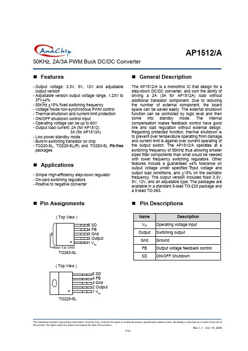
AP1512/A50KHz, 2A/3A PWM Buck DC/DC ConverterFeatures- Output voltage: 3.3V, 5V, 12V and adjustable output version- Adjustable version output voltage range, 1.23V to 37V+4%- 50KHz +15% fixed switching frequency- Voltage mode non-synchronous PWM control - Thermal-shutdown and current-limit protection - ON/OFF shutdown control input - Operating voltage can be up to 60V - Output load current: 2A (for AP1512)3A (for AP1512A)- Low power standby mode- Built-in switching transistor on chip - TO220-5L, TO220-5L(R) and TO263-5L Pb-free packagesApplications- Simple High-efficiency step-down regulator - On-card switching regulators - Positive to negative converterGeneral DescriptionThe AP1512/A is a monolithic IC that design for a step-down DC/DC converter, and own the ability of driving a 2A (3A for AP1512A) load without additional transistor component. Due to reducing the number of external component, the board space can be saved easily. The external shutdown function can be controlled by logic level and then come into standby mode. The internal compensation makes feedback control have good line and load regulation without external design. Regarding protected function, thermal shutdown is to prevent over temperature operating from damage, and current limit is against over current operating of the output switch. The AP1512/A operates at a switching frequency of 50KHz thus allowing smaller sized filter components than what would be needed with lower frequency switching regulators. Other features include a guaranteed +4% tolerance on output voltage under specified input voltage and output load conditions, and +15% on the oscillator frequency. The output version included fixed 3.3V, 5V, 12V, and an adjustable type. The packages are available in a standard 5-lead TO-220 package and a 5-lead TO-263.Pin AssignmentsTO220-5L( Top View )( Top View )TO263-5L INMetal Tab GNDINPin DescriptionsNameDescriptionV IN Operating voltage input Output Switching output Gnd Ground FBOutput voltage feedback controlSD ON/OFF ShutdownAP1512/A50KHz, 2A/3A PWM Buck DC/DC ConverterOrdering InformationPackage T5: TO220-5LK5: TO263-5LOutput Version AP1512 X XX X XPacking Blank : Tube A : TapingBlank : Adjustable -33 : 3.3V -50 : 5.0V -12 : 12VT5R: TO220-5L(R)Part Number Blank: 2A A : 3ABlock DiagramCurrent Source bias1.235V Reference2.5V Regulator50KHz OSC.Start up++_+_Thermal LimitPre-driverComp CompGndOutput V INSDFB220mV200mV2A Switch +__Amp CompFrequecy compen-sation(3A for AP1512A)AP1512/A50KHz, 2A/3A PWM Buck DC/DC ConverterAbsolute Maximum RatingsSymbol Parameter RatingUnit V CC Supply Voltage +63 V V SD ON/OFF Pin input voltage -0.3 to +40 V V FB Feedback Pin voltage -0.3 to +40V V OUT Output voltage to Ground -1V P D Power dissipation Internally limited W T ST Storage temperature -65 to +150 o C T OP Operating temperature -40 to +125 o C V OP Operating voltage+4.5 to +60VElectrical Characteristics (All Output Voltage Versions)Unless otherwise specified, V IN =30V for all version. I LOAD = 0.5ASymbol ParameterConditionsMin.Typ.Max. Unit 8I BFeedback bias currentV FB =1.3V(Adjustable version only)5 10µA42.5 50 57.5F OSC oscillator frequency40 60KHz1.4V SAT saturation voltage I OUT =2A no outside circuitV FB =0V force driver on1.3 1.5VMax. Duty Cycle(ON) V FB =0V force driver on100DCMin. Duty cycle(OFF) V FB =12V force driver off%4.5I CL current limit for AP1512 peak currentno outside circuitV FB =0V force driver on 2.5 3 5.5A5I CL current limit for AP1512A peak current no outside circuitV FB =0V force driver on3.2 4 6 A Output = 0no outside circuitV FB =12V force driver off-250 uA I L Output = -1 Output leakage currentV IN =60V -2 -60 mA I Q Quiescent Current V FB =12V force driver off 5 10 mA450 I STBYStandby Quiescent Current ON/OFF pin=5VV IN =60V 350 500uA V IL Low (regulator ON) - 0.6 V IH ON/OFF pin logic inputthreshold voltage High (regulator OFF) 2.0 1.3 - VI H ON/OFF pin logic input currentV LOGIC =2.5V (OFF) 0 -5I L ON/OFF pin input current V LOGIC =0.5V (ON) -0.8 -10uA TO220-5L 2.5 θJC Thermal Resistance TO263-5L Junction to case3.5 oC/WTO220-5L 28 θJA Thermal ResistanceWith copper area ofapproximately 3 in 2TO263-5L Junction to ambient 23 oC/WAP1512/A50KHz, 2A/3A PWM Buck DC/DC ConverterElectrical Characteristics (Continued)AP1512Symbol Parameter Conditions Typ. Limit Unit AP1512-ADJ FB V Output Feedback 10V < V IN < 60V 0.2A < I LOAD < 2AV OUT programmed for 3V 1.231.193/1.18 1.267/1.28 V V MIN V MAX AP1512-3.3V OUT V Output voltage 10V < V IN < 60V 0.2A < I LOAD < 2A 3.3 3.168/3.135 3.432/3.465 V V MIN V MAX AP1512-5VOUT V Output voltage 10V < V IN < 60V 0.2A < I LOAD < 2A 5 4.8/4.75 5.2/5.25 V V MIN V MAX OUT V Output voltage15V < V IN < 60V 0.2A < I LOAD < 2A12 11.52/11.4 12.48/12.6V V MIN V MAX AP1512-12VηEfficiency V IN = 30V, I LOAD = 2A 83 % AP1512ASymbol Parameter Conditions Typ. Limit Unit AP1512A-ADJ FB V Output Feedback 10V < V IN < 60V 0.2A < I LOADV OUT programmed for 3V 1.231.193/1.18 1.267/1.28 V V MIN V MAX AP1512A-3.3V OUT V Output voltage 10V < V IN < 60V 0.2A < I LOAD 3.3 3.168/3.135 3.432/3.465 V V MIN V MAX AP1512A-5VOUT VOutput voltage10V < V IN < 60V 0.2A < I LOAD54.8/4.755.2/5.25V V MIN V MAX OUT V Output voltage15V < V IN < 60V 0.2A < I LOAD12 11.52/11.4 12.48/12.6V V MIN V MAX AP1512A-12VηEfficiency V IN = 30V, I LOAD = 3A80%Specifications with boldface type are for full operating temperature range, the other type are for T J =25ºC.Typical Performance CharacteristicsAP1512A Current Limit v.s. Temperature(Vcc=60V, Vout=5V)33.23.43.63.84-50050100150Temperature (TA) (°C)C u r r e n t L i m i t (A )AP1512A Efficiency v.s. Supply Voltage(Vout=5V, Iout=3A)10203040506070809010001224364860Supply Voltage(V)E f f i c i e n c y (%)AP1512/A50KHz, 2A/3A PWM Buck DC/DC ConverterTypical Performance Characteristics (Continued)AP1512 Efficiency v.s. Temperature(Vin=12V,Vout=5V,Io=2A)102030405060708090100-50-30-101030507090*********Temperature (TA) (°C)E f f i c i e n c y (%)AP1512 Efficiency v.s. Temperature(Vin=12V,Vout=3.3V,Io=2A)102030405060708090100-50-30-101030507090*********Temperature (TA) (°C)E f f i c i e n c y (%)AP1512 Supply Current v.s. Temperature(Vcc=12V , No Load ,Von/off =0V(Switch ON) ,Von/off =5V(Switch OFF))12345678-40-25-105203550658095110125S u p p l y C u r r e n t (m A )Temperature (TA) (°C)Switch ON102030405060708090100-40-25-105203550658095110125S u p p l y C u r r e n t (u A )Temperature (TA) (°C)Switch OFFAP1512 Output Voltage v.s. Temperature(Vin=12V, Vout=5V, Io=1A)4.704.754.804.854.904.955.005.055.10-50050100150O u t p u t V o l t a g e (V )Temperature (TA) (°C)AP1512 Threshold Voltage v.s. Temperature(Vcc=12V, Vout=5V)00.20.40.60.811.21.41.6-50050100150T h r e s h o l d V o l t a g e (V )Temperature (TA) (°C)AP1512/A50KHz, 2A/3A PWM Buck DC/DC ConverterTypical Performance Characteristics (Continued)AP1512 Frequency v.s. Temperature(Vcc=12V, Io=1A, Vout=5V)4045505560-50-30-101030507090110130150Temperature (TA) (°C)F r e q u e n c y (K H z )AP1512 Current Limit v.s. Temperature(Vcc=60V, Vout=5V)2.833.23.43.6-5050100150C u r r e n t L i m i t (A )Temperature (TA) (°AP1512 Quiescent Current v.s. Supply Voltage(force driver off)5.25.45.65.866.21224364860Q u i e s c e n t C u r r e n t (A )Supply Voltage(V)AP1512/A50KHz, 2A/3A PWM Buck DC/DC ConverterTypical Application Circuit(1) Adjustable Type CircuitA. Vin=10V~60V, Vout=5V; Iout=0.3A~2A, Iout below 0.3A DCMC51nL147uH12R23KVinC21uD1SR360ON/OFFR31KC1100uF/100VAP1512/A15243VinSDOUTPUTFBGND 0.1uC3470uF/16VC7B. Vin=10V~60V, Vout=3.3V, Iout=0.3A~2A, Iout below 0.3A DCMC51nL147uH12R22KVinC21uD1SR360ON/OFFR31.2KC1100uF/100VAP1512/A15243VinSDOUTPUTFBGND 0.1uC3470uF/16VC7(2) Fixed Type CircuitA. Vin=10V~60V, Vout=5V, Iout=0.7A~2A, Iout below 0.7A DCML147uH12VinC21uD1SR360ON/OFFC1100uF/100VVoutAP1512/A15243VinSDOUTPUTFBGND 10nC3470uF/16VC7AP1512/A50KHz, 2A/3A PWM Buck DC/DC ConverterTypical Application Circuit (Continued)B. Vin=10V~60V, Vout=3.3V, Iout=0.7A~2A, Iout below 0.7A DCML133uH12VinC23.3uD1SR360ON/OFFC1220uF/100VVoutAP1512/A15243VinSDOUTPUTFBGND 3.3uC31500uF/16VC7Function Description+V INThis is the positive input supply for the IC switching regulator. A suitable input bypass capacitor must be present at this pin to minimize voltage transients and to supply the switching currents needed by the regulator.GroundCircuit ground.OutputInternal switch. The voltage at this pin switches between (+V IN – V SAT ) and approximately – 0.5V, with a duty cycle of approximately V OUT / V IN . To minimize coupling to sensitive circuitry, the PC board copper area connected to this pin should be kept a minimum.FeedbackSenses the regulated output voltage to complete the feedback loop.ON /OFFAllows the switching regulator circuit to be shutdown using logic level signals thus dropping the total input supply current to approximately 150uA. Pulling this pin below a threshold voltage of approximately 1.3V turns the regulator on, and pulling this pin above 1.3V (up to a maximum of 40V) shuts the regulator down. If this shutdown feature is not needed, the SD pin can be wired to the ground pin or it can be left open, in either case the regulator will be in the ON condition.Thermal ConsiderationsThe AP1512/A is available in two packages, a 5-pin TO-220 and a 5-pin surface mount TO-263.The TO-220 package needs a heat sink under most conditions. The size of the heatsink depends on the input voltage, the output voltage, the load current and the ambient temperature. The AP1512/A junction temperature rises above ambient temperature for a 2A load and different input and output voltages. The data for these curves was taken with the AP1512/A (TO-220 package) operating as a buckswitching regulator in an ambient temperature of 25o C (still air). These temperature rise numbers are all approximate and there are many factors that can affect these temperatures. Higher ambient temperatures require more heat sinking.The TO-263 surface mount package tab is designed to be soldered to the copper on a printed circuit board. The copper and the board are the heat sink for this package and the other heat producing components, such as the catch diode and inductor. The PC board copper area that the package is soldered to should be at least 0.4 in 2, and ideally should have 2 or more square inches of 2 oz. Additional copper area improves the thermal characteristics, but with copper areas greater than approximately 6 in 2, only small improvements in heat dissipation are realized. If further thermal improvements are needed, double sided, multilayer PC board with large copper areas and/or airflow are recommended.AP1512/A50KHz, 2A/3A PWM Buck DC/DC ConverterFunction Description (Continued)The AP1512/A (TO-263 package) junction temperature rise above ambient temperature with a 2A load for various input and output voltages. This data was taken with the circuit operating as a buck switching regulator with all components mounted on a PC board to simulate the junction temperature under actual operating conditions. This curve can be used for a quick check for the approximate junction temperature for various conditions, but be aware that there are many factors that can affect the junction temperature. When load currents higher than 2A are used, double sided or multilayer PC boards with large copper areas and/or airflow might be needed, especially for high ambient temperatures and high output voltages.For the best thermal performance, wide copper traces and generous amounts of printed circuit board copper should be used in the board layout. (Once exception to this is the output (switch) pin, which should not have large areas of copper.) Large areas of copper provide the best transfer of heat (lower thermal resistance) to the surrounding air, and moving air lowers the thermal resistance even further.Package thermal resistance and junction temperature rise numbers are all approximate, and there are many factors that will affect these numbers. Some of these factors include board size, shape, thickness, position, location, and even board temperature. Other factors are, trace width, total printed circuit copper area, copper thickness, single or double-sided, multilayer board and the amount of solder on the board. The effectiveness of the PC board to dissipate heat also depends on the size, quantity and spacing of other components on the board, as well as whether the surrounding air is still or moving. Furthermore, some of these components such as the catch diode will add heat to the PC board and the heat can vary as the input voltage changes. For the inductor, depending on the physical size, type of core material and the DC resistance, it could either act as a heat sink taking heat away from the board, or it could add heat to the board.Marking Information(1) TO263-5L1512X-XX Blank: ADJ ( Top View )"02" = 2002"01" = 2001YY WW X01~52~Part Number:A: AP1512A(2) TO220-5L1512X-XX ID codeYear:"02" = 2002"01" = 2001YY WW XXth week:01~52~Blank: ADJ LogoPart Number:-Output Type: -33: 3.3V -50: 5.0V -12: 1.2V Blank: AP1512A: AP1512AAP1512/A 50KHz, 2A/3A PWM Buck DC/DC ConverterPackage Information(1) Package Type: TO220-5LD QEbe1AJ1FCΦPH1LeDimensions In Millimeters Dimensions In InchesSymbolMin. Nom. Max. Min. Nom. Max.A 4.07 4.45 4.82 0.160 0.175 0.190b 0.76 0.89 1.02 0.030 0.035 0.040C 0.36 0.50 0.64 0.014 0.020 0.025D 14.22 14.86 15.50 0.560 0.585 0.610E 9.78 10.16 10.54 0.385 0.400 0.415e 1.57 1.71 1.85 0.062 0.067 0.073e1 6.68 6.81 6.93 0.263 0.268 0.273F 1.14 1.27 1.40 0.045 0.050 0.055H1 5.46 6.16 6.86 0.215 0.243 0.270 J1 2.29 2.74 3.18 0.090 0.108 0.125 L 13.21 13.97 14.73 0.520 0.550 0.580 Øp 3.68 3.81 3.94 0.145 0.150 0.155 Q 2.54 2.73 2.92 0.100 0.107 0.115AP1512/A 50KHz, 2A/3A PWM Buck DC/DC ConverterPackage Information (Continued)(2) Package Type: TO263-5LEL2e B DLAC2CL11.02.515.710.99.11.7Land Pattern Recommendation (Unit: mm)Dimensions In Millimeters Dimensions In InchesSymbolMin. Nom. Max. Min. Nom. Max.A 4.07 4.46 4.85 0.160 0.176 0.191B 0.66 0.84 1.02 0.026 0.033 0.040C 0.36 0.50 0.64 0.014 0.020 0.025C2 1.14 1.27 1.40 0.045 0.050 0.055D 8.65 9.15 9.65 0.341 0.360 0.380E 9.78 10.16 10.54 0.385 0.400 0.415e 1.57 1.71 1.85 0.062 0.068 0.073L 14.61 15.24 15.88 0.575 0.600 0.625 L1 2.29 2.54 2.79 0.090 0.100 0.110 L2 - - 2.92 - - 0.115AP1512/A50KHz, 2A/3A PWM Buck DC/DC ConverterPackage Information (Continued)(3) Package Type: TO220-5L(R) Mechanical drawingEQDbAFH1d1d2J3J1J2eH2H3AJ1J2J3EDimensions In Millimeters Dimensions In Inches SymbolMin. Nom. Max. Min. Nom. Max.A 4.4 4.6 4.7 0.175 0.180 0.185b 0.7 0.8 0.9 0.027 0.032 0.037 D 8.4 8.7 8.9 0.330 0.340 0.350 d1 1.0 0.039 d2 6.3 0.248 E 9.91 10.16 10.41 0.390 0.400 0.410 e 1.6 1.7 1.8 0.062 0.067 0.072 F 1.2 1.25 1.3 0.048 0.050 0.052 H1 6.4 0.250 H2 20.8 21.6 22.4 0.820 0.850 0.880 H3 23.9 24.7 25.5 0.942 0.972 1.002 J1 2.7 0.105 J2 3.7 4.5 5.3 0.147 0.177 0.207 J3 8.4 0.331 Q 2.5 2.8 3.0 0.100 0.110 0.120。

DC-DC Converter Unit ALD-series: BrochureCTR-3664-X1/71 Name of ALD-seriesSerial No. : 3digitsInternal Control Code : 1 digitDimming Method : P means PWM dimming Input Voltage : 2 degits Output Current : 3 digits The number of string : 1 digit The series name : ALD2 ALD-series Specification Parametric TableA L D - 3 1 0 0 1 2 P J 1 0 2Item Name# of StringsInput Voltage Output Current Burst Freq.Vopen max DimensionsALD-214012PJ111210.8~13.214015044100.0(typ.)x50.0(typ.)x5.2(max)ALD-414012PJ126410.8~13.214015044(Vdc)(mA)(Hz)(V)85.0(typ.)x21.5(typ.)x5.0(max)ALD-514012PJ127510.8~13.2140Dimming (V)DC(V)442.5~01502.5~02.5~0PWM 2.5~02.5~02.5~0100.0(typ.)x50.0(typ.)x5.2(max)Analog ALD-310012PJ125310.8~13.21002204285.0(typ.)x21.5(typ.)x5.5(max)*10~2.5*1 Though we recommend resistor dimming(Rbr), Analog amplitude dimming is acceptable in the 0V to 4V range.SHR-08V-S-B Product Name Input Connector Output Connector ALD-214012PJ111SM08B-SRSS-TB SM06B-SRSS-TB ALD-414012PJ126SM14B-SRSS-TB SM10B-SRSS-TB ALD-514012PJ127SM14B-SRSS-TBSM10B-SRSS-TBCorresponding Corresponding Vendor vendor SHR-14V-S-B SHR-06V-S-B SHR-10V-S-B SHR-10V-S-BSHR-14B-S-BJSTJST JST JST JST JST51021-0800ALD-310012PJ12553261-0871SM06B-SRSS-TB SHR-06V-S-B molex JSTDC-DC Converter Unit ALD-series: Brochure3 ALD-series Common FunctionsBuilt in circuit protector.Over voltage protection funtion.Alarm signal output fuction.Combined dimming is available.(Analog dimming and PWM burst dimming)Symbol VinTaTs RHUnitVdcdegCdegC%RH Specification13.2-30 ~ 85-40 ~ 85954 Absolute Maximum RatingsVrmt VbrVdcVdcVin0 ~ 5NotesA maximum wet ball temp is 38 degC.No dew.Item Input VoltageOperating Temp. Range Storage Temp. Range Maximium Humidity ADIMVstVdc0 ~ 3This terminal is output terminal. Don't apply external voltage.4-1 ALD-214012PJ111, ALD-414012PJ126, ALD-514012PJ127 4-2 ALD-310012PJ125Symbol VinTaTs RHUnitVdcdegCdegC%RH Specification13.2-30 ~ 80-40 ~ 8595Vrmt VbrVdcVdcVin0 ~ 2.5NotesA maximum wet ball temp is 38 degC.No dew.ItemInput VoltageOperating Temp. Range Storage Temp. Range Maximium HumidityDC-DC Converter Unit ALD-series: Brochure5 Dimensionsunit in mmtolerance is 0.5mm unless otherwise specified.Fig. 5-1 ALD-214012PJ111Top ViewBottom ViewComponent and pattern prohibited area, except for GND pattern.Top ViewBottom ViewDC-DC Converter Unit ALD-series: Brochureunit in mmtolerance is 0.5mm unless otherwise specified.Fig.5-3 ALD-414012PJ126, ALD-514012PJ127Top View4- 3.5 0.1Bottom ViewComponent and pattern prohibited area, except for GND pattern.DC-DC Converter Unit ALD-series: Brochure6 Pin Configration6-1 Input Connector Configuration6-1-1 ALD-214012PJ111ALD series have different pin configration for each model.Pin Symbol Specification Note CN1-1CN1-2Vin 10.8~13.2(Vdc)Input VoltageCN1-3CN1-4GND 0(V)GND CN1-5Vrmt 0~0.4(Vdc) : OFF 2.5~Vin(Vdc): ON ON/OFF ControlCN1-6VbrRbr 0~2.5(Vdc)0~50(k )PWM dimming*1CN1-8Vst (Output)0(V) / 5(Vdc)Alarm output*3CN1-7ADIM 0~2.5(Vdc)Analog dimming*2CN1: SM08B-SRSS-TB /JST*1 PWM dimming max. brightness is Vbr=0V or Rbr=0PWM dimming min. brightness is Vbr=2.5V or Rbr=50k*2 Analog dimming max. brightness is ADIM=0V and dimming min. brightness is ADIM=2.5V.*3 Alarm output is 0V at normal operation and 5V at abnormal operation.6-1-2 ALD-310012PJ125Pin Symbol Specification Note CN1-1CN1-2Vin 10.8~13.2(Vdc)Input VoltageCN1-3CN1-4GND 0(V)GND CN1-5Vrmt 0~0.4(Vdc) : OFF 2.5~Vin(Vdc): ON ON/OFF ControlCN1-6Vbr Rbr10~2.5(Vdc)0~10(k)PWM dimming*4CN1-8Vst (Output)0(V) / 5(Vdc)Alarm output*6PWM CN1-7Rbr20(V) : OFF / 3.3(V) : ON*4 PWM dimming max. brightness is Vbr=2.5V or Rbr=10k PWM dimming min. brightness is Vbr=0V,Rbr=0PWM pulse is acceptable, High active and low inactive.0~10(k )Analog dimming*5*5 Resistor dimming max. brightness is Rbr2=10k .Resistor dimming min. brightness is Rbr2=0.Also external DC voltage is acceptable.Analog dimming max. brightness is Rbr=0V.Analog dimming min. brightness is Rbr=4V.*6 Alarm output is 0V at normal operation and 5V at abnormal operation.CN1: 53261-0871 / MOLEXDC-DC Converter Unit ALD-series: Brochure6-1-3 ALD-414012PJ126, ALD-514012PJ127Pin SymbolSpecificationCN1-1CN1-2Vin 10.8~13.2(Vdc)CN1-3CN1-4GND 0(V)CN1-11Vrmt 0~0.4(Vdc) : OFF2.5~Vin(Vdc): ON CN1-12Vbr Rbr 0~2.5(Vdc)0~50(k )CN1-14Vst (Output)0(V) / 5(Vdc)CN1-13ADIM 0~2.5(Vdc)CN1-5CN1-6CN1-7CN1-8CN1-9CN1-10Notenput VoltageGNDON/OFF ControlPWM dimmng*7Alarm output*9Analog dimming*8CN1: SM14B-SRSS-TB /JST*7 PWM dimming max. brightness is Vbr=0V or Rbr=0PWM dimming min. brightness is Vbr=2.5V or Rbr=50k*8 Analog dimming max. brightness is ADIM=0V. Analog dimming min. brightness is ADIM=2.5V.*9 Alarm output is 0V at normal operation and 5V at abnormal operation.DC-DC Converter Unit ALD-series: Brochure6-2 Output Connector ConfigurationALD series have different pin configration for each model.6-2-1 ALD-214012PJ111CN2: SM06B-SRSS-1 /JSTPin Symbol NoteCN2-2LED_A2line2-anode sideCN2-3 CN2-4 CN2-5LED_A1LED_C1LED_C2line1-anode sideline1-cathode sideline2-cathode sidePin Symbol NoteCN3-2LED_A2line2-anode side CN3: SM06B-SRSS-1 /JSTCN3-3 CN3-4 CN3-5LED_A1LED_C1N.C.line1-anode sideline1-cathode sideNot connected6-2-2 ALD-310012PJ125Pin Symbol NoteCN3-1 CN3-2LED_C4line4-cathode side LED_A4line4-anode sideCN3: SM10B-SRSS-1 /JSTCN3-3 CN3-4 CN3-5 CN3-6LED_A3LED_C3line3-anode sideline3-cathode sideCN3-7 CN3-8 CN3-9LED_A1LED_C1N.C.line1-anode sideline1-cathode sideNot ConnectedLED_C2LED_A2line2-cathode sideline2-anode sidePin Symbol NoteCN3-1CN3-2LED_A4line4-cathode sideLED_C4line4-anode sideCN3: SM10B-SRSS-1 /JSTCN3-3CN3-4CN3-5CN3-6LED_C3LED_A3line3-anode sideline3-cathode sideCN3-7CN3-8CN3-9LED_C1line1-cathode sideLED_A2LED_C2line2-cathode sideline2-anode sideLED_C5LED_A5line5-anode sideline5-cathode side6-2-3 ALD-414012PJ1266-2-4 ALD-514012PJ127分销商库存信息: TDK-LAMBDA ALD414012PJ126。