
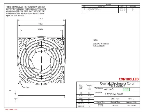
09121-G;中文规格书,Datasheet资料
- 格式:pdf
- 大小:170.35 KB
- 文档页数:2
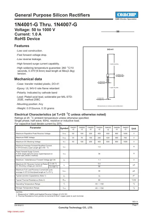
OElectrical Characteristics (at T A =25 C unless otherwise noted)ORatings at 25 C ambient temperature unless otherwise specified.Single phase, half wave, 60Hz, resistive or inductive load.For capacitive load derate current by 20%.ParameterSymbol UnitMaximum Repetitive Peak Reverse Voltage Maximum RMS Voltage Maximum DC Blocking VoltageMaximum Average Forward Rectified Current O 0.375"(9.5mm) Lead Length @T A =55C Peak Forward Surge Current, 8.3mS single half sine-wave superimposed on rated load (JEDEC method)Maximum Instantaneous Forward Voltage @1.0A Maximum DC Reverse Current at RatedOperating Temperature Range Storage Ttemperature RangeO T A =25C DC Blocking voltage per element Typical Junction Capacitance (Note 1)Typical Thermal Resistance (Note 2)503550V RRM V RMS V DC I (AV)I FSM V F I R C J R θJA T J T STG1.0305.0501560-55 ~ +150-55 ~ +150V V V AA V P FOC OCμA OC/WNOTES:1. Measured at 1.0MHz and Applied Reverse Voltage of 4.0V DC.22. Thermal Resistance from junction to terminal 6.0mm copper pads to each terminal.Voltage: 50 to 1000 V Current: 1.0 A RoHS DeviceFeatures-Low cost construction. -Fast forward voltage drop. -Low reverse leakage.-High forward surge current capability.O -High soldering temperature guarantee: 260C/10 seconds, 0.375”(9.5mm) lead length at 5lbs(2.3kg) tension.Mechanical data-Case: transfer molded plastic, DO-41 -Epoxy: UL 94V-0 rate flame retardant -Polarity: Indicated by cathode band-Lead: Plated axial lead, solderable per MIL-STD-202E, method 208C -Mounting position: Any-Weight: 0.012ounce, 0.33 grams10070100200140200400280400600420600800560800100070010001N4001-G Thru. 1N4007-G1.130-G 4001 1N -G 4002 1N -G 4003 1N -G 4004 1N -G 40051N -G 4006 1N -G 4007 1N O T A =100C Maximum Full Load Reverse Current,full cycle average 0.375”(9.5mm)lead length at T L =75 C O I R(AV)μARating and Characteristic Curves ( 1N4001) -G Thru. 4007-G1N Fig.2 Maximum. Non-Repetitive PeakForward Surge Current0ΙF S M , P e a k F o r w a r d S u r g e C u r r e n t (A )Number of Cycles at 60Hz1Fig.1 Typical Forward CurrentDerating CurveI (A V ), A v e r a g e F o r w a r d C u r r e n t (A )OT A , Ambient Temperature (C)02575175Fig.3 Typical Instantaneous ForwardCharacteristics0.01I F , I n s t a n t a n e o u s F o r w a r d C u r r e n t (A )V F , Instantaneous Forward Voltage (V)1.00.61.01.400.61.01.62.010015351.20.1Fig.4 Typical Reverse Characteristics0.01I R , I n s t a n t a n e o u s R e v e r s e C u r r e n t (m A )Percent of Peak Reverse Voltage (%)1.0100.11001250.40.80.81.8Fig.5 Typical Junction Capacitance10C J , C a p a c i t a n c e (p F )V R , Reverse Voltage (V)1000.11010010501500.21051025301.24080100140201206012010205025分销商库存信息: COMCHIP1N4002-G。
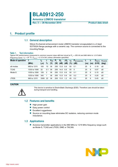
1. Product profile1.1General descriptionSilicon N-channel enhancement mode LDMOS transistor encapsulated in a 2-leadSOT502A flange package with a ceramic cap. The common source is connected to the mounting flange.1.2Features and benefitsHigh power gain Easy power controlExcellent ruggednessSource on mounting base eliminates DC isolators, reducing common mode inductance.1.3ApplicationsAvionics transmitter applications in the 960 MHz to 1215 MHz frequency range suchas Mode-S, TCAS and JTIDS, DME or TACAN.BLA0912-250Avionics LDMOS transistorRev. 3 — 26 November 2010Product data sheetTable 1.Test informationTypical RF performance measured in common source class-AB test circuit at P L =250W and 960MHz to 1215 MHz frequency band. T h = 25 °C; Z th(j-h) = 0.15 K/W; unless otherwise specified.Mode of operation f t p δV DS P L G p ΔG p ηD P droop(pulse)t r t f Z th(j-h)ϕins(rel)(MHz)(μs)%(V)(W)(dB)(dB)(%)(dB)(ns)(ns)(K/W)(deg)all modes 960 to 1215100103625013.50.8500.12560.18±5TCAS 1030 to 1090320.13625014.00.85002560.07±5Mode-S 1030 to 109012823625013.50.8500.12560.15±51030 to 109034013625013.50.8500.22560.20±5JTIDS 960 to 12153300223620013.0 1.2450.22560.45±5CAUTIONThis device is sensitive to ElectroStatic Discharge (ESD). Therefore care should be taken during transport and handling.2. Pinning information[1]Connected to flange.3. Ordering information4. Limiting values5. Thermal characteristics[1]Thermal resistance is determined under RF operating conditions; t p = 100 μs, δ = 10 %.Table 2.PinningPin Description Simplified outlineGraphic symbol1drain 2gate 3source[1]321sym039Table 3.Ordering informationType number Package NameDescriptionVersion BLA0912-250-flanged LDMOST ceramic package;2mounting holes; 2leadsSOT502ATable 4.Limiting valuesIn accordance with the Absolute Maximum Rating System (IEC 60134).Symbol ParameterConditionsMin Max Unit V DS drain-source voltage -75V V GS gate-source voltage -±22V P tot total power dissipation T h ≤25°C; t p =50μs; δ=2%-700W T stg storage temperature −65+150°C T jjunction temperature-200°CTable 5.Thermal characteristics Symbol ParameterConditions Typ Unit Z th(j-h)transient thermal impedance from junction toheatsinkT h = 25 °C[1]0.18K/W6. Characteristics6.1Ruggedness in class-AB operationThe BLA0912-250 is capable of withstanding a load mismatch corresponding to VSWR =5:1 through all phases under the following conditions: V DS =36V; f =960MHz to 1215MHz at rated load power.Table 6.DC characteristicsT j = 25 °C; per section unless otherwise specified.Symbol Parameter ConditionsMin Typ Max Unit V (BR)DSS drain-source breakdown voltage V GS =0V; I D =3mA75--V V GS(th)gate-source threshold voltage V DS =10 V; I D =300mA 4-5V I DSS drain leakage current V GS =0V; V DS =36V --1μA I DSX drain cut-off current V GS =V GSth +9V;V DS =10V45--A I GSS gate leakage current V GS =20V; V DS =0V --1μA g fs forward transconductanceV DS =10V; I D =10A-9-S R DS(on)drain-source on-state resistance V GS =9V; I D =10A-60-m ΩTable 7.RF characteristicsRF performance in common source class-AB circuit; T h = 25 °C; Z th = 0.15 K/W; unless otherwise specified.Symbol ParameterConditionsMin Typ Max Unit V DS drain-source voltage --36V f frequency 960-1215MHz P L output power t p =100μs; δ=10%250-W G p power gain P L =250W1213dB ηD drain efficiencyt p =100μs; δ=10%4050%Z th(j-h)transient thermal impedance from junction to heatsink t p =100μs; δ=10%--0.2K/W T hheatsink temperature −55-+70°C P droop(pulse)pulse droop power t p =100μs; δ=10%-0.10.5dB αresp(sp)spurious response VSWR load =2:1--−60dBc t r rise time -2550ns t ffall time-625ns7. Application information7.1Impedance informationTable 8.Typical impedanceTypical values per section unless otherwise specified.f Z S Z LMHzΩΩ9600.89−j1.70 1.53−j1.131030 1.37−j1.23 1.47−j0.991090 2.09−j1.27 1.38−j0.851140 2.40−j1.97 1.30−j0.711215 1.51−j2.61 1.17−j0.477.2Application circuitTable yout detailsSee Figure2.Striplines are on a Rodgers Duroid 6010 Printed-Circuit Board (PCB); εr = 10.2 F/m; thickness=0.64mmComponent Description DimensionsInput circuitL1stripline 5 mm × 0.8 mmC1stripline 1.2 mm × 3.5 mmL2stripline capacitor pad: 1 mm × 1 mm (1×)curve: width 0.8 mm; angle 90°; radius 0.8 mm (10×)vertical: 3.9 mm × 0.8 mm (2×)vertical: 9.4 mm × 0.8 mm (3×)horizontal: 0.5 mm × 0.8 mm (4×)L3stripline 3 mm × 2 mmC2stripline 4 mm × 6.5 mmL4stripline 5 mm × 1 mmC3stripline8.8 mm × 30 mm + 0.2 mm × 13 mmOutput circuitC4stripline0.2 mm × 13 mm + 19 mm × 17.1 mmL5stripline 2.5 mm × 2.3 mmL6stripline 4 mm × 1 mmC5stripline 3 mm × 6.6 mmL7stripline curve: width 0.8 mm; angle 90°; radius 0.8 mm (6×)vertical: 2.2 mm × 0.8 mm (2×)vertical: 6 mm × 0.8 mm (1×)horizontal: 1 mm × 0.8 mm (2×)L8stripline 2.5 mm × 0.8 mm1/4 λ line stripline curve: width 1 mm; angle 90°; radius 0.8 mmvertical: 5 mm × 1 mmhorizontal: 19 mm × 1 mmTable 10.List of componentsSee Figure3.Component Description Value RemarksC1,C3, C9multilayer ceramic chip capacitor 1 nF[1]C2, C6, C10multilayer ceramic chip capacitor22 pF[2]C4tantalum SMD capacitor47μF; 20 V KEMET: T491D476M020AS C5multilayer ceramic chip capacitor56 pF[2]C7multilayer ceramic chip capacitor47 pF[2]C8tantalum SMD capacitor22μF; 63 VR1SMD resistor51Ω0805R2resistor49.9Ω[1]American Technical Ceramics type 100B or capacitor of same quality.[2]American Technical Ceramics type 100A or capacitor of same quality.8. Test information8.1RF performanceTypical RF performance measured in common source class-AB test circuit at P L=250Wand 960MHz to 1215 MHz frequency band. T h = 25 °C; Z th(j-h) = 0.15 K/W; unlessotherwise specified.9. Package outlineFlanged LDMOST ceramic package; 2 mounting holes; 2 leads SOT502AFig 8.Package outline SOT502A10. Abbreviations11. Revision historyTable 11.AbbreviationsAcronym Description DC Direct CurrentDME Distance Measuring EquipmentJTIDS Joint Tactical Information Distribution System LDMOS Laterally Diffused Metal-Oxide SemiconductorLDMOST Laterally Diffused Metal-Oxide Semiconductor Transistor Mode-S Mode Select RF Radio Frequency SMD Surface Mounted Device TACAN TACtical Air NavigationTCAS Traffic Collision Avoidance System VSWRVoltage Standing-Wave RatioTable 12.Revision historyDocument ID Release date Data sheet status Change notice Supersedes BLA0912-250 v.320101126Product data sheet-BLA0912-250_2Modifications:•The format of this data sheet has been redesigned to comply with the new identity guidelines of NXP Semiconductors.•Legal texts have been adapted to the new company name where appropriate.•Table 10 on page 6: The remark of component C8 has been removed.•Table 10 on page 6: The value of component C8 has been specified in more detail.BLA0912-250_220040722Product data sheet -BLA0912-250_N_1BLA0912-250_N_120031024Preliminary data sheet-939775012224分销商库存信息: NXPBLA0912-250,112。
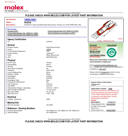
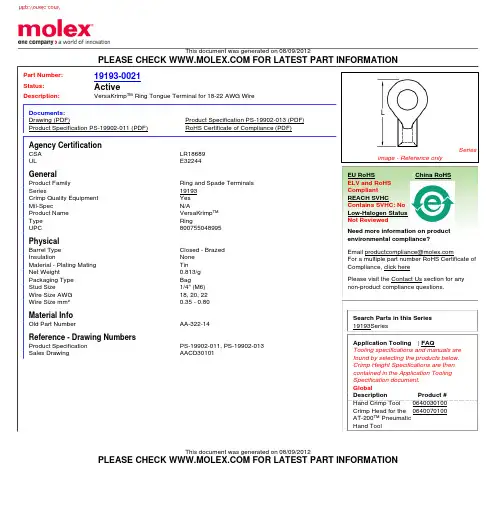
This document was generated on 08/13/2012PLEASE CHECK FOR LATEST PART INFORMATIONPart Number:19002-0021Status:ActiveDescription:Avikrimp™ Fully Insulated Quick Disconnect, Female, for 18-22 AWG Wire, BoxDocuments:Drawing (PDF)Product Specification PS-19902-014 (PDF)Product Specification PS-19902-011 (PDF)RoHS Certificate of Compliance (PDF)Product Specification PS-19902-013 (PDF)Agency CertificationULE79133GeneralProduct Family Quick Disconnects Series19002Crimp Quality Equipment YesProduct Name Avikrimp™Type Quick Disconnect UPC800753027244PhysicalBarrel Type Closed Flammability 94V-2GenderFemale Glow-Wire Compliant NoInsulationNylon (PA)Lock to Mating Part None Material - Metal Brass Net Weight 0.853/g OrientationStraight Packaging TypeBag Polarized to Mating Part NoTab Thickness 0.81mm Tab Width5.21mmTemperature Range - Operating -65°C to +105°C Wire Insulation Diameter 3.17mm max.Wire Size AWG 18, 20, 22Wire Size mm²0.35 - 0.80ElectricalVoltage - Maximum300V Material InfoOld Part NumberAA-5285Reference - Drawing NumbersProduct SpecificationPS-19902-011, PS-19902-013, PS-19902-014Sales DrawingSD-19002-003Seriesimage - Reference onlyEU RoHSChina RoHSELV and RoHS Compliant REACH SVHC Not ReviewedLow-Halogen Status Not ReviewedNeed more information on product environmental compliance?Email productcompliance@For a multiple part number RoHS Certificate of Compliance, click herePlease visit the Contact Us section for any non-product compliance questions.Search Parts in this Series 19002SeriesApplication Tooling | FAQTooling specifications and manuals are found by selecting the products below.Crimp Height Specifications are then contained in the Application Tooling Specification document.GlobalDescription Product #Crimp Head for the AT-200™ Pneumatic Hand Tool0640050800Hand Crimp Tool 0640010800This document was generated on 08/13/2012PLEASE CHECK FOR LATEST PART INFORMATION/分销商库存信息: MOLEX 0190020021。