BC879,112;BC875,126;中文规格书,Datasheet资料
- 格式:pdf
- 大小:72.05 KB
- 文档页数:8

Data and signal line chokesCommon-mode chokes, ring core0.005 … 47 mH, 100 … 1200 mA, 60 °CSeries/Type:B82793C0/S0Date:July 2010¤ EPCOS AG 2010. Reproduction, publication and dissemination of this publication, enclosures hereto and the information contained therein without EPCOS’ prior express consent is prohibited.Rated voltage 42 V AC/80 V DCRated inductance 0.005 mH to 47 mH Rated current 100 mA to 1200 mA Construction■Current-compensated double choke ■Ferrite core■LCP case (UL 94 V-0), silicone potting ■Bifilar winding (B82793C0)■Sector winding (B82793S0)Features■High rated currents, reduced components height ■Qualified to AEC-Q200 (L d 4.7 mH)■Suitable for reflow soldering ■RoHS-compatibleFunction■B82793C0:Suppression of asymmetrical interference coupled in on lines,whereas data signals up to some MHz can pass unaffectedly.■B82793S0:Suppression of asymmetrical and symmetrical interference (by L stray )coupled in on lines. The high-frequency portions of the symmetrical data signal are decreased so far that EMC problems can be significantly reduced.Applications■Automotive applications, e.g. CAN bus ■Industrial applications■Types with L R ! 4.7 mH only for telecom applicationsTerminals■Base material CuSn6■Layer composition Ni, Sn ■Hot-dippedMarking■Marking on component: Manufacturer, process location (coded),winding method (coded), ordering code (short form), date of manufacture (YWWD)■Minimum data on reel: Manufacturer, ordering code,L value and tolerance, quantity, date of packing Delivery mode and packing unit■16-mm blister tape, wound on 330-mm reel ■Packing unit: 1500 pcs./reel Common-mode chokes, ring coreDimensional drawing and pin configurationLayout recommendationTaping and packing Blister tapeReelDimensions in mmDimensions in mmCommon-mode chokes, ring coreCommon-mode chokes, ring coreTechnical data and measuring conditionsRated voltage V R42 V AC (50/60 Hz) / 80 V DCRated temperature T R60 °CRated current I R Referred to 50 Hz and rated temperatureRated inductance L R Measured with Agilent 4284A, 0.1 mA, 20 °CMeasuring frequency:L R d 1 mH = 100 kHzL R! 1 mH = 10 kHzInductance is specified per winding.Inductance tolerance r30% (L R d0.47mH), –30/+50% (L R t1mH) at 20 °C Inductance decrease 'L/L 10% at DC magnetic bias with I R, 20 °CStray inductance L stray,typ Measured with Agilent 4284A, 5 mA, 20 °C, typical valuesMeasuring frequency:L R d 11 P H = 1 MHzL R! 11 P H = 100 kHzDC resistance R typ Measured at 20q C, typical values, specified per winding Solderability SnPb:(215 r3) °C, (3 r0.3) sSn96.5Ag3.0Cu0.5:(245 r5) °C, (3 r0.3) sWetting of soldering area t 95%(to IEC 60068-2-58)Resistance to soldering heat(260 r5) °C, (10 r1) s (to IEC 60068-2-58)Climatic category 40/125/56 (to IEC 60068-1)Storage conditions (packaged)–25 °C … +40 °C, d 75% RHWeight Approx. 0.25 gCharacteristics and ordering codes Sample kit available. Ordering code: B82793X001.For more information refer to chapter “Sample kits”.L R mH L stray,typ nH I R mA R typ m :V test V DC, 2 s Ordering code 0.005 40120060250B82793C0502N2010.011 50 80080250B82793C0113N2010.025 60 800110250B82793C0253N2010.0251400 800110250B82793S0253N2010.051 70 800140250B82793C0513N2010.0512300 800140250B82793S0513N2010.10 100 500180250B82793C0104N2010.47 100 700170750B82793C0474N2151.0 70 700140750B82793C0105N2652.2 120 500400750B82793C0225N2654.7 250 400550750B82793C0475N265For telecommunications203001001800750B82793C0206N2654712001003700750B82793C0476N265Common-mode chokes, ring coreInsertion loss D (typical values at |Z| = 50 :, 20 °C)asymmetrical, all branches in parallel (common mode)symmetrical (differential mode)L R = 0.005 mHL R = 0.025 mH (low L stray)L R = 0.011 mHL R = 0.025 mH (high L stray)Common-mode chokes, ring coreInsertion loss D (typical values at |Z| = 50 :, 20 °C)asymmetrical, all branches in parallel (common mode)symmetrical (differential mode)L R = 0.051 mH (low L stray) L R = 0.10 mH L R = 0.051 mH (high L stray) L R = 0.47 mHCommon-mode chokes, ring coreInsertion loss D (typical values at |Z| = 50 :, 20 °C)asymmetrical, all branches in parallel (common mode)symmetrical (differential mode)L R =1.0 mH L R = 4.7 mH L R = 2.2 mH L R = 20 mHCommon-mode chokes, ring coreInsertion loss D (typical values at |Z| = 50 :, 20 °C)asymmetrical, all branches in parallel (common mode)symmetrical (differential mode)L R = 47 mH Current derating I op/I R versus ambient temperatureCommon-mode chokes, ring coreRecommended reflow soldering curvePb containing solder material (based on CECC 00802 edition 2)Pb-free solder material (based on JEDEC J-STD 020C)Time from 25 °C to T 4: max 300 s Maximal numbers of reflow cycles: 3T 1°C T 2°C T 3°C T 4°C t 1s t 2s t 3s150200217250< 110< 90< 40 @ T 4 –5 °CCommon-mode chokes, ring core分销商库存信息:EPCOSB82793S0513N201B82793C475N265。
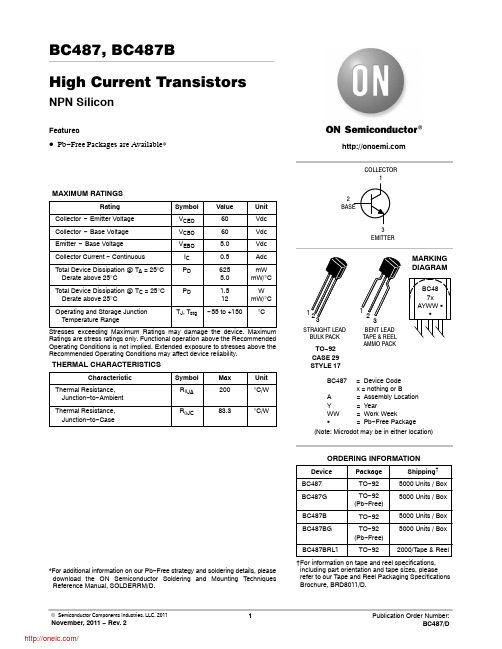
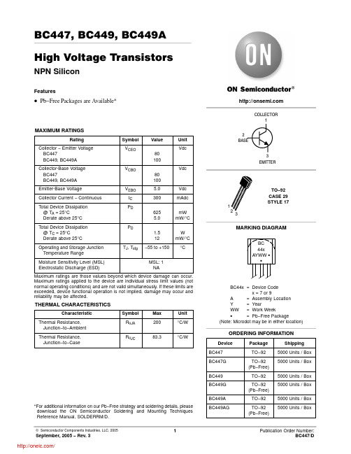
BC487, BC487BHigh Current TransistorsNPN SiliconFeatures•Pb −Free Packages are Available*MAXIMUM RATINGSRatingSymbol Value Unit Collector − Emitter Voltage V CEO 60Vdc Collector − Base Voltage V CBO 60Vdc Emitter − Base Voltage V EBO 5.0Vdc Collector Current − Continuous I C 0.5Adc Total Device Dissipation @ T A = 25°C Derate above 25°CP D 6255.0mW mW/°C Total Device Dissipation @ T C = 25°C Derate above 25°CP D 1.512W mW/°COperating and Storage JunctionTemperature RangeT J , T stg−55 to +150°CStresses exceeding Maximum Ratings may damage the device. Maximum Ratings are stress ratings only. Functional operation above the Recommended Operating Conditions is not implied. Extended exposure to stresses above the Recommended Operating Conditions may affect device reliability.THERMAL CHARACTERISTICSCharacteristicSymbol Max Unit Thermal Resistance,Junction −to −Ambient R q JA 200°C/W Thermal Resistance,Junction −to −CaseR q JC83.3°C/W*For additional information on our Pb−Free strategy and soldering details, please download the ON Semiconductor Soldering and Mounting Techniques Reference Manual, SOLDERRM/D.Device Package Shipping †ORDERING INFORMATIONBC487TO −925000 Units / Box BC487B TO −925000 Units / Box BC487BRL1TO −922000/Tape & ReelMARKING DIAGRAMCOLLECTOR23EMITTERBC487x AYWW GG†For information on tape and reel specifications,including part orientation and tape sizes, please refer to our Tape and Reel Packaging Specifications Brochure, BRD8011/D.BC487G TO −92(Pb −Free)5000 Units / Box BC487=Device Code x = nothing or BA =Assembly Location Y =Year WW =Work Week G =Pb −Free Package(Note: Microdot may be in either location)BC487BG TO −92(Pb −Free)5000 Units / Box TO −92CASE 29STYLE 17BENT LEAD TAPE & REEL AMMO PACKSTRAIGHT LEAD BULK PACKELECTRICAL CHARACTERISTICS (T A = 25°C unless otherwise noted)CharacteristicSymbolMinTypMaxUnitOFF CHARACTERISTICSCollector −Emitter Breakdown Voltage (Note 1)(I C = 10 mAdc, I B = 0)V (BR)CEO 60−−Vdc Collector −Base Breakdown Voltage (I C = 100 m Adc, I E = 0)V (BR)CBO 60−−Vdc Emitter −Base Breakdown Voltage (I E = 10 m Adc, I C = 0)V (BR)EBO 5.0−−Vdc Collector Cutoff Current (V CB = 40 Vdc, I E = 0)I CBO−−100nAdcON CHARACTERISTICS*DC Current Gain(I C = 10 mAdc, V CE = 2.0 Vdc)(I C = 100 mAdc, V CE = 2.0 Vdc)BC487BC487B(I C = 1.0 Adc, V CE = 5.0 Vdc)*h FE406016015−−260−−400400−−Collector −Emitter Saturation Voltage (I C = 500 mAdc, I B = 50 mAdc)(I C = 1.0 Adc, I B = 100 mAdc)V CE(sat)−−0.20.30.5−VdcBase −Emitter Saturation Voltage (I C = 500 mAdc, I B = 50 mAdc)(I C = 1.0 Adc, I B = 100 mAdc)(1)V BE(sat)−−0.850.91.2−VdcDYNAMIC CHARACTERISTICSCurrent −Gain − Bandwidth Product(I C = 50 mAdc, V CE = 2.0 Vdc, f = 100 MHz)f T −200−MHz Output Capacitance(V CB = 10 Vdc, I E = 0, f = 1.0 MHz)C ob −7.0−pF Input Capacitance(V EB = 0.5 Vdc, I C = 0, f = 1.0 MHz)Cib−50−pF1.Pulse Test: Pulse Width = 300 m s, Duty Cycle2.0%.Figure 1. Switching Time Test Circuits*Total Shunt Capacitance of Test Jig and Connectors For PNP T est Circuits, Reverse All Voltage PolaritiesTURN-ON TIME V OUTPUTS < 6.0 pFTURN-OFF TIME +V V OUTPUTS < 6.0 pFt r = 3.0 nsFigure 2. Current −Gain − Bandwidth Product I C , COLLECTOR CURRENT (mA)f , C U R R E N T -G A I N — B A N D W I D T H P R O D U C T (M H z )T C , C A P A C I T A N C E (p F )t , T I M E (n s )Figure 3. CapacitanceV R , REVERSE VOLTAGE (VOLTS)80Figure 4. Switching TimeI C , COLLECTOR CURRENT (mA)1.0 k Figure 5. Thermal Responset, TIME (ms)1.0r (t ) T R A N S I E N T T H E R M A L R E S I S T A N C E (N O R M A L I Z E D )0.010.020.030.050.070.10.20.50.750 kV CE , COLLECTOR-EMITTER VOLTAGE (VOLTS)1.0 kI C , C O L L E C T O R C U R R E N T (m A )Figure 6. Active Region − Safe Operating Area7005003002001007050302010Figure 7. DC Current GainI C , COLLECTOR CURRENT (mA)4000.50.7 1.0 2.0 3.0 5.07.01020305070100200200100806040h F E , D C C U R R E N T G A I N 300500I C , COLLECTOR CURRENT (mA)Figure 8. “On” Voltages V , V O L T A G E (V O L T S )0I C , COLLECTOR CURRENT (mA)Figure 9. Collector Saturation RegionV C E , C O L L E C T O R -E M I T T E R V O L T A G E (V O L T S )1.00.60.40.20I C , COLLECTOR CURRENT (mA)Figure 10. Base −Emitter Temperature Coefficient -0.8-2.8-1.2-1.6-2.0-2.4R V B , T E M P E R A T U R E C O E F F I C I E N T (m V /C )°θI C , COLLECTOR CURRENT (mA)Figure 11. “On” VoltagesV , V O L T A G E (V O L T S )-1.0-0.8-0.6-0.4-0.2I B , BASE CURRENT (mA)Figure 12. Collector Saturation Region V C E , C O L L E C T O R -E M I T T E R V O L T A G E (V O L T S )-1.0-0.8-0.6-0.4-0.2I C , COLLECTOR CURRENT (mA)Figure 13. Base −Emitter Temperature CoefficientR V B , T E M P E R A T U R E C O E F F I C I E N T (m V /C )°θPACKAGE DIMENSIONSTO −92(TO −226)CASE 29−11ISSUE AMSTYLE 17:PIN 1.COLLECTOR2.BASE3.EMITTERNOTES:1.DIMENSIONING AND TOLERANCING PER ANSI Y14.5M, 1982.2.CONTROLLING DIMENSION: INCH.3.CONTOUR OF PACKAGE BEYOND DIMENSION R IS UNCONTROLLED.4.LEAD DIMENSION IS UNCONTROLLED IN P AND BEYOND DIMENSION K MINIMUM.SECTION X −XDIM MIN MAX MIN MAX MILLIMETERSINCHES A 0.1750.205 4.45 5.20B 0.1700.210 4.32 5.33C 0.1250.165 3.18 4.19D 0.0160.0210.4070.533G 0.0450.055 1.15 1.39H 0.0950.105 2.42 2.66J 0.0150.0200.390.50K 0.500---12.70---L 0.250--- 6.35---N 0.0800.105 2.04 2.66P ---0.100--- 2.54R 0.115--- 2.93---V0.135--- 3.43---NOTES:1.DIMENSIONING AND TOLERANCING PER ASME Y14.5M, 1994.2.CONTROLLING DIMENSION: MILLIMETERS.3.CONTOUR OF PACKAGE BEYOND DIMENSION R IS UNCONTROLLED.4.LEAD DIMENSION IS UNCONTROLLED IN P AND BEYOND DIMENSION K MINIMUM.SECTION X −XDIM MIN MAX MILLIMETERS A 4.45 5.20B 4.32 5.33C 3.18 4.19D 0.400.54G 2.40 2.80J 0.390.50K 12.70---N 2.04 2.66P 1.50 4.00R 2.93---V3.43---STRAIGHT LEAD BULK PACKBENT LEADTAPE & REEL AMMO PACKON Semiconductor and are registered trademarks of Semiconductor Components Industries, LLC (SCILLC). SCILLC reserves the right to make changes without further notice to any products herein. SCILLC makes no warranty, representation or guarantee regarding the suitability of its products for any particular purpose, nor does SCILLC assume any liability arising out of the application or use of any product or circuit, and specifically disclaims any and all liability, including without limitation special, consequential or incidental damages.“Typical” parameters which may be provided in SCILLC data sheets and/or specifications can and do vary in different applications and actual performance may vary over time. All operating parameters, including “Typicals” must be validated for each customer application by customer’s technical experts. SCILLC does not convey any license under its patent rights nor the rights of others. SCILLC products are not designed, intended, or authorized for use as components in systems intended for surgical implant into the body, or other applications intended to support or sustain life, or for any other application in which the failure of the SCILLC product could create a situation where personal injury or death may occur. Should Buyer purchase or use SCILLC products for any such unintended or unauthorized application, Buyer shall indemnify and hold SCILLC and its officers, employees, subsidiaries, affiliates,and distributors harmless against all claims, costs, damages, and expenses, and reasonable attorney fees arising out of, directly or indirectly, any claim of personal injury or death associated with such unintended or unauthorized use, even if such claim alleges that SCILLC was negligent regarding the design or manufacture of the part. SCILLC is an Equal Opportunity/Affirmative Action Employer. This literature is subject to all applicable copyright laws and is not for resale in any manner.PUBLICATION ORDERING INFORMATION分销商库存信息:ONSEMIBC487BG BC487BRL1BC487G。
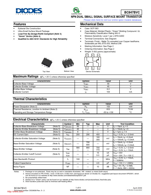
NPN DUAL SMALL SIGNAL SURFACE MOUNT TRANSISTORFeatures• Epitaxial Die Construction• Ultra-Small Surface Mount Package• Lead Free By Design/RoHS Compliant (Note 3) • "Green" Device (Note 4)•Qualified to AEC-Q101 Standards for High ReliabilityMechanical Data• Case: SOT-563 • Case Material: Molded Plastic, "Green" Molding Compound. ULFlammability Classification Rating 94V-0 • Moisture Sensitivity: Level 1 per J-STD-020D • Terminal Connections: See Diagram • Terminals: Finish - Matte Tin annealed over Copper leadframe.Solderable per MIL-STD-202, Method 208 • Marking Information: See Page 2 • Ordering Information: See Page 2 • Weight: 0.002 grams (approximate)Maximum Ratings @T A = 25°C unless otherwise specifiedCharacteristicSymbol Value Unit Collector-Base Voltage V CBO 50 V Collector-Emitter Voltage V CEO 45 V Emitter-Base Voltage V EBO 6.0 V Collector Current I C100mAThermal CharacteristicsCharacteristicSymbol Value Unit Power Dissipation (Note 2)P D 150 mW Thermal Resistance, Junction to Ambient (Note 2) R θJA 833 °C/W Operating and Storage Temperature Range T J , T STG-55 to +150°CElectrical Characteristics @T A = 25°C unless otherwise specifiedCharacteristicSymbol Min Typ Max UnitTest ConditionCollector-Base Breakdown Voltage (Note 5) V (BR)CBO 50 — — V I C = 10μA, I B = 0 Collector-Emitter Breakdown Voltage (Note 5) V (BR)CEO 45 — — V I C = 10mA, I B = 0 Emitter-Base Breakdown Voltage (Note 5) V (BR)EBO 6 — — V I E = 1μA, I C = 0DC Current Gain (Note 5) h FE 200 290 450 — V CE = 5.0V, I C = 2.0mA Collector-Emitter Saturation Voltage (Note 5) V CE(SAT) — — 100 300 mV I C = 10mA, I B = 0.5mA I C = 100mA, I B = 5.0mA Base-Emitter Saturation Voltage (Note 5) V BE(SAT) — 700 900 — mV I C = 10mA, I B = 0.5mA I C = 100mA, I B = 5.0mA Base-Emitter Voltage (Note 5) V BE 580 — 660 — 700 770 mV V CE = 5.0V, I C = 2.0mA V CE = 5.0V, I C = 10mA Collector-Emitter Cutoff Current (Note 5) I CBO I CBO — — 15 5.0 nA µA V CB = 30VV CB = 30V, T A = 150°C Gain Bandwidth Product f T 100 — — MHz V CE = 5.0V, I C = 10mA, f = 100MHzOutput Capacitance C OBO — — 4.5 pF V CB = 10V, f = 1.0MHz Noise FigureNF——10dBV CE = 5V, R S = 2.0k Ω, f = 1.0kHz, BW = 200HzNotes:1. Package is non-polarized. Parts may be on reel in orientation illustrated, 180° rotated, or mixed (both ways).2. Device mounted on FR-4 PCB, 1 inch x 0.85 inch x 0.062 inch; pad layout as shown on Diodes Inc. suggested pad layout document AP02001, which can be found on our website at /datasheets/ap02001.pdf.3. No purposefully added lead.4. Diodes Inc's "Green" policy can be found on our website at /products/lead_free/index.php5. Short duration pulse test used to minimize self-heating effect.Top View Bottom ViewDevice SchematicC 1B 2E 2C 2E 1B 1Please click here to visit our online spice models database.050100150250200150500T , AMBIENT TEMPERATURE (C)Fig. 1 Power Dissipation vs. Ambient Temperature (Note 2)A °P , P O W E R D I S S I P A T I O N (m W )Dh D C C U R R E N T G A I NF E ,I , COLLECTOR CURRENT (mA)Fig. 2 Typical DC Current Gain vs. Collector Current CV , C O L L E C T O R -E M I T T E RS A T U R A T I O N V O L T A G E (V )C E (S A T )I , COLLECTOR CURRENT (mA)Fig. 3 Typical Collector Emitter Saturation Voltagevs. Collector CurrentCf , G A I N -B A N D W I D T H P R O D U C T (M H z )T I , COLLECTOR CURRENT (mA)Fig. 4 Typical Gain-Bandwidth Product vs. Collector Current COrdering Information (Note 6)Part Number Case Packaging BC847BVC-7SOT-563 3000/Tape & ReelNotes:6. For packaging details, go to our website at /datasheets/ap02007.pdf.Marking InformationDate Code KeyYear 2005 2006 2007 2008 2009 2010 2011 2012 2013 2014 2015 Code S T U V W X Y Z A B CMonth Jan Feb Mar Apr May Jun Jul Aug Sep Oct Nov Dec Code 1 2 3 4 5 6 7 8 9 O N D4VK = Product Type Marking Code YM = Date Code MarkingY = Year (ex: S = 2005)M = Month (ex: 9 = September) 4VK YMPackage Outline DimensionsSuggested Pad LayoutSOT-563Dim Min Max Typ A 0.15 0.30 0.20 B 1.10 1.25 1.20 C 1.55 1.70 1.60 D - - 0.50 G 0.90 1.10 1.00 H 1.50 1.70 1.60 K 0.55 0.60 0.60 L 0.100.30 0.20 M 0.10 0.18 0.11 All Dimensions in mmDimensions Value (in mm)Z 2.2 G 1.2 X 0.375 Y 0.5 C1 1.7 C2 0.5XZYC1C2C2GIMPORTANT NOTICEDIODES INCORPORATED MAKES NO WARRANTY OF ANY KIND, EXPRESS OR IMPLIED, WITH REGARDS TO THIS DOCUMENT, INCLUDING, BUT NOT LIMITED TO, THE IMPLIED WARRANTIES OF MERCHANTABILITY AND FITNESS FOR A PARTICULAR PURPOSE (AND THEIR EQUIVALENTS UNDER THE LAWS OF ANY JURISDICTION).Diodes Incorporated and its subsidiaries reserve the right to make modifications, enhancements, improvements, corrections or other changes without further notice to this document and any product described herein. Diodes Incorporated does not assume any liability arising out of the application or use of this document or any product described herein; neither does Diodes Incorporated convey any license under its patent or trademark rights, nor the rights of others. Any Customer or user of this document or products described herein in such applications shall assume all risks of such use and will agree to hold Diodes Incorporated and all the companies whose products are represented on Diodes Incorporated website, harmless against all damages.Diodes Incorporated does not warrant or accept any liability whatsoever in respect of any products purchased through unauthorized sales channel. Should Customers purchase or use Diodes Incorporated products for any unintended or unauthorized application, Customers shall indemnify and hold Diodes Incorporated and its representatives harmless against all claims, damages, expenses, and attorney fees arising out of, directly or indirectly, any claim of personal injury or death associated with such unintended or unauthorized application.Products described herein may be covered by one or more United States, international or foreign patents pending. Product names and markings noted herein may also be covered by one or more United States, international or foreign trademarks.LIFE SUPPORTDiodes Incorporated products are specifically not authorized for use as critical components in life support devices or systems without the express written approval of the Chief Executive Officer of Diodes Incorporated. As used herein:A. Life support devices or systems are devices or systems which:1. are intended to implant into the body, or2. support or sustain life and whose failure to perform when properly used in accordance with instructions for use provided in thelabeling can be reasonably expected to result in significant injury to the user.B. A critical component is any component in a life support device or system whose failure to perform can be reasonably expected to cause the failure of the life support device or to affect its safety or effectiveness.Customers represent that they have all necessary expertise in the safety and regulatory ramifications of their life support devices or systems, and acknowledge and agree that they are solely responsible for all legal, regulatory and safety-related requirements concerning their products and any use of Diodes Incorporated products in such safety-critical, life support devices or systems, notwithstanding any devices- or systems-related information or support that may be provided by Diodes Incorporated. Further, Customers must fully indemnify Diodes Incorporated and its representatives against any damages arising out of the use of Diodes Incorporated products in such safety-critical, life support devices or systems.Copyright © 2009, Diodes Incorporated分销商库存信息: DIODESBC847BVC-7。
BC817-25BC817-40SMALL SIGNAL NPN TRANSISTORSPRELIMINARY DATAsSILICON EPITAXIAL PLANAR NPN TRANSISTORSsMINIATURE SOT-23 PLASTIC PACKAGE FOR SURFACE MOUNTING CIRCUITS s TAPE AND REEL PACKINGsTHE PNP COMPLEMENTARY TYPES ARE BC807-25 AND BC817-40 RESPECTIVELYAPPLICATIONS s WELL SUITABLE FOR PORTABLE EQUIPMENTs SMALL LOAD SWITCH TRANSISTORS WITH HIGH GAIN AND LOW SATURATION VOLTAGE®September 2002ABSOLUTE MAXIMUM RATINGS1/4Pr od u c t (s ) -Ob so l e t ePr od u c t (s ) -O bs oTHERMAL DATAELECTRICAL CHARACTERISTICS (T case = 25 o C unless otherwise specified)BC817-25 / BC817-40BC817-25 / BC817-40Ob so l e t ePr od u c t (s ) -O bs o l e t eP r od u c t (s) Information furnished is believed to be accurate and reliable. However, STMicroelectronics assumes no responsibility for the consequences of use of such information nor for any infringement of patents or other rights of third parties which may result from its use. No license is granted by implication or otherwise under any patent or patent rights of STMicroelectronics. Specification mentioned in this publication are subject to change without notice. This publication supersedes and replaces all information previously supplied. STMicroelectronics products are not authorized for use as critical components in life support devices or systems without express written approval of STMicroelectronics.The ST logo is a trademark of STMicroelectronics © 2002 STMicroelectronics – Printed in Italy – All Rights ReservedSTMicroelectronics GROUP OF COMPANIESAustralia - Brazil - Canada - China - Finland - France - Germany - Hong Kong - India - Israel - Italy - Japan - Malaysia - Malta - Morocco - Singapore - Spain - Sweden - Switzerland - United Kingdom - United States.BC817-25 / BC817-40分销商库存信息: STMBC817-40。
CAT.NO.1209(Screw Installed)CAT.NO.1207(Screw Supplied Unassembled)CAT.NO.1205(No Screw Supplied)CAT.NO.1283(Screw Installed)CAT.NO.1208(Screw Supplied Unassembled)CAT.NO.1206(No Screw Supplied)CAT.NO.1299(Screw Supplied Unassembled)CAT.NO.1202(Screw Installed &Captivated)CAT.NO.1201(Screw Installed &Captivated)CAT.NO.1298(Screw Supplied Unassembled)S C R E W T E R M I N A L S66HEAVY DUTY SCREW TERMINALS -30AMPThese sturdy,low cost screw terminals,feature an anti-rotation tab for use with spade terminals.They are available with the screw installed and captivated,the screw unassembled or without a screw..093[2.36].187[4.8].406[10.3].375[9.6].437[11.1]DIA..250[6.4].125[3.2]10-32 x .250 [6.3] L.SCREW.156[4.0]PRINCIPLE FEATURES•Easy to connect using solid or stranded wire,crimp lugs or terminals•Anti-rotation tab for use with spade terminals •Supplied with screw installed and captivated,with screw unassembled,or without screw •Stainless steel screw will not wickSPECIFICATIONSRated:15AmpsTerminal:.032(.81)Brass,Matte Tin Plate Screw:Combination drive,Stainless SteelSPECIFICATIONSRated:30AmpsTerminal:.062(1.6)Brass,Matte Tin Plate Screw:Combination drive,Stainless SteelMounting DetailMounting DetailThese heavy duty terminals are available with the screw installed or unassembled,and feature easy access to connect solid or stranded wire,crimp type lugs or terminals..375 [9.5]DIA.8-32 x .375 [9.5] L.SCREW.115 [2.9].531[13.5].437[11.1].140[3.6].297[7.6].406 [10.3].109[2.8]45°45°.109[2.8].406 [10.3].297[7.6].140[3.6].437[11.1].531[13.5].115 [2.9]10-32 x .375 [9.5] L.SCREW.375 [9.5]DIA..210 [5.3] DIA..077 [1.96].126 [3.2].470[12.0]SPECIFICATIONSRated:15AmpsTerminal:.064(1.6)Brass,Matte Tin Plate Screw:Brass,Nickel PlateSPECIFICATIONSRated:30AmpsTerminal:.064(1.6)Brass,Matte Tin Plate Screw:Steel,Nickel PlateMounting Detail.470[12.0].126 [3.2].077[1.96].210 [5.3] DIA.Mounting DetailPRINCIPLE FEATURES•Anti-rotation tab for use with spade terminals•Below the board notched leg,to facilitate mechanical and solder connections•Easy to connect using solid or stranded wire,crimp lugs or terminals•Available with screw installed,unassembled,or without screw.187[4.7]DIA..110[2.8].340[8.7].210 [5.3] DIA..075[1.9].142[3.6].472 [12.0].156[4.0].328[8.4].187 [4.8].094 [2.4].375 [9.5]DIA..100[2.6].062 [1.57]6-32x .250[6.3] L.SCREWLOW PROFILE SCREW TERMINALS10-328-32CAT.NO.1284(No Screw Supplied)CAT.NO.1293(No Screw Supplied)10-326-32Tel (718)956-8900•Fax (718)956-9040(800)221-5510•kec@31-0720th Road –Astoria,NY 11105-2017RoHS COMPLIANT ~ISO 9001CERTIFIED®THRU HOLECAT.NO.8730(Screw Installed).102 [2.6].039[1.00]DIA..187 [4.8].197 [5.0].157[4.0]SQUAREM2.5 x .156[4.0]L.SCREW.110 [2.8] DIA.HOLE THRUSPECIFICATIONSTerminal:Brass,Tin Plate Screw:Steel,Zinc Plate Mounting Hole:.047(1.2)Current Rating:15AMPWIRE CONTACTCAT.NO.8737(Screw Installed)CONTACT .197[5.0].039[1.0].192[4.9].105[2.7]DIA.THRU..158[4.0]SQUAREM2.5X 4.0L.SCREWSPECIFICATIONSTerminal:Brass,Tin Plate Screw:Steel,Zinc PlateContact:Phoshorus Bronze,Tin Plate Mounting Hole:.047(1.2)Current Rating:15AMP分销商库存信息: KEYSTONE-ELECTRONICS 12061205。