Overview and Challenges of Thin Film Solar Electric Technologies
- 格式:pdf
- 大小:379.18 KB
- 文档页数:7

Thin-film silicon PV technology2012-2013 ICARE course on Fundamentals of Solar Energy Joaquim Nassar, Romain Cariou, Jean-Christophe DornstetterCourse overview update –Week2Monday Tuesday Wednesday Thursday Friday4. March5. March6. March7. March8. March8h30-9h45Lecture -NassarAlternatives tocrystalline silicon Lecture -NassarIntroduction to thin-filmsilicon technologyLecture and exercise -MayerSolar resourceLecture and exercise -MayerPV systemsLecture and exercise-MayerPV systemsinvited talk of Pr Roca ICabarrocasHomeworksolutionExercise -Nassar, Cariou, Dornstetter Elementary 11h-12hExercise Cariou-Question andanswer sessionElementary calculations on semiconductors Exercise –Cariou, DornstetterPC1D optimization work, cont’d14h-16h Exercise -Nassar,Cariou, Dornstettersolar cell optimizationwith PC1D Homework preparationHomework -Design ofan antireflectiontiinvited talk of PrKaare SandholtLecture and exercise -MayerPV systemsFinal Quiz (undersupervision ofICARE staff)30%f th d coating PV systems30% of the grade(70% : finalexamination at endof semester)Outline•Silicon thin films today : products and market•Plasma-enhanced chemical vapor deposition Plasma enhanced chemical vapor deposition•Hydrogenated Amorphous Silicon (a-Si:H)Si H b d PV l ll•a-Si:H based PV solar cells•Heterojunction technology•From amorphous to thin-film crystalline siliconRange of applications of silicon thin films :“Wide-area electronics”“Wid l t i”Flexible thin-film silicon modules («roll-to-roll» manufacturing)»manufacturing)Reminder : crystalline silicon module manufacturingMetallurgical Grade SiStar t SiHCl 3SiH 4GasSiemens FBR PyrolysisPlasma TorchProcesses BlocsGrainsPoudres BlocsIngots FZ, CZ monocrystalline PolySi Cast multicrystallinei l m s125x125 ...156x156 mm 125x125....210x210 mmWafers T h i n F Cells P/N Junction, HIT Cells, RCCModulesEndStandard silicon thin-film deposition technology : Plasma enhanced chemical vapour deposition (PECVD)The plasma state of matter•A plasma is a gas containing ionized atoms or molecules•It can be produced by a natural or artificial electric discharge in a gas •Artificial plasma can be created by a dc or radiofrequency (rf)dischargea familiar natural plasmaPlasma lampPlasma discharge glow in a rf PECVD chamberAuroraevidencing the magnetosphere plasmaA quick view of SiH 4plasma physics and chemistry•PECVD deposition of silicon relies on dissociation of silane (SiH4) in a H 2/SiH 4plasma This plasma is most often created from a 1356MH radiofreq enc discharge •This plasma is most often created from a 13.56MHz radiofrequency discharge-------++++++-------++++++--------++++++Electrons being much lighter than ions,part of them escape easily from plasma res lts negati e an s rface the plasma.This results in negative charging of any surface in contact with the plasmaPositive ions escaping the plasma are accelerated towards these surfaces,resulting in transfer of energy through «ion bombing »Also a lot of possible reactions between plasma and surface: example of the SiHand surface:example of the SiHradical3Surface reactions depend on surface type,temperature,diffusion lengths of reactive species…diff i l h f i iStandard silicon thin-film deposition Technology :Plasma enhanced chemical vapour deposition (PECVD)p p ()RF electrodeH 2P i Plasma SiH 4GeH 4e-Pumping PH 3Substrate TMB Some features of the PECVD process :•possibility of low substrate temperature material deposition (below 200°C)•Possibility of tuning the material composition through the respective flows of gases •Easy scalability : possibility to deposit semiconductor materials on large area substratesIndustrial scale PECVD fabrication line•Applied Materials «SunFab»A li d M t i l S F bfabrication line•Produces modules 5.7m2a-Si:Hμc-Si:HAmorphous Silicon•Crystalline order is the thermodynamically favoured phase of silicon •Yet silicon atoms reaching a surface need time and energy to arrange themselves in this thermodynamically favoured phase •High speed / low temperature deposition results in an amorphous materialCrystalline silicon A h ili•Locally,bonds look like those of c-Si•Beyond nearest neighbour,amorphousCrystalline silicon Amorphous silicon •Most atoms 4-fold coordinated,some are 3-fold…•High density of “dangling bond”defects (1018/cm3)•Can this material be used for photovoltaics?Band structure of a-Si:H Presence of hydrogen (10%) in film passivates dangling bonds Reduction of dangling bond density D DB: 1018→ 1016cm-3Is doping possible in a-Si:H ?Exemple :n doping (Phosphorus)Exemple : n doping (Phosphorus)The fact that doping is possible at all in a-Si:H is not obviousIn c-Si,the crystalline order favours the bonding of a P atom to its four Si i hb Th neighbours.The fifth electron of P is easily released.relaxation de la maillepriori l’incorporationP In a-Si:H,a configuration where a phosphorus atom isinvolved in only three bondswith Si neighbours (the tworemaining ones forming apair)is energetically stablep )g y Incorporation of phosphorusatom is therefore possiblewithout releasing an electroninto the material…Doping of a-Si:H•Doping of a-Si:H is performed bytuning the composition of the gas fedinto the PECVD chamber:•Add PH3to the H2/SiH4mixture toachieve n-type doping•Add B2H6to the H2/SiH4mixtureto achieve p-type doping•The possibility to dope makes a-Si:Ha useful photovoltaic materialGlow Discharge Hydrogenated a-Si, K. TanakaEffectiveness of a-Si:H doping Experimental evidence(Krotz et al. 1991)E i l id(K l1991)•Effectiveness of doping is weak( ≤ 1%) in particular for high doping levels•Doping comes along with an increase in defect densitya-Si:H for applications ?Low electron mobility : < 1 cm2V1s1Low electron mobility:<1cm-1-1Not suitable for rapid circuitry e.g. logic (c-mos)Suitable for :-low-speed electronics e.g. control of pixels of flat screens -Solar cells (Efficiency ~ 10 %)a-Si:H solar cell : the pin structureDoped a-Si:H has too many defects for a a-Si:H pn junction to work(too short minority carrier diffusion length,high shunt conductance of the junction)A pin structure is used instead:very thin p and n regions are used to create a field in a«intrinsic»region,that has less defects than a doped region.Electron-hole pair generation and separation occurs in the intrinsic regionReminder : «substrate» and«superstrate» type pin diode structuresi di dContacts to the junction use a transparent conductive oxide (TCO)C t t t th j ti t t d ti ida-Si:H –Complete Photovoltaic module•Multiple cells produced on a single substrate and connected in series Interconnection done through series of scribing masking and •Interconnection done through series of scribing, masking, and deposition stepsThi fil PIN Back ReflectorThin film PINPIN cell pm-Si:H i nPIN cell pm Si:HInterconnectpTransparent ConductiveO id (TCO)GlassOxide (TCO)Some possible transparent Conductive Oxides•TCOs Perform Lateral Transport in PIN’s at front contactTextured TCOs allow improved light trapping textured ZnO:Al•Textured TCOs allow improved light trapping Examples :•Indium Tin Oxide (ITO)Indium Tin Oxide (ITO)☺Very conductiveSmooth upon depositionBerginski et al, SPIE Photonics 2006(Juelich group)•Fluorine Doped Tin Oxide (SnO 2:F)Needs high temperature depositionCannot endure H-plasmaN t ll t t d d ititransmission ZnO:Al 2006 (Juelich group)☺Naturally textured on deposition •Aluminum Doped Zinc Oxide (ZnO:Al)☺Can endure H plasmatransmission ZnO:AlCan endure H-plasma ☺Can be textured when deposited (LPCVD) or post-deposition (Reactive Sputtering)☺Good IR transparencyDifficult control of the processHuepkes et al, Thin Solid Films 2006 (Juelich group)GlassExample : improvement of light trapping by using ITO+Al instead of Ag as a back reflectorView of a Si:H photovoltaic deviceView of a-Si:H –photovoltaic device Ag ITOpm-Si:H•Scanning Electron Microscopy (SEM)image of actual cell SnO 2:FScanning Electron Microscopy (SEM) image of actual cell •ITO/Ag back reflector gives superior reflection characteristicsa-Si:H –The Staebler-Wronski Effect •The Staebler-Wronsi effect is an observed decrease of a-Si:H solar cells under“light soaking”(long exposure to sunlight)•It is attributed to an increase in defect density•It can be partially reveresed by thermal annealingThermal annealingA surprising consequence of the Staebler-Wronski effectand its thermal annealing of SW effect :and its thermal annealing of SW effect:seasonal variation of cell efficiency !Growth of a-(Si,Ge):H alloys by PECVDAdjusting the flows of SiH 4and GeH 4allows to tune the a-(Si,Ge):H composition of a a (Si,Ge):Halloy,therefore allowing to tune the semiconductor bandgapPIN/PIN/PIN Triple Junction solar cells Use a SiGe:H alloys to change bandgapUse a-SiGe:H alloys to change bandgapBaojie Yan, Guozhen Yue, Laura Sivec, Jeffrey Yang, Subhendu Guha, and Chun-Sheng Jiang Appl. Phys. Lett. 99, 113512 (2011)Combining c-Si and thin-filmtechnologiesAbout 1/3 of the cost is due to the material ~300 µm thick wafer R d i thi k i b i l ti Reducing thickness is an obvious solution Problem : wafer bending during high-temperature steps !O i b dip pOvercoming bending…PERL structureHIT structureLocalized diffusion reduces stress New technique for doping…Results on HIT structurea-Si:H provides an excellentSi H id ll tsurface passivation to c-SiLow temperature process,compatible with thin wafersV OC= 729 mV; J SC= 39.6 mA.cm‐2; η= 23 %V OC= 747 mV on 58 µmy p ySanyo reported 23.7% efficiencyfor a 100 µm thin HIT cellat the EUPVSEC, Hamburg sept 2011e 3i o n r a t 2e p o s i t Si D µc-Si:H pm-Si:H a-Si:HMore forefront research on the applications of thin-film crystalline PV…Rendez-vous at the invited lecture ofR d t th i it d l t fPr Pere Roca i Cabarrocas,Head of LPICMH d f LPICMto the ICARE studentson March, 7th !M h7th!Thanks for your attention !Courtesy:Courtesy :Pr Bernard DrévillonPr Pere Roca i Cabarrocas Pr Pere Roca i CabarrocasDr Erik Johnson (Ecole Polytechnique / LPICM)Bibliography。
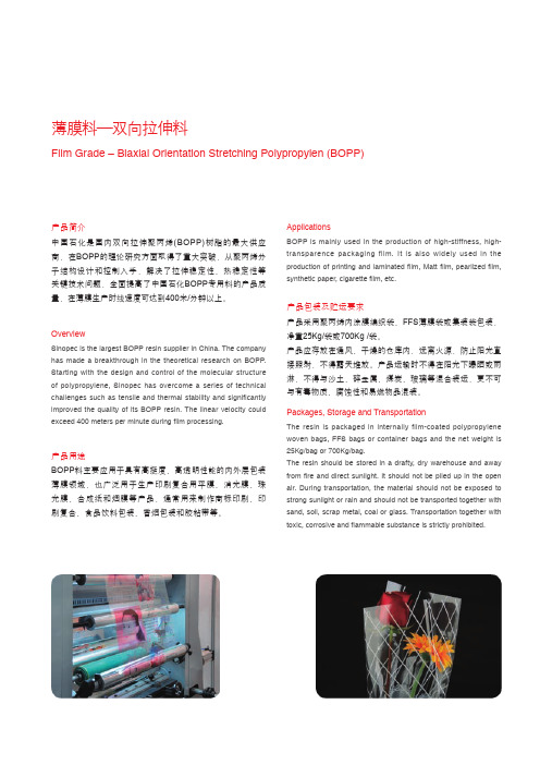
产品简介中国石化是国内双向拉伸聚丙烯(BOPP)树脂的最大供应商,在BOPP 的理论研究方面取得了重大突破,从聚丙烯分子结构设计和控制入手,解决了拉伸稳定性、热稳定性等关键技术问题,全面提高了中国石化BOPP 专用料的产品质量,在薄膜生产时线速度可达到400米/分钟以上。
产品用途BOPP 料主要应用于具有高挺度、高透明性能的内外层包装薄膜领域,也广泛用于生产印刷复合用平膜、消光膜、珠光膜、合成纸和烟膜等产品,通常用来制作商标印刷、印刷复合、食品饮料包装、香烟包装和胶粘带等。
OverviewSinopec is the largest BOPP resin supplier in China. The company has made a breakthrough in the theoretical research on BOPP. Starting with the design and control of the molecular structure of polypropylene, Sinopec has overcome a series of technical challenges such as tensile and thermal stability and signi ficantly improved the quality of its BOPP resin. The linear velocity could exceed 400 meters per minute during film processing.ApplicationsBOPP is mainly used in the production of high-stiffness, high-transparence packaging film. It is also widely used in the production of printing and laminated film, Matt film, pearlized film, synthetic paper, cigarette film, etc.Packages, Storage and TransportationThe resin is packaged in internally film-coated polypropylene woven bags, FFS bags or container bags and the net weight is 25Kg/bag or 700Kg/bag.The resin should be stored in a drafty, dry warehouse and away from fire and direct sunlight. It should not be piled up in the open air. During transportation, the material should not be exposed to strong sunlight or rain and should not be transported together with sand, soil, scrap metal, coal or glass. Transportation together with toxic, corrosive and flammable substance is strictly prohibited.产品包装及贮运要求产品采用聚丙烯内涂膜编织袋、FFS 薄膜袋或集装袋包装,净重25Kg/袋或700Kg /袋。

The science of thin films and coatingsThin films and coatings are an essential part of modern technology that are used in a wide range of applications, from everyday consumer goods to complex scientific instruments. The science of thin films and coatings is a multidisciplinary field that draws upon principles from physics, chemistry, materials science, and engineering. In this article, we will explore the science behind thin films and coatings, their applications, and the challenges associated with their manufacture and characterization.What are thin films and coatings?Thin films are layers of material that are only a few nanometers to several micrometers in thickness. They can be deposited on a substrate through a variety of techniques, including chemical vapor deposition, physical vapor deposition, and electroplating. Coatings are similar to thin films, but they are applied to a surface to provide a functional or decorative layer. Coatings can be applied using techniques such as painting, spraying, or dipping.Thin films and coatings are used in a wide range of applications, including:1. Electronics: Thin films are used to fabricate electronic devices such as transistors, solar cells, and displays.2. Optics: Coatings are used to enhance the performance of optical components such as lenses, mirrors, and filters.3. Biomedical devices: Thin films can be used to improve the biocompatibility and durability of medical implants.4. Energy: Thin films are used in the manufacturing of batteries, fuel cells, and thermoelectric devices.What are the challenges associated with thin film and coating manufacture?Thin film and coating manufacture involves a range of challenges that must be overcome to produce high-quality films. Some of the most significant challenges include:1. Deposition rate: The rate at which the film is deposited can affect the film's properties and quality. Maintaining a consistent deposition rate is essential to producing uniform films.2. Film thickness: Precise control of the film's thickness is critical to achieving the desired performance characteristics. Variations in thickness can lead to changes in the film's optical, mechanical, and electrical properties.3. Adhesion: Coatings must adhere to the substrate to provide effective protection or decoration. Achieving good adhesion requires careful control of the surface preparation and coating process.4. Defects: Films can contain defects such as pinholes, cracks, and impurities that can significantly degrade their performance. Preventing defects requires precise control of the deposition process and the use of high-quality materials.How are thin films and coatings characterized?Characterization of thin films and coatings is essential to understanding their properties and performance. Some of the most common techniques used to characterize thin films and coatings include:1. Scanning electron microscopy: SEM is used to examine the microstructure and morphology of the film.2. X-ray diffraction: X-ray diffraction can be used to determine the crystal structure and orientation of the film.3. Spectroscopic techniques: Spectroscopic techniques such as Fourier transform infrared spectroscopy and Raman spectroscopy can be used to analyze the film's chemical composition and bonding.4. Mechanical testing: The mechanical properties of thin films and coatings, such as hardness and adhesion strength, can be measured using a range of techniques, including nanoindentation, scratch testing, and pull-off testing.ConclusionThin films and coatings are essential components of modern technology, with applications ranging from electronics to energy and biomedical devices. The science behind thin films and coatings is complex, requiring a multidisciplinary approach to achieve high-quality films. The challenges associated with thin film and coating manufacture can be overcome through careful control of the deposition process and material selection. Accurate characterization of thin films and coatings is essential to understanding their properties and performance and ensuring their effective use in a range of applications.。

Fabrication and properties of thinfilmsIntroductionThin films have become an indispensable part of modern technology as they are being used in numerous applications ranging from optical coatings, protective coatings, electronic devices and photovoltaic cells to name a few. Thin films offer unique properties such as improved mechanical, optical, and electrical properties when compared to bulk counterparts. These unique properties make thin films an attractive material for researchers and industry alike.Fabrication TechniquesThin films can be fabricated using a wide range of techniques that include physical vapor deposition (PVD), chemical vapor deposition (CVD), electrochemical deposition (ECD) and sol-gel techniques.Physical vapor deposition (PVD) is a technique that involves the transfer of energy from energetic particles (atoms or molecules) to the surface of the material to produce a thin film. PVD can be carried out using a range of methods, such as sputtering, thermal evaporation, and electron beam deposition.Chemical vapor deposition (CVD) is a technique in which the growth of thin films occurs on a substrate through the chemical reaction of a gas phase precursor. The reaction products deposit on the substrate, forming the desired thin film.Electrochemical deposition (ECD) is a process in which a thin film is grown on a substrate by electrodeposition. The substrate is made the cathode in a bath of a solution that contains the ions of the material to be deposited.Sol-gel process is a chemical method to produce thin films that involves colloidal solutions (sol) that undergo gelation to produce a cross-linked network (gel) of sub-micrometer or nanometer-sized particles.Properties of Thin FilmsThin films have unique properties when compared to bulk materials due to the large surface area to volume ratio. Some of the unique properties of thin films are mentioned below.(a) Mechanical Properties - Thin films possess high strength and hardness when compared to bulk materials due to the reduced grain size and decreased dislocation density.(b) Optical Properties - Thin films possess high transparency or high reflectivity depending on the thickness and the material used for deposition.(c) Electrical Properties - Thin films possess high electrical conductivity, low dielectric constant and capacitive properties when deposited in specific geometries and structures.(d) Magnetic Properties - Thin films possess high susceptibility and susceptibility anisotropy due to the reduced domain size and increased atomic ordering in thin films.Applications of Thin FilmsThin films have become highly essential in various applications spanning across various sectors of technology such as electronic devices, optical coatings, protective coatings, micro-electromechanical systems (MEMS), photovoltaic cells (PV), and biomedical applications.(a) Electronic Devices - Thin films are used extensively in electronic devices such as sensors, electrodes, transistors, capacitors, and memory devices.(b) Optical coatings - Thin films play a vital role in optical coatings such as antireflection coatings, high reflectivity mirrors, and optical filters.(c) Protective coatings - Thin films are used as protective coatings due to their ability to provide high wear resistance, corrosion resistance, and biocompatibility.(d) Photovoltaic cells - Thin films are used in photovoltaic cells for their unique properties such as optical absorption, electrical conductivity, and interface engineering.(e) Biomedical Applications - Thin films are used in biomedical applications such as drug delivery, tissue engineering, and biosensors.ConclusionThin films have revolutionized the field of materials science due to their unique properties and diverse applications. The fabrication of thin films and their properties have been discussed in this article to highlight their importance in various fields of technology. As technology continues to advance, thin films will continue to play a significant role in numerous applications.。
A model to determine the surface hardness of thin films from standardmicro-indentation testsJ.Lesage a,*,A.Pertuz a ,E.S.Puchi-Cabrera b ,D.Chicot aaLaboratoire de Me ´canique de Lille UMR 8107,University of Science and Technology of Lille,BP 179,59653Villeneuve d’Ascq Cedex,FrancebSchool of Metallurgical Engineering and Materials Science,Central University of Venezuela,Apartado Postal 47885,Los Chaguaramos,Caracas 1045,VenezuelaReceived 22March 2005;received in revised form 15September 2005;accepted 30September 2005Available online 21November 2005AbstractThe present investigation has been carried out in order to propose a new model for the determination of the surface hardness of thin films,employing data easily obtained from standard micro-indentation tests.The model is based on the consideration that the substrate has a predominant behavior at the highest indentation loads,whereas at low indentation loads the predominant behavior is that of the film.Such a description is achieved by combining a series and parallel additive laws associated to each behavior,respectively.This approach has been applied for the computation of the hardness of a number of films,including Al 2O 3,Cr,diamond like carbon,Ti,TiC,TiCN,TiN,TiN x and ZrN x ,deposited onto different substrates.It is shown that the results obtained are in good agreement with the predictions provided by other models reported in the literature.D 2005Elsevier B.V .All rights reserved.Keywords:Hardness modeling;Coated systems;Monolayers;Thin films1.IntroductionIn order to improve the resistance to surface damage of materials by mechanical actions,considerable research has been conducted to increase the hardness of the superficial zone of mechanical parts.This is achieved,for example,by physical vapor deposition of hard thin films at their surface.The objective of designing films possessing optimum mechanical properties cannot avoid the determination of their hardness as precisely as possible.Unfortunately,direct measurement of the film hardness,using conventional micro-hardness testers,is not possible for a large range of indentation loads because,for these loads,the substrate undergoes part of the plastic deformation during the indentation process.It is often assumed that this phenomenon,which involves the two materials,begins to be noticeable for loads such that the depth of the indent exceeds one tenth of the film thickness [1,2].In this situation,the hardness number H C ,which is calculatedfrom the measurements,is thus the result of the two,substrate and film,contributions.In order to determine the true hardness of the film it is necessary to separate these contributions.In the past few years,numerous both rational and empirical mathe-matical models were proposed for that purpose on the basis of different assumptions.Whatever the hypotheses,all the models available in literature have in common to suppose a linear additive law for the expression of the composite hardness H C as a function of the film H F and substrate H S hardness:H C ¼H S þa I H F ÀH S ðÞð1Þwhere the coefficient a is associated to the contribution of the film.It is seen that the difference between the models comes only from the expression used to describe the variation of coefficient a as a function of the applied load.One of the earliest works was that of Bu ¨ckle [3],who defined a as a function of a weighting factor associated to the volume of each layer of an influence zone affected by the ter,a more successful model was due to Jo ¨nsson and Hogmark [4],which considered the load supporting areas under the indent associated to the substrate and to the film.From geometrical0040-6090/$-see front matter D 2005Elsevier B.V .All rights reserved.doi:10.1016/j.tsf.2005.09.194*Corresponding author.E-mail address:jacky.lesage@univ-lille1.fr (J.Lesage).Thin Solid Films 497(2006)232–238/locate/tsfconsiderations,these authors expressed the coefficient a in terms of the ratio(t/d)by the following relation:a¼CtdÀC2td2ð2Þwhere C was a constant taking the values0.5or1according to the substrate and film behavior.It was emphasized by the authors that C=1should be taken for low H F/H S when the behavior of the film was supposed to be brittle and C=0.5for high H F/H S for ductile films.The limit between the two behaviors was not given by the authors but we will see thereafter that a value of H F/H S=5seems to be acceptable to guide the choice for C.Considering that this model does not represent the real deformation behavior during indentation,numerous authors have searched to link the coefficient a to the volume of the plastic zones developed under the indent.This was proposed originally by Sargent[5],followed by Burnett and Rickerby [6,7]and Bull and Rickerby[8]who all used a correction factor v called the‘‘interface parameter’’calculated from the following relations:a¼V FVwith V¼V Fþv I V S and vE F I H SE S I H Fqfor H F>H Sð3Þwhere q,and as a consequence v,could be considered as an adjustment parameter.In order to avoid the use of a parameter such as v,Chicot and Lesage[9]in1995proposed a model based on the superposition of two hypothetic systems representing the volumes of the plastic deformation in the film and in the substrate under the indent.The mathematical development led to the following expression for a:a¼32tdk I tg nðÞ1=3H FE F1=2þH SE S1=2"#À2td3k I tg nðÞH FE F3=2þH SE S3=2"#ð4Þfor which it is seen that the second term becomes negligible when the diagonal length d is higher than that of the thickness t,then:a¼32tdk I tg nðÞ1=3H FE F1=2þH SE S1=2"#ð5ÞIn the two cases,provided that E F and E S are known,the determination of H F is possible,using a simple routine program applied to each couple of values t and d.Basing their reasoning on the former model put forward by Burnett and Rickerby [6,7],Ichimura et al.[10]have recently proposed an expression for the coefficient a which is very similar to that given in Eq.(5),if the term associated to the substrate is disregarded:a¼3t tg nðÞ1=3H FF1=2ð6ÞAnother way to consider the problem was that proposed by Korsunsky et al.[11]who have recently developed a model based on the work of indentation associated to the deformation energy of the two materials and their interface under the indent. From these considerations they obtained the following expres-sion for a:a¼11þk K I b2ð7Þwhere b is the relative indentation depth d/7t.H F is determined by fitting the experimental values of H C in terms of b.J.Lesage et al./Thin Solid Films497(2006)232–238233On the basis of geometrical considerations about the dimension of the indent,very recently,Puchi-Cabrera [12]has proposed the computation of the composite hardness using the following expression (8),where the two constants (k P and n P )represent the material parameters:a ¼exp Àk P I b n P ðÞð8ÞSome of the models listed above require the knowledge or the choice of data that have to be deduced from other experiments or literature.Some others,which need a fitting method to describe the variations of H C with the load,fail to predict the hardness of the film when the number of experiments is too poor,in particular for low indentation loads.The objective of the present work is to propose a model which avoids the knowledge or choice of any other data (Young modulus of the film in particular)than that obtained easily from standard measurements (e.g.thickness and apparent hardness).The basic idea on which we will now build this model found its origin in the analogy between the variation of the Young modulus of reinforced composites with the volume fraction of particles,and the variation of the composite hardness with the indentation load.The global behaviorTable 1Indent diagonal (d )and related composite hardness (H C )for different film and substrate systems (Jo¨nsson and Hogmark [4],Burnett and Rickerby [6,7],Chicot and Lesage [9],Puchi-Cabrera [12],Puchi-Cabrera et al.[13],Ahn and Kwon [14]and Lesage et al.[15])No.Film/t (in A m)Indent diagonal,d (in A m)and composite hardness,H C (in GPa)Ref.Substrate,H S /E S (H S and E S in GPa)1Cr/1.0d 3.0 4.47.210.415.623.028.8[4]BBS,6.7/200H C 10.39.68.98.67.67.0 6.72Cr/1.0d 4.47.911.817.425.332.4HSLA steel,5.0/200H C 9.67.4 6.7 6.1 5.8 5.33Cr/1.0d 4.3 6.912.018.728.441.552.7SS,1.9/200H C 5.0 3.9 3.2 2.7 2.3 2.2 2.04Cr/1.0d 5.69.617.626.739.358.073.9Copper,0.9/200H C 3.0 2.0 1.5 1.3 1.2 1.1 1.05TiN/2.5d 6.29.815.122.928.737.754.3[6,7]Tool steel,6.0/200H C 12.19.78.17.1 6.8 6.5 6.36TiN/9.0d 6.210.216.822.431.648.1Tool steel,6.0/200H C 24.117.813.111.19.38.07TiN/2.0d 5.110.518.228.443.554.5Stainless,6/200H C 7.1 4.2 2.8 2.3 2.0 1.98TiN/5.5d 6.111.020.536.048.8Stainless,1.6/200H C 12.57.7 4.4 2.9 2.39Ti /4.0d 6.411.417.526.739.449.565.193.6[9]High C steel,2.0/200H C 4.5 3.6 3.0 2.6 2.4 2.3 2.2 2.110TiC/4.0d 7.311.617.922.730.745.9High C steel,6.4/200H C 17.413.811.610.89.88.811ZrN 0.5/3.0d 2.9 4.48.615.423.633.649.7[12]Steel,1.6/220H C 10.99.5 6.1 3.8 3.3 3.2 2.912ZrN 0.6/3.0d 2.2 3.87.714.221.633.750.0Steel,1.6/220H C 18.412.77.6 4.5 3.9 3.2 2.913ZrN 0.7/3.0d 1.7 3.1 6.011.519.631.650.0Steel,1.6/220H C 29.819.112.6 6.9 4.7 3.6 2.914TiN 0.55/3.0d 2.5 4.29.416233551[13]316L,2.7/200H C 14.810.5 5.2 3.6 3.5 3.0 2.915TiN 0.65/3.0d 2.2 3.47.314233351316L,2.7/200H C 19.216.08.7 4.7 3.5 3.4 2.916TiN 0.75/3.0d 1.6 2.6 5.914223349316L,2.7/200H C 36.227.413.3 4.7 3.8 3.4 3.117Al 2O 3/1.8d 1.7 2.1 2.5 2.8 3.1 3.4 3.6 4.6 5.4 6.1[14]Glass,6.6/75H C 10.510.210.110.19.99.99.89.48.98.718Al 2O 3/1.0d 1.7 2.6 3.9 4.8 5.8 6.4Glass,6.6/75H C 10.39.68.88.37.97.719Al 2O 3/1.9d 1.6 2.0 2.3 2.6 2.9 3.2 3.5 4.7 5.9 6.8Glass,4.2/220H C 10.610.210.19.79.38.98.8 6.7 5.6 5.220TiN/3.25d 4.57.07.810.712.817.022.025.029.732.435.5[15]M-2steel,8.6/200H C 22.918.918.316.215.312.811.511.410.510.310.121TiCN/3.25d 3.4 5.2 6.610.111.716.722.129.8M-2steel,8.5/200H C 40.134.325.518.218.313.311.410.422TiN/1.4d 7.613.824.036.947.361.990.1131–Low C steel,1.8/200H C 8.0 4.9 3.2 2.7 2.5 2.4 2.3 2.223DLC/1.6d 14.723.737.546.061.289.3137Low C steel,1.9/200H C4.33.32.82.62.52.32.0J.Lesage et al./Thin Solid Films 497(2006)232–238234exhibits similar features since the apparent Young modulus or the hardness tends to two distinct limits:the matrix and the reinforcement material elastic modulus on one hand,and the substrate and film hardness on the other hand.Although it is clear that there is no relation between the elastic deformation of composites and the elasto-plastic deformation of the film and the substrate during indentation,the mathematics used to describe the variations can be considered in a similar way.In order to discuss the validity of the new model,the calculated hardness of various films on several substrates will be compared to the predictions given by a set of representative models applied to experimental values coming either from our laboratory or from literature.2.Hardness measurements and data collectionThe films tested in our laboratory were prepared by an industrial vapor deposition process.Two types of films were deposited on a low carbon steel after careful polishing:TiN and diamond like carbon(DLC)films of thickness of1.4and1.6 A m,respectively.Vickers indentations were then performed on the as-deposited samples using a Leco micro-hardness tester with loads ranging from0.25to20N.Five tests were performed at each load level in order to get a reasonable confidence in the calculated average hardness value.The thickness of the film was measured directly either by microscopy on a cross-section of a coated sample or using the ball cratering technique.Another set of data was collected from the literature,for films produced by different physical and chemical vapor deposition techniques on various steel sub-strates.Table1summarizes all the bibliographical data associated to the different film and substrate systems and collects the measured diagonal of the indent and the corresponding composite hardness.The thickness(t)and indent diagonal(d)are both expressed in micrometer,whereas hardness(H S,H C)and Young modulus(E S)are given in gigapascal.3.The modelMost of the models available in the literature express the composite hardness H C as a linear additive law in terms of the film(H F)and substrate(H S)hardness(Eq.(1)).This expression will be called a‘‘series relation’’in the following. On the other hand,no model of the type:1 H C ¼1H Sþa1H FÀ1H S;ð9Þwhich could be called a‘‘parallel relation’’,has been tried. However,similar relations deduced from very simple rheologic models have been used to represent the upper and lower bounds within which the elastic modulus of reinforced composites,as a function of the volume fraction of particles, lies[16].Depending on this fraction,the modulus of the composite tends towards one bound or the other.Therefore,a model for the Young modulus as a function of the volume fraction of particles could be a combination of these two relations in order to allow the transition from a matrix tendency behavior to a reinforcement material tendency behavior.We will examine how this very simple idea could be transposed to the composite hardness of thin films.Let us consider first a typical variation of the composite hardness as a function of the ratio of the film thickness to the diagonal of the indent(t/d),as shown in Fig.1.It is observed that the variation of t/d ranges from0to a value near1,as the substrate becomes involved in the indentation process.This value of1comes from the‘‘rule of the tenth’’observed by numerous authors like Bu¨ckle[3].It has been observed an influence of the substrate when the ratio between the Vickers indentation depth and the film thickness, D/t,is equal to,since D is equal to d/7,then d/t=0.7,near1, which can be considered as a conservative limit in order to simplify the calculation.In addition,a value very close to1has been observed for a large variety of films and substrates.For higher indentation loads,d is high,then t/d tends to0 and the composite hardness tends to that of the substrate(i.e.to the lower bound).On the contrary,when the indentation loads are lower,the composite hardness tends to that of the film and consequently,t/d tends to1(i.e.to the upper bound).If we consider the analogy with the elastic modulus of reinforced composites for which:E U¼E MþV R I E RÀE MðÞUpper boundðÞð10Þ1E L¼1E MþV R I1E RÀ1E MLower boundðÞð11Þwe may write the following relations for the upper(H CU)and lower bound(H CL)of the composite hardness,where the coefficient a is expressed here as a function of t/d:H CU¼H SþftdI H FÀH SðÞð12ÞCompositehardness(GPa)Thickness on diagonal ratio (t/d)Fig.1.Typical variation of the composite hardness,H C,as a function of the ratio between the film thickness and indent diagonal,t/d(TiN film on M-2 steel,t=3.25A m[15]).1H CL¼1H SþftdI1H FÀ1H Sð13ÞJ.Lesage et al./Thin Solid Films497(2006)232–238235The first one corresponds to the film tendency behavior for lower t /d and the second one to the substrate tendency behavior for higher t /d .In order to allow the transition between substrate and film tendency we consider the following expression,which combines the two previous relations:H C ¼H CL þf t dI H CU ÀH CL ðÞð14ÞThe transition between H CL and H CU depends on the variation of t /d between 0and 1.Therefore,the problem is to find a form as simple as possible for the function f (t /d ).A first approach is to consider the relation known as Meyer’s law [17],which expresses the variation of the size of the indent d as a function of the applied load P :P ¼a m I d n mð15Þwhere n m is called the Meyer index.This relation is traditionally used for a single material.Applied to the particular case of a film substrate couple (Fig.2),we showed that the evolution of the measured diagonal and the applied load,linear in bilogarithmic coordinates,can also be expressed by a similar relation:P ¼a 4I d n4ð18ÞUsing the standard Vickers hardness number,it is possible to write the composite hardness:H C ¼a IP d 2¼a I a 4I d n 4À2ð19ÞAnd by introducing the thickness of the film t in relation (19)H C ¼a V t d 2Àn 4;with a V ¼a I a 4=t 2Àn 4ð20ÞIn this relation,factor n *,as it is for Meyer index n m ,characterizes the way in which the hardness varies with load.In order to study the composite hardness,the choice for a f (t /d )relation should then involve that factor.In addition,the function should admit the same limits than t /d (0and 1)and should tend asymptotically to 0for the highest loads.Such a function couldbe for example the following which has the advantage of being very simple:Ft d ¼t d m¼f ;where m ¼1=n 4ð21ÞIn these conditions the composite hardness can be expressed by the general relation:H C ¼1Àf ðÞ=1=H S þf I 1H F À1H Sþf I H S þf I H F ÀH S ðÞðÞð22ÞRewriting this relation as a polynomial in terms of H F allows thecalculation of the film hardness which is thus the positive root of the equation:A P I H 2F þB P I H F þC P ¼0;withfA P ¼f 2I f À1ðÞB P ¼À2f 3þ2f 2À1ðÞI H S þ1Àf ðÞI H CC P ¼f H C H S þf 2I f À1ðÞI H 2Sð23ÞThe value of m is obtained directly by a linear regression performed on all the experimental points for a given film substrate couple (see Fig.2):ln d ¼m I ln P þbð24Þ4.Application and validation of the modelWe have just seen that m is easily obtained as a first step.The second step is to calculate H F for each H C from relation (23).The values obtained for H F are not constant;they vary as a function of d .Some typical variations are presented in Fig.3for several films.It is seen that the lines ln H F –ln d could be ascending,descending or exhibit a change of slope.Whatever the model,Jo ¨nsson,Chicot-Lesage,Ichimura et al.or the present model,the variations are similar although the ampli-tudes are different.Due to this similarity and since the models are based on very different assumptions,the variations should be related to physical phenomena instead of being related to the model.Even if these phenomena are not completely known,one can cite some of them such as the indentation size effect [18–21],the cracking in the neighborhood of the indent [22],the elastic contribution of the substrate for the lowest loads [23],or the crushing of the film for the highest loads [24](values of H C <1.1H S are not considered here).Direct comparison of the models could not be done easily under the form of relations deduced from Fig.3.Furthermore,these relations could not be compared with the sole extrapo-lated values given by the models of Puchi and Korsunsky et al.,which are supposed to correspond to the moment when the substrate ceased to participate in the indentation process.As mentioned above,we may consider that this limit of substrate influence corresponds to t /d =1.That is why we will now calculate H F for this ratio in order to make useful comparisons.l n d (d i n µm )ln P (P in N)Fig.2.Example of the relation between indent diagonal,d ,and applied load,P ,in bilogarithmic coordinates (TiN film on M-2steel,t =3.25A m [15]).J.Lesage et al./Thin Solid Films 497(2006)232–238236Table 2summarizes all the results obtained for the following models:Jo ¨nsson–Hogmark,with the condition H F /H S <or >5for the choice of C ,Chicot-Lesage,Ichimura et al.,Korsunsky et al.,Puchi-Cabrera and the new model.The model of Bull was not considered here since the similar model of Ichimura et al.is easier to apply.In order to validate the new model,we compare its predictions to the average predictions of all the other modelsTable 2Results of the application of the five models analyzed in the present work:Jo ¨nsson and Hogmark [4],Chicot and Lesage [9],Ichimura et al.[10],Korsusnky et al.[11]and Puchi-Cabrera [12]Ref.No.Film Jo ¨nsson and Hogmark Chicot and Lesage Ichimura et al.Korsunsky et al.Puchi-Cabrera H F (GPa)H F (GPa)E F (GPa)Average New model [4]128010.411.312.710.611.110.8T 0.411.8228017.119.621.111.316.417.7T 1.428.9328013.312.512.8 5.611.912.6T 0.511.3428012.212.412.5 3.812.712.4T 0.212.3[6,7]560019.625.029.515.817.020.5T 3.329.5660019.721.123.728.948.721.5T 1.721.2760022.222.322.99.611.122.5T 0.322.9860018.818.918.817.224.318.4T 0.719.1[9]9120 5.57.0 6.8 5.17.3 6.4T 0.77.11046019.521.323.718.844.720.8T 1.922.8[12]1146014.514.614.211.716.914.4T 0.211.51246018.918.317.320.737.318.8T 1.214.51346026.124.821.233.252.226.3T 4.420.2[13]1460015.515.416.319.831.316.7T 1.815.11560020.519.720.222.729.020.8T 1.119.31660027.827.328.143.365.031.6T 6.730.0[14]1715010.410.310.310.710.610.5T 0.210.61815010.810.410.811.111.610.9T 0.411.61915010.410.610.412.611.310.7T 0.410.4[15]2030023.923.523.025.129.323.9T 0.825.32125557.339.939.051.568.849.6T 7.246.5–2260022.621.322.0 5.414.920.2T 3.121.82344028.027.027.89.58.727.6T 0.429.2The calculated averages do not include the hardness values printed in italics in the table.The predicted values according to the new model are also shown for comparison.d (µm)H F (G P a )a) Sample n ° 1.H F (G P a )d (µm)b) Sample n ° 9.H F (G P a )d (µm)c) Sample n ° 10.H F (G P a )d (µm)d) Sample n ° 23.Fig.3.Influence of the applied load on the film parison of the models.J.Lesage et al./Thin Solid Films 497(2006)232–238237for each film.If the standard errors on this average are examined,we note that for some models the predictions (in italic in Table 2)differ from the average for more than one standard error.For this reason they were not taken into account for the calculation of the average hardness which appears in Table 2.Observation of Table 2confirms that the limit of 5for H F /H S for the choice of constant C in the Jo ¨nsson–Hogmark model is pertinent since the predictions are well in accordance with the average hardness.It is also the case for the predictions of the present model,which are presented in Fig.4.5.ConclusionsWe have shown in this paper that,starting from an analogy with reinforced composites,it is possible to represent the behavior of a film–substrate couple under indentation,from the higher loads,when the couple tends to behave like the substrate,to the lower loads,when it tends to behave like the film.The new model proposes to combine these two tendencies according to the apparent Meyer’s law,which describes how the apparent composite hardness varies as a function of the applied load.The predictions for the film hardness,calculated using this model,are of the same order than those obtained with more complicated or delicate models proposed in literature.Another interesting feature of this model is that it applies well even when the number of available data is small,contrary to other models which need a fitting method to derive the film hardness.The hardness of a material,as deduced from indentation tests,is definitely not an intrinsic property such as its elastic modulus or its melting temperature.The hardness number is in fact a representation of the resistance to indentation of a material under a given load and a given indenter.As a consequence,it is not possible to state that one model shouldgive more accurate values for H F than another one.As it was shown here,though,the calculated H F ,at least for H F values extrapolated for t =d ,are sufficiently close to allow a certain confidence in the predictions.The recent developments of depth sensing indentation equipment [25],since they permit the direct determination of the elastic modulus [26]and of the elasto-plastic laws [27],will be of extreme importance to answer the following question:Is it possible to express the hardness in terms of an intrinsic property of a material?References[1]Y .Sun,S.Zheng,T.Bell,Thin Solid Films 258(1995)198.[2]X.Cai,H.Bangert,Thin Solid Films 264(1995)59.[3]H.Bu ¨ckle,in:J.W.Westbrook,H.Conrad (Eds.),The Science ofHardness Testing and its Research Applications,American Society for Materials,Metals Park,OH,1973,p.453.[4]B.Jo ¨nsson,S.Hogmark,Thin Solid Films 114(1984)257.[5]P.M.Sargent,Ph.D.Thesis,University of Cambridge,United Kingdom,1979.[6]P.J.Burnett,D.S.Rickerby,Thin Solid Films 148(1987)41.[7]P.J.Burnett,D.S.Rickerby,Thin Solid Films 148(1987)51.[8]S.J.Bull,D.S.Rickerby,Surf.Coat.Technol.42(1990)149.[9]D.Chicot,J.Lesage,Thin Solid films 254(1995)123.[10]H.Ichimura,F.M.Rodriguez,A.Rodrigo,Surf.Coat.Technol.127(2000)138.[11]A.M.Korsunsky,M.R.McGurk,S.J.Bull,T.F.Page,Surf.Coat.Technol.99(1998)171.[12]E.S.Puchi-Cabrera,Surf.Coat.Technol.160(2002)177.[13]E.S.Puchi-Cabrera,J.A.Berrios,D.G.Teer,Surf.Coat.Technol.157(2002)185.[14]J.H.Ahn,D.Kwon,Mater.Sci.Eng.,A Struct.Mater.:Prop.Microstruct.Process.285(2000)172.[15]J.Lesage, D.Chicot, A.M.Korsunsky,J.Tuck, D.G.Bhat.14thInternational Conference on Surface Modification Technologies,Paris,France,September 11–132000,Surface Modification Technologies XIV ,Edited by T.S.Sudarshan and M.Jeandin,ASM International,Materials Park,Ohio and IOM Communications Ltd.,UK,2001,117.[16]W.D.Callister Jr.,Materials Science and Engineering,an Introduction,Fifth edition,John Wiley &Sons,NewYork NY ,1999,p.523.[17]E.Meyer,Z.Ver.Dtsch.Ing.52(1908)645.[18]J.Gong,Z.Zhao,Z.Guan,H.Miao,J.Eur.Ceram.Soc.20(2000)1895.[19]K.Sangwal,B.Surowska,P.Blaziak,Mater.Chem.Phys.77(2003)511.[20]K.Sangwal,B.Surowska,P.Blaziak,Mater.Chem.Phys.80(2003)428.[21]J.G.Swadener,E.P.George,G.M.Pharr,J.Mech.Phys.Solids 50(2002)681.[22]J.R.Tuck,A.M.Korsunsky,R.I.Davidson,S.J.Bull,D.M.Elliott,Surf.Coat.Technol.127(2000)1.[23]J.Musil,F.Kunc,H.Zeman,H.Polakova,Surf.Coat.Technol.154(2002)304.[24]Y .Fu,X.Zhu,K.Xu,J.He,J.Mater.Proc.Technol.83(1998)209.[25]W.C.Oliver,G.M.Pharr,J.Mater.Res.7(1992)1564.[26]N.X.Randall,A.Harris,Wear 245(2000)196.[27]A.E.Giannakopoulos,S.Suresh,Scr.Mater.40(1999)1191.H F n e w m o d e l (G P a )HF mean (GPa)parison between the predictions of the new model and the average of the predictions of other models.J.Lesage et al./Thin Solid Films 497(2006)232–238238。
The Chemistry and Physics of ThinFilmsThin films are a fascinating topic for researchers in the fields of chemistry and physics. These films, which are only a few nanometers thick, have unique properties and behavior that make them important in various applications, from electronics to medicine. In this article, we will explore the chemistry and physics behind thin films, their properties and applications, and the methods used to create and study them.Chemistry of Thin FilmsThe chemistry of thin films is complex and depends on the material used and the deposition technique employed. Thin films can be made from a variety of materials, including metals, semiconductors, oxides, polymers, and glasses. The choice of material depends on the desired properties of the film, such as its electrical conductivity, optical properties, or mechanical strength.The deposition technique used to create thin films can also affect its chemistry. The most common method for creating thin films is by physical vapor deposition (PVD) or chemical vapor deposition (CVD). In PVD, the material is vaporized in a vacuum chamber and deposited onto a substrate, forming a thin film. In CVD, a gas is used to react with the substrate, forming a thin film. Depending on the material and the deposition technique used, the chemistry of the thin film can vary widely.Physics of Thin FilmsThin films exhibit unique physical properties due to their thickness. For example, thin films may have different optical properties than their bulk counterparts due to changes in their refractive index or absorption properties. Additionally, thin films may exhibit different electronic conductivities or mechanical properties compared to the bulk material.The physics of thin films is also influenced by the deposition method and the substrate. For example, thin films deposited on a flexible substrate may exhibit different mechanical properties than films deposited on a rigid substrate. Similarly, the orientation of the crystal structure in thin films can be influenced by the substrate on which they are deposited.Properties and Applications of Thin FilmsThin films have a variety of unique properties that make them useful in many applications. For example, thin films can be used as thin-film transistors in electronic devices, where the film acts as the semiconductor layer. Thin films can also be used as anti-reflection coatings on optics or as transparent conductive coatings.In addition, thin films can be used in medical applications, such as drug delivery systems or biosensors. Thin films can also be used as coatings on mechanical components to improve their wear resistance or lubrication properties. Furthermore, thin films can be employed as gas sensors in environmental monitoring or as catalysts in chemical reactions.Methods for Studying Thin FilmsThere are a variety of methods used to study thin films, including electron microscopy, X-ray diffraction, and spectroscopy. Electron microscopy can be used to visualize the morphology of thin films, while X-ray diffraction can be used to identify the crystal structure of the film. Spectroscopy techniques, such as UV-Vis spectroscopy or infrared spectroscopy, can be used to study the electronic and optical properties of thin films.ConclusionThin films are an exciting area of research for chemists and physicists. The chemistry and physics of thin films are complex and depend on the material used and the deposition technique employed. Thin films have unique properties and behavior that make them important in various applications, from electronics to medicine. Finally, a variety oftechniques exist for studying thin films, allowing researchers to gain insight into their properties and behavior.。
Surface Roughness and Adhesion of ThinFilmsThin films, which have thicknesses in the range of billionths to microns, are often applied in industry and research to achieve specific physical, chemical, optical or electronic properties. Surface roughness and adhesion are two important factors that affect the performance and quality of thin films. In this article, we will discuss the relationship between surface roughness and adhesion of thin films, the impact of different deposition processes on surface roughness, and tools used to measure surface roughness and adhesion.Relationship Between Surface Roughness and AdhesionThe surface roughness of a thin film refers to the irregularity or variability on the surface due to manufacturing processes or environmental effects. The adhesion of a thin film, on the other hand, refers to how well the film sticks to the substrate or to other layers. In general, the surface roughness of a thin film can affect its adhesion in several ways.Firstly, the surface roughness can affect the contact area between the thin film and the substrate. As the roughness increases, the actual contact area decreases, resulting in reduced adhesion. Secondly, the roughness can increase the interfacial energy between the thin film and the substrate, making it easier for the film to buckle or delaminate. Thirdly, the roughness can introduce stresses and defects in the thin film, which can cause cracks, wrinkles or adhesion failures.Therefore, it is important to control the surface roughness of thin films to improve their adhesion and durability. This can be achieved by optimizing the deposition parameters, such as temperature, pressure, gas flow and substrate treatment, as well as by using appropriate surface coatings or adhesion promoters.Impact of Different Deposition Processes on Surface RoughnessThe surface roughness of a thin film can be influenced by the deposition process itself. Some common deposition techniques for thin films include:- PVD (Physical Vapor Deposition) - which involves heating a material in a vacuum chamber until it evaporates and condenses onto a substrate. PVD can produce smooth and uniform films with low roughness, but it may also cause surface defects due to ion bombardment or incomplete coverage.- CVD (Chemical Vapor Deposition) - which involves introducing a reactive gas to a substrate and causing a chemical reaction that forms a thin film. CVD can produce conformal and dense films with low roughness, but it may also lead to roughness variations due to the concentration gradients or particle size effects.- ALD (Atomic Layer Deposition) - which involves alternating the exposure of a substrate to two or more precursors, resulting in the growth of an atomically thin film. ALD can produce highly homogeneous and defect-free films with low roughness, but it may also require longer processing times and higher costs.In addition to the deposition process, the surface roughness of a thin film can also be affected by the substrate material, the film thickness, the annealing process, and the exposure to humidity or chemicals. Therefore, it is essential to characterize the surface roughness of thin films using appropriate tools and methods.Tools Used to Measure Surface Roughness and AdhesionThere are various techniques available to measure the surface roughness and adhesion of thin films. Some of the commonly used tools include:- Atomic force microscopy (AFM) - which uses a scanning probe to measure the topography and roughness of a surface with nanometer resolution. AFM can also be used to detect defects or impurities in the film, and to probe the adhesion force between the film and the substrate.- X-ray reflectivity (XRR) - which uses an X-ray beam to measure the density and thickness of a film, as well as the interfaces and multilayer structures. XRR can also be used to estimate the surface roughness and the crystallographic orientation of the film.- Contact angle measurement (CAM) - which uses a liquid droplet to measure the wettability and adhesion of a surface. CAM can be used to quantify the surface energy and hydrophobicity of the film, as well as to identify the presence of contaminants or functional groups.- Scratch testing - which uses a stylus or a blade to scratch the surface of a film and measure the critical load or the failure mode. Scratch testing can be used to evaluate the adhesion strength, the frictional properties, and the wear resistance of the film.ConclusionIn summary, the surface roughness and adhesion of thin films are crucial parameters that affect their performance and stability. The relationship between surface roughness and adhesion can be complex, and can depend on various factors such as deposition process, substrate material and post-processing conditions. Therefore, it is important to carefully control and measure the surface roughness and adhesion of thin films using appropriate tools and methodologies. By doing so, we can optimize the design and functionality of thin films for a wide range of applications in electronics, optics, energy, biomedical engineering and more.。
Overview and Challenges of Thin Film Solar Electric Technologies H.S. UllalPresented at the World Renewable Energy Congress X and Exhibition 2008Glasgow, Scotland, United KingdomJuly 19–25, 2008 Conference Paper NREL/CP-520-43355 December 2008NOTICEThe submitted manuscript has been offered by an employee of the Alliance for Sustainable Energy, LLC (ASE), a contractor of the US Government under Contract No. DE-AC36-08-GO28308. Accordingly, the US Government and ASE retain a nonexclusive royalty-free license to publish or reproduce the published form of this contribution, or allow others to do so, for US Government purposes.This report was prepared as an account of work sponsored by an agency of the United States government. Neither the United States government nor any agency thereof, nor any of their employees, makes any warranty, express or implied, or assumes any legal liability or responsibility for the accuracy, completeness, or usefulness of any information, apparatus, product, or process disclosed, or represents that its use would not infringe privately owned rights. Reference herein to any specific commercial product, process, or service by trade name, trademark, manufacturer, or otherwise does not necessarily constitute or imply its endorsement, recommendation, or favoring by the United States government or any agency thereof. The views and opinions of authors expressed herein do not necessarily state or reflect those of the United States government or any agency thereof.Available electronically at /bridgeAvailable for a processing fee to U.S. Department of Energyand its contractors, in paper, from:U.S. Department of EnergyOffice of Scientific and Technical InformationP.O. Box 62Oak Ridge, TN 37831-0062phone: 865.576.8401fax: 865.576.5728email: mailto:reports@Available for sale to the public, in paper, from:U.S. Department of CommerceNational Technical Information Service5285 Port Royal RoadSpringfield, VA 22161phone: 800.553.6847fax: 703.605.6900email: orders@online ordering: /ordering.htmPrinted on paper containing at least 50% wastepaper, including 20% postconsumer wasteOverview and Challenges of Thin Film Solar Electric Technologies*Harin S. Ullal, Ph.D.National Center for PhotovoltaicsNational Renewable Energy Laboratory1617 Cole BoulevardGolden, Colorado 80401 USATel: 303-384 6486, Fax: 303-384 6430, E-mail: harin_ullal@1 IntroductionIn this paper, we report on the significant progress made worldwide by thin-film solar cells, namely, amorphous silicon (a-Si), cadmium telluride (CdTe), and copper indium gallium diselenide (CIGS). Thin-film PV technology status is also discussed in details. In addition, R&D and technology challenges in all three areas are elucidated in this paper. The worldwide estimated projection for thin-film PV technology production capacity announcements are estimated at more than 5000 MW by 2010.2 Thin-Film Amorphous SiliconSolar Cell TechnologiesAmorphous (a-Si) solar cells were fabricated at RCA laboratory in 1976. The initial conversion efficiency was 2.7%. Since then, considerable progress has been made to improve the stabilized total-area, conversion efficiency of a-Si in the range of 12% to 13% for small-area laboratory solar cells. This section describes the family of a-Si solar cells that include microcrystalline, nanocrystalline and micromorph solar cells. a-Si solar cells can be either a single junction, dual junction or multijunction devices. The highest total-area, stabilized efficiency of 12% to13% has been demonstrated using tandem and multijunction devices.a-Si solar cells are fabricated on substrates such as low-cost, sodalime glass, stainless steel and polyimide. All manufacturing plants use the plasma-enhanced chemical vapor deposition (PECVD) for the deposition process. The typical superstrate structure is p-i-n on glass or substrate structure of n-i-p on foil with a TCO as a top contact and Al along with ZnO as the bottom contact. The ZnO/Al serves as a back reflector to enhance the short-circuit current (Jsc) by approximately 15%. Ag has been tried as a back metal contact instead of Al, but has been found to be problematic in terms of product reliability in module fabrication. However, with the recent developments in the tandem (micromorph) devices, the performance of ZnO/Ag or ZnO/Ag/Al have been quite reliable for stable back contacts.Although much of the a-Si commercial production has been single junction modules fabricated on low-cost, sodalime glass and multijunction devices on stainless steel substrates, there is a great deal of effort worldwide to introduce tandem devices using a-Si as the top cell and microcystalline absorbers as the bottom cells. This is also sometimes referred to as micromorph devices. The typical intrinsic layer thickness in a single junction device is about 0.3 micrometer, since this has demonstrated the best stabalized device efficiency [2]. In the case of multijunction devices, the total thickness of the 3 devices is about 0.7 micrometer. This poses a major challenge for the micromorph tandem device, since the typical thickness is about 2.0 mircometer for the bottom cell and it is an indirect semiconductor. This needs higher thicknesses to absorb the photons in the solar spectrum. Thus some of the major challenge for scientists is to develop i) higher efficiency solar cells, ii) reduce the light induce changes in the devices, iii) develop higher deposition rates for the––––––––––––––––––––––––––––––––* Employees of the Midwest Research Institute under Contract No. DE-AC36-99GO10337 with the U.S. Dept. of Energy have authored this work. The United States Government retains and the publisher, by accepting the article for publication, acknowledges that the United States Government retains a non-exclusive, paid-up, irrevocable, worldwide license to publish or reproduce the published form of this work, or allow others to do so, for United States Government purposes.microcrystalline bottom cell without compromising on the opto-electronic properties ofthe a-Si tandem devices, which could potentiallyhave detrimental effect on the solar cell performance, and iv) reduce the manufacturingcost of the a-Si power modules.The market share for a-Si modules is several percent of the worldwide PV sales. The majorplayers are Uni-Solar, USA, Energy Photovoltaics(EPV), USA, Power Film Solar, USA, OptiSolar ,USA, Kaneka, Japan, Mitsubishi, Japan, SharpSolar, Japan, Schott Solar, Germany and many more. There are also five equipment suppliers forturnkey a-Si factories, namely, Applied Materials,USA, Anwell Technologies, Singapore, Hind High Vac, India, Oerlikon Solar, Switzerland, andUlvac, Japan. Most recently, Applied Material,USA announced the sale of a turnkey manufacturing plant worth $ 1.9 Billion, presumably to the LDK Investor Group in China.This potentially could translate to a productioncapacity of 1000 MW per year of a-Si powermodules. The new company is called Best Solarand is based in China.3 Thin-Film Cadmium TellurideSolar Cell TechnologiesThin-film CdTe solar cells are one of the mostpromising thin-film PV devices. With a bandgapof 1.45 eV it has an excellent match with the solarspectrum. Since these are direct bangap semiconductors with high absorption coefficient,very thin absorber layer are needed to absorb thephotons. Theoretical efficiencies for these devicesare about 26%. Laboratory efficiencies of 16.5%for thin-film CdTe solar cell has been demonstrated by NREL scientists [3]. Historically,thin-film CdTe solar cells were referred to as the“dark horse” for thin-film PV devices. Subsequentconcerted research effort by several groups worldwide has resulted in developing several deposition processes for the growth of the absorber layer. The processes are close-space sublimation, electrodeposition, vapor transport deposition, spray, screen-printing, sputtering, physical vapor deposition, laser ablation, metalorganic chemical vapor deposition, molecular beam epitaxy, and atomic layer epitaxy [4]. Many of these processes has resulted in thin-film CdTe solar efficiency of 10% or higher. Five of these processes have demonstrated prototype powermodules, namely, close-space sublimation, electrodeposition, spray, screen printing and vapor transport deposition.For thin film CdTe technology, five key research, development, and technology challenges include: (1) standardization of equipment for deposition ofthe absorber layer, (2) higher module conversion efficiency, (3) back-contact stability, (4) reduced absorber layer thickness to less than 1 micrometer and (5) control of film and junction uniformity over large area for power modules. The current status of the manufacturing technology is power modules with a conversionefficiency of 10.5% made by First Solar (FS). Their manufacturing cost is $ 1.14 per watt and installed system price is in the range of $ 4-5 per watt, the lowest in the industry for any PV system.Clearly, FS is the world leader in all thin-film PV manufacturing technology. They have an installed capacity of more than 132-MW in Perrysburg, Ohio. They have also installed a 176-MW manufacturing plant in Germany in 2007. In addition, they are installing a 704-MW thin-film CdTe manufacturing line in Malaysia, which will be commissioned in phases in 2009. Thus FS’s target is to have a worldwide installed manufacturing capacity of 1000-MW by December 2009. To date, FS has sold a few 100 MW of thin-film CdTe power modules to sixinstallers in Germany for commercial roof-top and utility-scale applications. They are also working very closely with a system integrator -- Juwi Solar to install a 40-MW solar farm in Saxony, Germany to be completed in December 2008.Like for all PV companies, the German feed-in-tariff law has clearly helped in the market acceptance of the thin-film CdTe power modules. A few more emerging companies are AVA Solar, Colorado, USA, Primestar Solar, Colorado, USA, Calyxo, Ohio, USA, Calyxo, Germany, and Avendi, Italy.4 Thin-Film Copper Indium GalliumDiselenide Solar Cell Technologies Thin-film PV technology based on copper indium gallium diselenide is another attractive option for fabricating high-efficiency, low-cost, and reliable thin-film power modules. Thin-film CIS is also adirect bandgap semiconductor and has a bandgap of ~0.95 eV. When Ga is added to CIS, the bandgap increases to ~1.2 eV depending on the amount of Ga added to the CIGS film. This material has demonstrated the highest total-area, conversion efficiency for any thin-film solar cells in the range of 19.3% to 19.9%, fabricated by NREL scientists [5,6,7,8].Several challenges still need to be addressed as emerging and new groups develop CIGS thin-film PV technologies. The following six challenges are critical for developing low-cost and reliable CIGS products: (1) standardization of equipment for the growth of the CIGS absorber films, (2) higher module conversion efficiencies, (3) prevention of moisture ingress for flexible CIGS modules, (4) improved processing for CIGS deposited by alternative process for high efficiency cells and modules, (5) thinner absorber layers of less than 1 micrometer or less and (6) CIGS absorber film stoichiometry, and junction and film uniformity over large areas for power module fabrication. Worldwide, some 40 companies are actively involved in the technology development of thin-film CIGS products. Towards this end, twelve deposition processes are being used for growing the thin-film absorber layers. In all cases, Mo is used as the back contact deposited by sputtering, while majority of the groups use ZnO as the front contact deposited by sputtering or chemical vapor deposition. Some companies use ITO instead of ZnO for the front contact. Five thin-film CIGS companies: Wurth Solar, Germany, Global Solar Energy (GSE), USA, Showa-Shell, Japan, Honda, Japan, and Sulfurcell, Germany are in commercial production. The production capacity varies between 5 to 40 MW per year. GSE has recently installed a 40 MW CIGS manufacturing plant in Tucson, Arizona, USA and are installing a 35 MW manufacturing plant in Germany later in 2008. In addition, GSE is also planning an expansion of 100 MW plant in Tucson, Arizona that will be completed by December 2010. Thus, GSE will have a cumulative production capacity of 175 MW worldwide by December 2010.The thin film CIGS absorber layers vary in thickness from 1.5 to 2.5 micrometer and are deposited by coevaporation or the two-stage process in which the first step is the growth of the precursors, Cu, In, Ga by sputtering followed by selenization in H2Se gas for CIGS film formation.5 SummaryRapid progress is being made by a-Si, CdTe, and CIGS-based thin-film PV technologies in enteringthe commercial markets. In the United States, market share for thin-film was about 65% in 2007 compared to less than 10% in 2003, and has surpassed Si shipments in the year 2007 [8]. Several critical research, development, and technology issues need to be addressed by emerging thin-film PV companies as they plan to enter the market. The projections for worldwide production capacity announcements for all thin-film PV are estimated at more than 5000 MW in 2010, with First Solar’s global target at 1000 MWby 2009 and Sharp’s target of 1000 MW by 2010. These economies-of-scale production capacity should substantially reduce the manufacturing price of the thin-film PV products and potentially make solar electricity price-competitive with grid-parity electricity by the year 2015.6 AcknowledgmentThis work was supported by the U.S. Departmentof Energy under Contract No. DE-AC36-99G010337. The authors would like to thank the numerous managers, engineers, scientists, and technicians whose data are included in this paper.7 References[1] H. S. Ullal and B. von Roedern, “Thin FilmCIGS and CdTe Photovoltaic Technologies:Commercialization, Critical Issues andApplications” Proceeding of the 22ndPhotovoltaic Solar Energy Conference,Milan, Italy; September 3-7, 2007; in press[2] H.S. Ullal, D.L. Morel, D.R. Willett, D.Kanani, P.C. Taylor, and C.Lee,“Temperature Effects and DegradationMechanisms of p-I-n Thin Film A-Si:H SolarCells, Proceedings of the 17th IEEEPhotovoltaic Specialist Conference, Kissimmee, FL; May 1-4, 1984, pg 359-363 [3] X. Wu, “High Efficiency PolycrystallineCdTe Thin-Film Solar Cells, Solar Energy,77, 204, pg. 803-814[4] H.S. Ullal, K. Zweibel, and B. von Roedern,“Current Staus of Polycrystalline Thin-FilmPV Technologies,” 26thIEEE PhotovoltaicSpecialists Conference, Anaheim, CA; September 29-October 3, 1997 [5] K. Ramanathan, M.A. Contreras, C.L. Perkins, S. Asher, F.S. Hasoon, J. Keane, D. Young, M. Romero, W. Metzger, R. Noufi, J. Ward and A. Duda, “Properties of 19.2%Efficiency ZnO/CdS/CuInGaSE2 Thin-film Solar Cells,” Progress in Photovoltaics: Research and Applications, 11, 2003, pg.225-230 [6] M.A.Contreras, K. Ramanathan, J. AbuShama, F. Hasoon, D.L. Young, B. Egaas, and R. Noufi, “ Diode Characteristicsin Stat-of-the-Art ZnO/Cu(In 1-x Ga x ) Se 2 SolarCells,” Progress in Photovoltaics: Research and Applications, 13, 2005, pg. 209-216[7] R.N. Bhattacharya, M.A. Contreras, B. Egaas, and R.N. Noufi, “High Eficiency Thin-Film CuIn 1-x Ga x Se 2 photovoltaic cells using a Cd 1-x Zn x S Buffer Layer,” Applied Physics Letters, 89, 2006, pg. 253503-1--23503-2 [8] I. Repins, M.A.Contreras, B. Egaas, C. DeHart, J. Scharf, C.L. Perkins, B. To, and R. Noufi, “19.9%-Efficient ZnO/CdS/CuInGaSe 2 Solar Cell with 81.2% Fill Factor,” Progress ion Photovoltaics: Research and Applications, 16, 2008, pg. 235-239 [9] PV News – 2003 to 2008REPORT DOCUMENTATION PAGE Form ApprovedOMB No. 0704-0188The public reporting burden for this collection of information is estimated to average 1 hour per response, including the time for reviewing instructions, searching existing data sources, gathering and maintaining the data needed, and completing and reviewing the collection of information. Send comments regarding this burden estimate or any other aspect of this collection of information, including suggestions for reducing the burden, to Department of Defense, Executive Services and Communications Directorate (0704-0188). Respondents should be aware that notwithstanding any other provision of law, no person shall be subject to any penalty for failing to comply with a collection of information if it does not display a currently valid OMB control number.PLEASE DO NOT RETURN YOUR FORM TO THE ABOVE ORGANIZATION.1. REPORT DATE (DD-MM-YYYY)December 2008 2. REPORT TYPEConference Paper3.DATES COVERED (From -To)4. TITLE AND SUBTITLEOverview and Challenges of Thin Film Solar Electric Technologies 5a.CONTRACT NUMBERDE-AC36-08-GO283085b.GRANT NUMBER5c.PROGRAM ELEMENT NUMBER6. AUTHOR(S)H.S. Ullal 5d.PROJECT NUMBERNREL/CP-520-43355 5e.TASK NUMBERPVB754015f.WORK UNIT NUMBER7. PERFORMING ORGANIZATION NAME(S) AND ADDRESS(ES)National Renewable Energy Laboratory1617 Cole Blvd.Golden, CO 80401-3393 8.PERFORMING ORGANIZATIONREPORT NUMBERNREL/CP-520-433559. SPONSORING/MONITORING AGENCY NAME(S) AND ADDRESS(ES)10.SPONSOR/MONITOR'S ACRONYM(S)NREL11.SPONSORING/MONITORINGAGENCY REPORT NUMBER12. DISTRIBUTION AVAILABILITY STATEMENTNational Technical Information ServiceU.S. Department of Commerce5285 Port Royal RoadSpringfield, VA 2216113. SUPPLEMENTARY NOTES14. ABSTRACT (Maximum 200 Words)In this paper, we report on the significant progress made worldwide by thin-film solar cells, namely, amorphous silicon (a-Si), cadmium telluride (CdTe), and copper indium gallium diselenide (CIGS). Thin-film photovoltaic (PV) technology status is also discussed in detail. In addition, R&D and technology challenges in all three areas are elucidated. The worldwide estimated projection for thin-film PV technology production capacity announcements are estimated at more than 5000 MW by 2010.15. SUBJECT TERMSPV; thin film; solar cells; amorphous silicon; cadmium telluride; copper indium gallium diselenide; solar electricity;research and development; technology challenges;16. SECURITY CLASSIFICATION OF:17. LIMITATIONOF ABSTRACTUL 18. NUMBEROF PAGES19a. NAME OF RESPONSIBLE PERSONa. REPORT Unclassifiedb. ABSTRACTUnclassifiedc. THIS PAGEUnclassified19b. TELEPHONE NUMBER (Include area code)Standard Form 298 (Rev. 8/98)Prescribed by ANSI Std. Z39.18。