An improved high gain and wide bandwidth operational amplifier for the SHA circuit in pipelined ADC
- 格式:pdf
- 大小:471.95 KB
- 文档页数:3
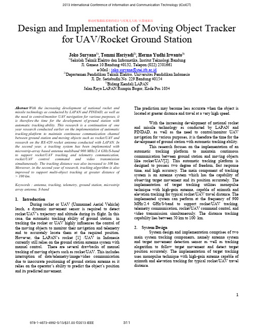
Design and Implementation of Moving Object Tracker for UAV/Rocket Ground StationJoko Suryana1), Tommi Hariyadi2), Herma Yudhi Irwanto3)1)Sekolah Teknik Elektro dan Informatika, Institut Teknologi BandungJl. Ganesa 10 Bandung 40132, Telepon (022) 2501661e-Mail : joko.suryana@stei.itb.ac.id2)Departemen Pendidikan Teknik Elektro, Universitas Pendidikan IndonesiaJl. Dr. Setiabudhi No. 229 Bandung 401543)Bidang Kendali LAPANJalan Raya LAPAN Rumpin Bogor, Kode Pos 1034Abstract With the increasing development of national rocket and missile technology as conducted by LAPAN and PINDAD, as well as the need to control/monitor UAV navigation for various purposes, itis therefore the time for the development of ground station with automatic tracking ability. This research is a continuation of one year research conducted earlier on the implementation of automatic tracking platform to maintain continuous communication channel between ground station and moving objects such as rocket/UAV and research on the RX-420 rocket antenna conducted with LAPAN. In the second year, a tracking system has been implemented with microstrip-array based antenna multiband 900 MHz/2.4 GHz/S-bandto support rocket/UAV tracking and telemetry communication, rocket/UAV control command and video transmission simultaneously. The tracking distance was also increased to 100 km. Moreover, in the second year of research, tracking algorithm is also improved to support multi-object tracking at greater distance of > 100 km.Keywords : antenna, tracking, telemetry, ground station, microstrip array antenna, S-band1.IntroductionDuring rocket or UAV (Unmanned Aerial Vehicle) lauch, a dynamic movement sensor is required to detect rocket/UAV’s trajectory and altitude during its flight. In this case, the automatic tracking ability of ground station in tracking the rocket or UAV highly influences the control of the moving objects to monitor their navigation and telemetry and to accurately locate them at the required position. However, the LAPAN’s rocket [1] /UAV in Indonesia currently still relies on the ground station antenna system with manual control. There are several drawbacks of manual tracking of moving objects such as rocket/UAV. This includes interruption of data/telemetry/image/video communication due to inaccurate positioning of ground station antenna as it relies on the operator’s ability to predict the object’s position and its predicted movement. The prediction may become less accurate when the object is located at greater distance and travel at a very high speed.With the increasing development of national rocket and missile technology as conducted by LAPAN and PINDAD, as well as the need to control/monitor UAV navigation for various purposes, it is therefore the time for the development of ground station with automatic tracking ability.This research focuses on the implementation of an automatic tracking platform to maintain continuous communication between ground station and moving objects like rocket/UAV[2]. This automatic tracking platform is designed to possess two degree of freedom, fast response time, and high accuracy. The main component of tracking system is an antenna system which has the capability of observing target movement and its position accurately. The implementation of target tracking utilizes monopulse technique with high-gain antenna, capable of azimuth and elevation tracking for typical rocket/UAV travel distance. The implemented system can perform at the frequency of 900 MHz/2.4 GHz/S-band to support rocket/UAV tracking, telemetry communication, rocket/UAV command control, and video transmission simultaneously. The distance tracking capability lies between 50 km to 100 km.2.System DesignSystem design and implementation comprises of two main system tracking components, namely antenna system and target movement detection sensor as well as tracking alogarithm to follow target movement and detect target position accurately. The implementation of target tracking uses monopulse technique with high-gain antenna capable of azimuth and elevation tracking for typical rocket/UAV travel distance.移动对象跟踪系统的设计与实现无人机/火箭地面站1During the implementation of m MHz/2.4 GHz/S-band tracking system wh rocket/UAV tracking, telemetry communication command control and video transmission, se steps were applied. First, tracking system w antenna 900 MHz/2.4 GHz/S-band was impleme Second, a tracking system with t simultaneously perform telemetry co rocket/UAV control command and video tran developed. Third, tracking distance of 50 km wa to 100 km. Fourth, tracking algorithm to suppo movement tracking was developed. Fifth, evaluation of tracking platform both indoor (limtest) and outdoor for field rocket/UAV t conducted.3. Results and DiscussionThe development of tracking system w900 MHz/2.4 GHz/S-band antenna has been con research to support rocket/UAV trackin communication, rocket/UAV control comman transmission simultaneously. The tracking dista has also been increased to 100 km with impr alogarithm to support muti-object tracking distance capability of > 100 km.The second year research study designsix main research activities, namely: selectio system, selection of tracking technique, selecti algorithm, measurement of module performan testing.3.1. High-Gain Antenna System Multiband 1DesignAt this stage, the activities involved arantenna type with multiband 1.7 – 2.5 GHz higher gain to achieve longer distance reach. Th by antenna design, realization, and testing u available at Radio and Microwave Telec Laboratory (LTRGM).Figure 1. The New Antenna Trackingmultiband 900hich supports n, rocket/UAV everal working with multiband ented.the ability toommunication, nsmission was as increased up ort multi-object performancemited manuver tracking were with multiband nducted in this ng, telemetry nd and video ance capability roved tracking with greater n comprises of on of antenna ion of tracking nce, and field 1.7 – 2.5 GHz re: selection of z ability, with his is followed using facilities communicationgThe selected antenna in the parabolic antenna as conducThe 5 subarray antennas cross dip microstrip was used, as seen in F is clearly shown in Figure 2.While the SWR simulpattern can be observed in FigureFigure 2. Subarray CFigure 3. VSWR SimFigure 4. Radiation Patter3.2. Implementation of HighMultiband 1.7 – 2.5 GHzIn order to improve Tdependency on materials, the im Antenna System Multiband ulilocal market, which is FR-4. Th 2this research no longer usescted in the previous research. pole 4 x 4 V and 4 x 4 H with Figure 1. Each of the subarray lation results and radiation 3 and Figure 4, respectively.Crossdipole VHmulation Resultrn Simulation Resultsh-Gain Antenna System TKDN and reduce import- mplementation of High-gain itizes materials available inhe antenna implementation isbased on the usage of crossdipole to suppor horizontal polarization operation. A photo of th antenna is shown in Figure 5 and 6.Figure 5. Implementation of Subarray Antenna Cro PhotoFigure 6. The Result of Antenna 4 x 4 V and 4 x 4 H3.3. Measurement of High-Gain AntenMultiband 1.7 – 2.5 GHzThe measurement of multiband anincludes: gain, radiation pattern, bandwidth, b VSWR. Figure 7 and 8 show the VSWR measu and radiation pattern measurement results.rt vertical and e implementedossdipole VHImplementationnna System ntenna system beamwidth and urement set upFigure 7. VSWR MeaFigure 8. Radiation Pat3.4. Improvement of Tracking PIn this activities, selecti rocket/UAV tracking was condu technique involved the use of fo represent the four quadrants: u quadrant. Each antenna is connec and it was then connected to a ppower detector was connected to command the actuator to furthethe antenna, controlling whether elevation movement or azimuth the diagram block of trackin implementation.Figure 9. A Diagram block of Dual MBandpass FilterFigure 10. Tracki3asurement Set-up.ttern MeasurementProcessor ion of tracking technique foructed. The selected tracking four receiver antennas which upper, lower, left and right ted to a BPF (bandpass filter)power detector. The output of a microprocessor which willer command motor driver for r the antenna should follow movement. The following is g system and its hardwareMotor Processor Driver SystemPower Detectoring Modules3.5.Realization of Azimuth and Elevation Driver withHigher PowerIn this activity, azimuth and elevation driver system with two electrical motors and gear system have been designed. In order to start the two motors, a power driver is required in which its control is done through PWM (Pulse Width Modulation) with microprosesor control.Figure 11. The antenna installed at Dual Motor PlatformThe selected motor specification can be used to support a load, weighed similar to parabolic antenna/reflector which will be used as monopulse system. In order to support and control the new antenna’s load, adjustment was made in the tracking platform. Therefore, the azimuth driver motor and the elevation driver motor were replaced with motors operating at higher power. Figure 11 shows the tracking platform with dual motor.3.6.Integration of Tracking Command Module withAntenna ModuleIntegration and re-adjustment of parameter settings were made for tracking techique implementation in the new antenna system and in new dual motor system. The selected tracking technique utilizes four receiver antennas which represent the four quadrants namely: upper, lower, left, and right quadrant. Each antenna was connected to a Low Noise Amplifier (LNA) and which was then connected to power detector.The output of power detector was connected to a microprocessor which will command the actuator to further command motor driver for the antenna, controlling whether the antenna should follow elevation movement or azimuth movement. Figure 12 shows the integration of RF sub-system with antenna and dual motor platform.Figure 12. A Photo of the Integration of Control Module andAntenna3.7.Tracking Function TestingFigure 13. A Photo of Performance Measurement of ObjectMovement DetectionIn order to conduct tracking function test, signal generator, transmitting antenna which represents UAV or rocket signals and 2 (two) voltmeter appliances for right and left channel observation or upper and lower channel observation are required.The monopulse system is based on object movement detection utilizing the changes in signal received between Right-Left and Upper-Lower. Right and left channel are used by the tracking system to detect any azimuth movement, while upper and lower channel are used to detect any elevation. A photo of tracking function is shown in Figure 13.4Target to the right Target to the leftFigure 14. Object Detection Result Photo4.ConclusionFrom the above research findings and discussion, it can be concluded that a multiband antenna tracking system has been implemented successfully using four quadrant microstrip-subarrays on 900 MHz/2.4 GHz/S-band. Laboratory test results suggest that the tracking system is able to detect any moving objects in term of its directional changes, which is indicated by changes in multimeter voltage value towards power detector readings. Thus, our prototyped is ready to be integrated in the ground station to support rocket / UAV tracking and telemetry communications. REFERENCES[1].Joko Suryana dan Herma Yudhi, ”Perancangan danImplementasi Antena Payload/Telemetri/GPS Corformal pada Sistem Roket LAPAN RX-420.” Seminar Nasional RADAR IV, LIPI, 2010 di Jogjakarta[2].Joko Suryana dkk, “Laporan Akhir SINAS 2012”, RisetInsentif Nasional 2012, Kemenristek5。

New FouNdCoNNeCtivityNFC instantly connects consumers with brand owners, retailers and service providers,bringing physical media to a completely new level of consumer excitement.Embedded NFC tags in posters, signs, menus, labels and business cards, immediately launch mobile phone applications or connect the user to social media websites. NFC means UPM RFID, the world leader in Near Field Communication.NFC tags from UPM RFIDUPM RFID is driven by innovation and a desire to be at the forefront of new technology. For many years NFC has been part of an RFID portfolio that provides solutions to the most demanding applications of our customers worldwide.NFC is a short-range standards based wireless communications technology operating in the 13.56 Mhz frequency band. Based on RFID technology, NFC uses inductivemagnetic field coupling to facilitate communication between phones and media content. NFC tags can carry significantly more data than bar codes, URLs or QR codes, are more secure and can be password protected, unlike their printed counterparts. For trend setters everywhere NFC technology is the next big thing.......• I nformation and services • N ew functionalities • Social networks • E ntertainment and mediaNFC, INtRoDUCINg a NEw aND INtUItIvEway to USE yoURSMaRtPhoNEFoR aCCESSINg:NFC - the smart solutionfor smart brandsthere are two stages to every consumer decision, point of purchase and point of use. NFC adds value to both of them.Packaging is often considered the ‘silent salesman’ on the shelf. thanks to NFC, packaging and labels can project a product’s presence far beyond the shelf. the ‘silent salesman’ now hasa voice, allowing brand owners and customersto communicate directly with each other, share experiences, take advantage of special promotions or just socialize and network with other brand users.via location dependent social networking sites like google’s hotPot, embedded NFC tags can provide more information about:• Individual products• Consumer endorsements• User manuals• Sustainability and recycling• Brand values NFC – for an enhancedretail experienceNFC gives brand owners and retailers an opportunityto work together, creating effective targeted salespromotions. NFC smart posters near entrances canmake tailored purchase suggestions to customers,while posters at the end of supermarket aisles canprovide real-time information on current special offers.NFC – it’s a wholenew gameNFC brings games developers the possibility toenter a completely new world of opportunity.games can be linked to the on-going saleof game specific merchandise with NFCembedded tags. these products will benecessary to complete tasks or proceed to thenext level. via dedicated social networkingmedia gamers can trade with each other foritems they require, such as clothing or cardsthey don’t have.“thE FUtURE IS NFC”, Cto, StEvE hoRowItz *“MEgaoPPoRtUNIty”googLE, CEo, ERIC SChMIDt *04/2011 e N G X 204。
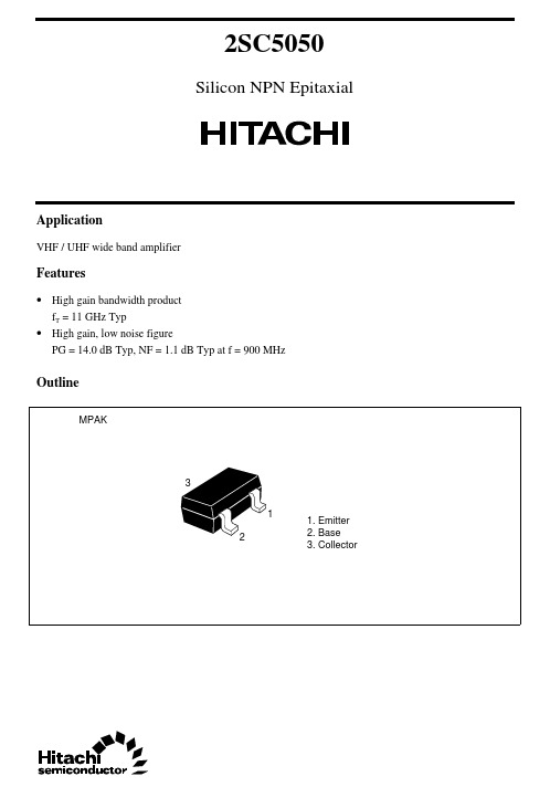
2SC5050Silicon NPN EpitaxialApplicationVHF / UHF wide band amplifierFeatures• High gain bandwidth product= 11 GHz TypfT• High gain, low noise figurePG = 14.0 dB Typ, NF = 1.1 dB Typ at f = 900 MHzOutline2SC50502Absolute Maximum Ratings (Ta = 25°C)ItemSymbol Ratings Unit Collector to base voltage V CBO 15V Collector to emitter voltage V CEO 8V Emitter to base voltage V EBO 1.5V Collector currentI C 50mA Collector power dissipation P C 150mW Junction temperature Tj 150°C Storage temperatureTstg–55 to +150°CElectrical Characteristics (Ta = 25°C)ItemSymbol Min Typ Max Unit Test conditions Collector to base breakdown voltageV (BR)CBO 15——V I C = 10 µA, I E = 0Collector cutoff current I CBO ——10µA V CB = 12 V, I E = 0I CEO ——1mA V CE = 8 V, R BE = ∞Emitter cutoff current I EBO ——10µAV EB = 1.5 V, I C = 0DC current transfer ratio h FE 50120250V CE = 5 V, I C = 20 mA Collector output capacitance Cob —0.6 1.1pF V CB = 5 V, I E = 0, f = 1 MHz Gain bandwidth product f T 8.011.0—GHz V CE = 5 V, I C = 20 mA S21 Parameter |S21|—13.5—dB V CE = 5 V, I C = 20 mA,f = 1000 MHz Power gain PG 11.014.0—dB V CE = 5 V, I C = 20 mA,f = 900 MHz Noise figureNF—1.12.0dB V CE = 5 V, I C = 5 mA,f = 900 MHzNote:Marking is “YZ–”.Attention: This device is very sensitive to electro static discharge.It is recommended to adopt appropriate cautions when handling this transistor.See characteristic curves of 2SC4926.2SC50503Hitachi CodeJEDECEIAJWeight (reference value)MPAK—Conforms0.011 gUnit: mm元器件交易网Cautions1.Hitachi neither warrants nor grants licenses of any rights of Hitachi’s or any third party’s patent,copyright, trademark, or other intellectual property rights for information contained in this document.Hitachi bears no responsibility for problems that may arise with third party’s rights, includingintellectual property rights, in connection with use of the information contained in this document.2.Products and product specifications may be subject to change without notice. Confirm that you have received the latest product standards or specifications before final design, purchase or use.3.Hitachi makes every attempt to ensure that its products are of high quality and reliability. However,contact Hitachi’s sales office before using the product in an application that demands especially high quality and reliability or where its failure or malfunction may directly threaten human life or cause risk of bodily injury, such as aerospace, aeronautics, nuclear power, combustion control, transportation,traffic, safety equipment or medical equipment for life support.4.Design your application so that the product is used within the ranges guaranteed by Hitachi particularly for maximum rating, operating supply voltage range, heat radiation characteristics, installationconditions and other characteristics. Hitachi bears no responsibility for failure or damage when used beyond the guaranteed ranges. Even within the guaranteed ranges, consider normally foreseeable failure rates or failure modes in semiconductor devices and employ systemic measures such as fail-safes, so that the equipment incorporating Hitachi product does not cause bodily injury, fire or other consequential damage due to operation of the Hitachi product.5.This product is not designed to be radiation resistant.6.No one is permitted to reproduce or duplicate, in any form, the whole or part of this document without written approval from Hitachi.7.Contact Hitachi’s sales office for any questions regarding this document or Hitachi semiconductor products.Hitachi, Ltd.Semiconductor & Integrated Circuits.Nippon Bldg., 2-6-2, Ohte-machi, Chiyoda-ku, Tokyo 100-0004, Japan Tel: Tokyo (03) 3270-2111 Fax: (03) 3270-5109Copyright ' Hitachi, Ltd., 1999. All rights reserved. Printed in Japan.Hitachi Asia Pte. Ltd.16 Collyer Quay #20-00Hitachi TowerSingapore 049318Tel: 535-2100Fax: 535-1533URLNorthAmerica : http:/Europe : /hel/ecg Asia (Singapore): .sg/grp3/sicd/index.htm Asia (Taiwan): /E/Product/SICD_Frame.htm Asia (HongKong): /eng/bo/grp3/index.htm Japan : http://www.hitachi.co.jp/Sicd/indx.htmHitachi Asia Ltd.Taipei Branch Office3F, Hung Kuo Building. No.167, Tun-Hwa North Road, Taipei (105)Tel: <886> (2) 2718-3666Fax: <886> (2) 2718-8180Hitachi Asia (Hong Kong) Ltd.Group III (Electronic Components)7/F., North Tower, World Finance Centre,Harbour City, Canton Road, Tsim Sha Tsui,Kowloon, Hong Kong Tel: <852> (2) 735 9218Fax: <852> (2) 730 0281 Telex: 40815 HITEC HXHitachi Europe Ltd.Electronic Components Group.Whitebrook ParkLower Cookham Road MaidenheadBerkshire SL6 8YA, United Kingdom Tel: <44> (1628) 585000Fax: <44> (1628) 778322Hitachi Europe GmbHElectronic components Group Dornacher Stra§e 3D-85622 Feldkirchen, Munich GermanyTel: <49> (89) 9 9180-0Fax: <49> (89) 9 29 30 00Hitachi Semiconductor (America) Inc.179 East Tasman Drive,San Jose,CA 95134 Tel: <1> (408) 433-1990Fax: <1>(408) 433-0223For further information write to:。
2021.10设计研发2-18GHz超宽带斜极化水平全向天线设计徐瑶俊,樊雪婷,郭庆功(四川大学电子信息学院,四川成都,610065)摘要:设计了一款2-lSGHz斜极化的全向天线,天线由一个超宽带水平全向的双锥天线和一个五层斜极化器构成。
通过增加卷边结构以及优化双锥天线母线长度,改善了超宽带双锥天线低频增益不足和高频方向图裂瓣的现象,釆用五层极化栅结构使辐射电场由垂直极化均匀的转换为45°斜极化。
使天线在2-18GHZ内电压驻波比(VSWR)小于2,不圆度小于3.5dB,0.89<|£fl|/<1.15,165°<AE e-5,<186°,具有良好的斜极化性能。
关键词:全向天线;超宽带;斜极化;双锥天线Slant-Polarized Horizontal Omnidirectional Antenna for2-18GHzUWB ApplicationsXu Yaojun,Fan Xueting,Guo Qinggong(School of electronic information,Sichuan University,Chengdu Sichuan,610065) Abstract:The article designed a2~18GHz obliquely polarized omnidirectional antenna.The antenna consists of an ultra wideband horizontal omnidirectional biconical antenna and a five layer t订ted polarizer.By increasing the curl strueture and optimizing the bus length of the biconical antenna, the phenomenon of low-frequency gain deficiency and high-frequency pattern split of the ultra wideband biconical antenna is improved.The radiation electrie field is uniformly converted from vertical polarization to45°oblique polarization by using a five layer polarization grid structure.The VSWR is less than2,roundness is less than 3.5db,0.89<|场|/隔<1.15,165。
PART NUMBER UPC2710TUPC2713TPACKAGE OUTLINET06T06 SYMBOLSPARAMETERS AND CONDITIONS UNITS MIN TYP MAX MIN TYP MAX I CC Circuit Current (no signal)mA 16222991215G S Small Signal GaindB 303336.5262933f U Upper Limit Operating Frequency(The gain at f U is 3 dB down from the gain at 0.1 GHz)GHz 0.71.00.91.2∆G S Gain Flatness, f = 0.1 ~ 0.6 GHz dB ±0.8f = 0.1∼ 0.8 GHz ±0.8P SAT Saturated Output PowerdBm 1113.547P 1dB Output Power at 1dB Compression Point dBm 7.5-4NF Noise Figure dB 3.553.24.5RL IN Input Return Loss dB 361013RL OUT Output Return Loss dB 91269ISOL IsolationdB 34393540∆G T Gain -Temperature CoefficientdB/°C -0.006-0.016R THThermal Resistance (Junction to Ambient)°C/W200200The UPC2710T and UPC2713T are Silicon Monolithic inte-grated circuits manufactured using the NESAT III process.These devices are suitable for applications which require high gain and wide-band operation. They are designed for low cost gain stages in cellular radios, GPS receivers, DBS tuners,PCN, and test/measurement equipment.NEC's stringent quality assurance and test procedures en-sure the highest reliability and performance.DESCRIPTIONFEATURES•FREQUENCY RESPONSE: 1.5 GHz • HIGH GAIN: 33 dB (UPC2710T)•SATURATED OUTPUT POWER: +13.5 (UPC2710T)•INTERNAL CURRENT REGULATION MINIMIZES GAIN CHANGE OVER TEMPERATURE • 5 V SINGLE SUPPLY VOLTAGE •SUPER SMALL PACKAGE•TAPE AND REEL PACKAGING OPTION AVAILABLEGAIN vs. FREQUENCYFrequency, f (GHz)G a i n , G S (d B )ELECTRICAL CHARACTERISTICS (T A = 25 °C, f = 0.5 GHz, V CC = 5 V)California Eastern Laboratories元器件交易网ABSOLUTE MAXIMUM RATINGS 1 (T A = 25°C)SYMBOLSPARAMETERS UNITS RATINGSV CC Supply Voltage V 6P IN Input Power dBm +10P T Power Dissipation mW 2802T OP Operating Temperature °C -40 to +85T STGStorage Temperature°C-55 to +150Notes:1. Operation in excess of any one of these parameters may result in permanent damage.2.Mounted on 50 x 50 x 1.6 mm epoxy glass PWB (T A = +85°C).RECOMMENDEDOPERATING CONDITIONSSYMBOL PARAMETER UNITS MIN TYP MAX V CCSupply VoltageV4.55.05.5UPC2710T, UPC2713TTEST CIRCUIT** UPC2710T onlyUPC2710TNOISE FIGURE ANDINSERTION GAIN vs. FREQUENCYUPC2713TNOISE FIGURE ANDINSERTION GAIN vs. FREQUENCYCIRCUIT CURRENT vs. VOLTAGETYPICAL PERFORMANCE CURVES (T A = 25°C)Supply Voltage, V CC (V)Operating Temperature, T OP (°C)C i r c u i t C u r r e n t , I C C (m A )C i r c u i t C u r r e n t , I C C (m A )I n s e r t i o n P o w e r G a i n , G P (d B )I n s e r t i o n P o w e r G a i n , G P (d B )CIRCUIT CURRENT vs. TEMPERATUREFrequency, f (GHz)Frequency, f (GHz)N o i s e F i g u r e , N F (d B )N o i s e F i g u r e , N F (d B )元器件交易网XX: Typical SSB Third Order Intercept PointUPC2710T, UPC2713TTYPICAL PERFORMANCE CURVES (T A = 25° C)UPC2713TRETURN LOSS vs. FREQUENCYUPC2710TPOWER vs. FREQUENCY UPC2713TPOWER vs. FREQUENCYP o w e r (d B m )P o w e r (d B m )I n p u t R e t u r n L o s s , R L I N (d B )O u t p u t R e t u r n L o s s , R L O U T (d B )I n p u t R e t u r n L o s s , R L I N (d B )O u t p u t R e t u r n L o s s , R L O U T (d B )Frequency, f (GHz)Frequency, f (GHz)Frequency, f (GHz)I s o l a t i o n , I S O L (d B )I s o l a t i o n , I S O L (d B )Frequency, f (GHz)Frequency, f (GHz)Frequency, f (GHz)0.1 0.3 1.0 3.0-10-20-30-40UPC2710TISOLATION vs. FREQUENCYUPC2713TISOLATION vs. FREQUENCYUPC2710TRETURN LOSS vs. FREQUENCYX: Typical SSB Third Order Intercept Point元器件交易网N o i s e F i g u r e , N F (d B )Frequency, f (GHz)UPC2710TOUTPUT POWER vs.INPUT POWER AND VOLTAGEUPC2713TOUTPUT POWER vs.INPUT POWER AND VOLTAGENOISE FIGURE vs. FREQUENCYO u t p u t P o w e r , P O U T (d B m )Input Power, P IN (dBm)O u t p u t P o w e r , P O U T (d B m )Input Power, P IN (dBm)UPC2713TOUTPUT POWER vs.INPUT POWER AND TEMPERATUREUPC2710TOUTPUT POWER vs.INPUT POWER AND TEMPERATUREO u t p u t P o w e r , P O U T (d B m )Input Power, P IN (dBm)O u t p u t P o w e r , P O U T (d B m )Input Power, P IN (dBm)TYPICAL PERFORMANCE CURVES (T A = 25° C)UPC2710T, UPC2713T元器件交易网TYPICAL SCATTERING PARAMETERS (T A = 25° C)V CC = 5 V, I CC = 12 mAUPC2713T0.10 0.322 -0.337.7 -5.9 0.013 17.1 0.200 -11.7 1.06 31.50.20 0.346 3.338.8 -17.0 0.01219.8 0.208 -15.4 1.07 31.80.30 0.383 2.1 40.2 -28.0 0.009 22.5 0.231 -23.5 1.21 32.10.40 0.429 -1.7 41.6 -40.4 0.009 25.1 0.258-34.2 1.10 32.40.500.465 -9.4 42.1 -54.1 0.012 27.8 0.273 -47.2 0.8632.50.60 0.486-17.842.3 -68.3 0.013 30.5 0.305 -60.9 0.7932.50.700.487 -27.241.1 -83.2 0.013 33.1 0.319 -77.80.82 32.30.80 0.468 -36.5 39.1 -97.9 0.013 35.80.320 -96.20.89 31.90.90 0.423 -44.535.4-111.7 0.013 38.5 0.297 -115.4 1.04 31.01.00 0.392 -50.3 32.9 -123.4 0.01441.20.260 -128.2 1.1030.41.100.349 -56.6 30.0 -135.5 0.014 43.9 0.240 -142.2 1.2229.61.20 0.301 -61.0 26.8-146.8 0.015 46.6 0.216 -156.3 1.31 28.61.30 0.257 -63.2 23.8 -156.8 0.016 49.2 0.192 -169.7 1.40 27.51.40 0.217-63.5 21.1 -165.9 0.016 51.6 0.173 176.0 1.5626.51.500.184-59.918.8-174.20.01754.50.155162.31.6525.50.10 0.350 -21.8 21.9 -8.1 0.006 25.6 0.286 -10.3 3.0726.80.20 0.290 -33.1 22.0 -25.3 0.00624.9 0.298-16.1 3.17 26.90.30 0.243 -41.7 22.1-37.3 0.007 23.7 0.313-25.6 2.7726.90.40 0.207 -47.322.3 -48.6 0.007 22.40.327-35.2 2.7827.00.50 0.185 -50.5 22.4 -60.00.007 21.6 0.336-45.4 2.78 27.00.60 0.176 -54.0 22.6-72.70.00820.1 0.348 -56.9 2.41 27.10.700.161-57.5 22.8-85.7 0.008 19.00.359 -69.0 2.3927.10.80 0.148 -60.2 22.9-100.7 0.009 18.3 0.366-82.9 2.13 27.20.90 0.127 -63.922.8-114.8 0.009 17.2 0.366-96.8 2.15 27.21.00 0.111-62.922.3-132.00.00916.4 0.359-111.8 2.23 27.01.10 0.097 -56.5 21.6 -147.6 0.010 15.7 0.343 -126.8 2.12 26.71.20 0.095 -48.2 20.6 -163.1 0.010 14.4 0.320 -142.3 2.2426.31.30 0.098-40.118.9-177.8 0.010 13.1 0.291-156.6 2.4725.51.40 0.110 -35.7 17.6 168.3 0.010 12.0 0.263-171.7 2.6824.91.50 0.129 -34.615.6 154.8 0.011 11.8 0.234 174.3 2.77 23.91.60 0.145 -36.2 14.2 142.7 0.01211.2 0.208 160.8 2.81 23.01.70 0.161-40.0 12.6 130.5 0.013 10.8 0.185 147.1 2.92 22.01.80 0.179 -44.7 11.4 120.9 0.014 9.8 0.164132.6 3.02 21.11.90 0.191 -50.3 10.2 110.1 0.015 7.5 0.148 119.5 3.1520.12.000.197-56.19.3100.80.0165.50.137107.43.2319.4FREQUENCYS 11S 21S 12S 22 K 1S 21(GHz)MAG ANG MAG ANG MAG ANG MAG ANG(dB)V CC = 5 V, I CC = 22 mAUPC2710TUPC2710T, UPC2713TNote:1. K factor calculations:K = 1 + | ∆ | - |S 11| - |S 22|2222 |S 12 S 21|, ∆ = S 11 S 22 - S 21 S 12FREQUENCYS 11S 21S 12S 22 K 1S 21(GHz)MAG ANG MAG ANG MAG ANG MAG ANG (dB)EQUIVALENT CIRCUITUPC2710T, UPC2713TPACKAGE OUTLINE (Units in mm)UPC2710T/UPC2713T PACKAGE OUTLINE T06-0.05 +0.10±0.1LEAD CONNECTIONSPART NUMBER QTY UPC2710T-E33K/Reel UPC2713T-E33K/ReelEmbossed Tape, 8 mm wide.ORDERING INFORMATIONRECOMMENDED P.C.B. LAYOUT (Units in mm)Note:All dimensions are typical unless otherwise noted.1.INPUT2.GND3.GND4.OUTPUT5.GND6.V CC(Top View)(Bottom View)C 1FUPC2710TUPC2713TNote: Package Markings:C1F - UPC2710TC1J - UPC2713T532161.0 0.5 MIN0.951.0 EXCLUSIVE AGENT FOR NEC Corporation RF & MICROWAVE SEMICONDUCTOR PRODUCTS - U.S. & CANADACALIFORNIA EASTERN LABORATORIES, INC· Headquarters · 4590 Patrick Henry Drive · Santa Clara, CA 95054-1817 · (408) 988-3500 · Telex 34-6393/FAX (408) 988-0279DATA SUBJECT TO CHANGE WITHOUT NOTICE。
An Improved High Gain and Wide Bandwidth Operational Amplifier for the SHA Circuit in a Pipelined ADCYu Wang1, 2, Hai-gang Yang1,*, Member, IEEE, Zhen-hua Ye1,2, Hui Zhang1,2, and Fei Liu11Institute of Electronic, Chinese Academy of Science(CAS),Beijing 100190, China2Graduate University of CAS, Beijing 100049,China* Email: yanghg@AbstractThis paper presents a high gain and wide bandwidth fully differential operational amplifier (op amp) used in a sample and hold amplifier (SHA) circuit for a 12bit, 50Ms/s pipelined ADC. The gain-boosted technique is adopted to achieve a high gain without reduction of the output swing, while a new frequency compensation method is developed to compensate the bandwidth degradation caused by the gain-boosted structure. Simulation results show that the amplifier exhibits a gainof 114dB, unity gain bandwidth of 721MHz, and 2V output range from a single 3.3V supply. A sample and hold circuit employing the amplifier is implemented in a commercial 0.35P m CMOS process, the measurement results show that the amplifier should meet the requirement for the pipelined ADC operating at up to 50MHz sampling clock.1.In troductionModern communication system drives the continued development of ADCs with high resolution and high sampling rate. A front-end sample and hold amplifier is mandatory to avoid degradation of the ADC’s effective resolution at a high input frequency.[1]~[3] The operational amplifier should present high gain, high linearity, wide bandwidth and good frequency response property in order not to impact the converter’s performance.To achieve a high gain, the telescope architecture and gain-boosted technique is considered [1][2]. However, the gain-boosting amplifier limits the frequency bandwidth and phase margin. To solve such problems, a frequency compensation method by adding compensation capacitor at the output node of the auxiliary amplifier is proposed in this paper. It can restrain the Miller effect referring to the auxiliary amplifier, efficiently improve the unity gain bandwidth and phase margin of the main amplifier, and make the integrated amplifier work as a single-pole system in the range of unite-gain bandwidth, which improves the stability of the settling behavior. A high gain (over 114dB) op amp with wide unity gain bandwidth of 721MHz in a condition of 1pF load and 3.3V voltage supply is presented in this paper.A sample and hold circuit using this op amp based ona flip-around structure is fabricated in a commercial0.35P m CMOS process. The simulation results show that it achieves over 88dB SNDR and 89dB SFDR at 50MHz sample clock and consumes 27mW at 3.3V voltage supply. The measurement results verify the improvement of the proposed compensation method.2.Architecture and DesignThe op amp based on the gain-boosted telescope cascode architecture is the best choice for the high speed high resolution sample and hold circuit. Compared with it, the 2-stage structure and folded cascade both has their disadvantages. The former requires Miller compensation for stability, and also consumes more than twice power dissipates of a single stage. The later exhibits a lower achievable bandwidth though it has a larger range of input voltage [2]. The amplifier shown in Fig 1 adopts the gain-boosted technique to achieve the high gain and no output swing reduction. A new method of adding compensate capacitor at the output of auxiliary amplifier is proposed to improve the frequency performance. More theoretic analysis of the gain-boosted amplifier ispresented in section2.1.Fig 1 Improved gain-boosted telescope amplifier978-1-4244-5798-4/10/$26.00 ©2010 IEEE2.1Analysis and improvementA gain-boosted telescope circuit model is shown in Fig 2 (a). A small signal analysis of the proposed fully differential amplifier is based on such single-end model. As the auxiliary amplifier gives a negative feed-back at the gate voltage of M2, the output resistance is calculated as the equation (1) [1]:(1)2,1,2,0o o m out r r g A R |Where A 0 is the open loop gain of the gain boosting amplifier. g m,2 is the transconductance of M1. r o,1, r o,2is the output equivalent resistances of M1 and M2. Then, the output voltage gain is2,2,1,1,01,m o o m out m v g r r g A R g A |(2)Fig 2 (a) Gain boosting in cascade structure (b) Miller effect of C gs,2 in this circuit The frequency of the main pole is at the output node, which dominates the 3dB bandwidth of such gain-boosted op amp. The frequency of 3dB bandwidth is2,1,2,0311o o m load out Load db r r g A C R CZ (3) The frequency of the second pole, (at node X) isXm X C g 2, Z (4)As shown in Fig 2 (b), the parasitic capacitance at node X is 2C gd,1, C db,1 and C gsX . C gsX is the Miller effect of C gs,2 at node X, which is calculated as follows in such gain-boosted structure:)1(1112,,YX gs YXgs X gs gsX A C sA Z sZ C(5)Where Z gs is the impedance from the gate to the source of M2. A YX is the gain of node Y to node X. Consideringthe auxiliary amplifier as a ideal model, A YX is equal to (-A 0), and C gsX is)1()1(02,2,A C A C C gs YX gs gsX (6)Obviously, the parasitic capacitance at node X increases almost A 0 times because of the gain-boosting amplifier. It is concluded that the frequency of the pole at node X is pushed much closer to origin; so, the unity gain bandwidth is limited by the auxiliary amplifier. To restrain the Miller effect of C gsX , this paper presents a new method of adding the compensate capacitance at the output of the auxiliary amplifier (node Y) shown in Fig 1. This is because at high frequencies (as we approach the pole at node X), the compensate capacitor C c parallel connects with C gsY , dropping the gain of the auxiliary amplifier and suppressing the Miller effect of C gs,2. Then, in the unity gain bandwidth range, only one pole is dominated, which makes the amplifier stable like a single-pole system. So a gain-boosted differential op amp used this compensation technique is designed to meet the requirement of the high gain and wide bandwidth.2.2Simulation resultsThe amplifier simulation is carried out using the Spectre circuit simulator. Fig 3 compares the frequency response of the improved amplifier with the conventional one. It clearly represents that the phase margin is much improved due to the proposed compensation technique, and the subordinate pole of the integrated amplifier is pushed out of the unity gain bandwidth. The amplifierhas almost the same characters of a single pole system.Fig 3 Frequency performance comparison Table 1 lists a brief comparison between the improved amplifier (Ex1), the structure which is not compensated (Ex2) and Ref [4]. It shows that the improved amplifier could achieve much higher gain and wider bandwidth than the conventional op amp.Table 1. Performance comparisonsItem Ex.1Ex.2[4]A v (dB) 114 114 63.95GBW(MHz) 721 635 283PM(嘙)635461.9 Power(mW) 272719.94V oltage supply(V) 3.3 3.3 3.3 2.3The SHA circuit implementationA sample and hold amplifier was developed in 0.35P m CMOS process. Used for a 12bit,50Ms/s pipelined ADC, this sample and hold front-end is based on a flip-around structure, and achieves over 88dB SNDR and 89dB SFDR in the Spectre simulation condition. Fig 4 shows the schematic diagram; and the simulated spectrum is depicted in Fig 5. The results indicate that the improved amplifier supply a much more precise loop gain and anenough fast settling process in a closed loop circuit.Fig 4 Flip-flop Sample and hold structureFig 5 FFT Spectrum at 50M sample clock, 5M inputfrequency. 3.Measurement resultsA test chip of the sample and hold amplifier is fabricated in Charter 0.35P m 2P4M CMOS process. Fig 6 is the photo of the chip. The test wave of output is depicted as Fig 7. The wave shows the input sine wave was sampled at the end of the half clock period and hold for half a clock period. The output of the SHA satisfies the pipelined ADC requirement. Even though, the glitches are engendered by the disturbance of the non-ideal clockand wave scope. The further test will be carried on.Fig 6 Die photo of sample and hold circuitFig 7 SHA output wave at(a)10MHz sample clock (b)50MHz sample clock4.ConclusionA 114dB, 721MHz differential operational amplifier is designed, which adopts the gain-boosted technique. A compensate method is proposed to restrain the degradation of both bandwidth and phase margin derived from the gain-boosted technique. A SHA using this amplifier is developed, and tested under 50MHz sample clock. It consumes 28mW at 3.3V voltage supply, and is finally implemented in a 12bit pipelined ADC.Referen ces[1] Klaas Bult and Govert J.G.M.Green, A Fast-Settling CMOS Op Amp for SC Circuits with 90-dB DC gain, IEEE J ournal of Solid-State Circuits, vol25, No.6(1990)[2] Kush Gulti and Hae-Seung Lee, A High-Swing CMOS telescopic Operational Amplifier, IEEE Journal of Solid-State Circuits, vol 33, No.12(1998) [3] Ahmadi M M, A new modeling and optimization of gain-boosted cascode amplifier for high-speed and low-voltage applications , IEEE Trans Circuits System Ċ,53 (3) :169 (2006)[4] Ning Ning, Yu Qi and Wang Xiangzhan, A Novel Clock Feed-through Frequency Compensation for Fast-Setting of Folded-Cascode OTA, Chinese Journal of Semiconductors, V ol. 27, No.10 (2006).。