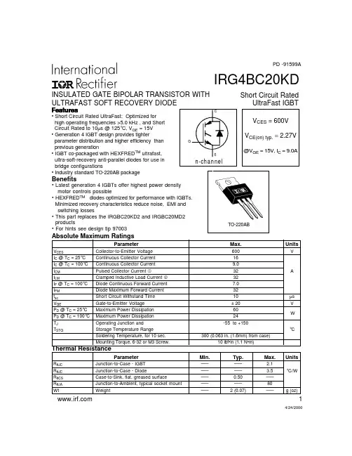
ParameterMax.UnitsV CESCollector-to-Emitter Voltage 600VI C @ T C = 25°C Continuous Collector Current 16I C @ T C = 100°C Continuous Collector Current 9.0I CM Pulsed Collector Current Q32AILMClamped Inductive Load Current R 32I F @ T C = 100°C Diode Continuous Forward Current 7.0I FM Diode Maximum Forward Current 32t sc Short Circuit Withstand Time 10µs V GEGate-to-Emitter Voltage± 20V P D @ T C = 25°C Maximum Power Dissipation 60P D @ T C = 100°C Maximum Power Dissipation 24T J Operating Junction and-55 to +150T STGStorage Temperature Range°CSoldering Temperature, for 10 sec.300 (0.063 in. (1.6mm) from case)Mounting Torque, 6-32 or M3 Screw.10 lbf•in (1.1 N•m)IRG4BC20KDINSULATED GATE BIPOLAR TRANSISTOR WITH ULTRAFAST SOFT RECOVERY DIODEFeaturesV CES = 600VV CE(on) typ. = 2.27V@V GE = 15V, I C = 9.0AShort Circuit RatedUltraFast IGBT4/24/2000• Short Circuit Rated UltraFast: Optimized for high operating frequencies >5.0 kHz , and Short Circuit Rated to 10µs @ 125°C, V GE = 15V • Generation 4 IGBT design provides tighterparameter distribution and higher efficiency than previous generation• IGBT co-packaged with HEXFRED TM ultrafast, ultra-soft-recovery anti-parallel diodes for use in bridge configurations• Industry standard TO-220AB packageBenefitsPD -91599AParameter Min.Typ.Max.UnitsR θJC Junction-to-Case - IGBT –––––– 2.1R θJC Junction-to-Case - Diode–––––– 3.5°C/WR θCS Case-to-Sink, flat, greased surface–––0.50–––R θJA Junction-to-Ambient, typical socket mount ––––––80WtWeight–––2 (0.07)–––g (oz)Thermal ResistanceAbsolute Maximum RatingsW• Latest generation 4 IGBTs offer highest power density motor controls possible• HEXFRED TM diodes optimized for performance with IGBTs. Minimized recovery characteristics reduce noise, EMI and switching losses• This part replaces the IRGBC20KD2 and IRGBC20MD2 products• For hints see design tip 97003 1IRG4BC20KDParameter Min.Typ.Max.Units Conditions Q g Total Gate Charge (turn-on)—3451I C = 9.0A Q ge Gate - Emitter Charge (turn-on)— 4.97.4nC V CC = 400V See Fig.8Q gc Gate - Collector Charge (turn-on)—1421V GE = 15V t d(on)Turn-On Delay Time —54—t r Rise Time —34—T J = 25°Ct d(off)Turn-Off Delay Time —180270I C = 9.0A, V CC = 480V t f Fall Time —72110V GE = 15V, R G = 50ΩE on Turn-On Switching Loss —0.34—Energy losses include "tail"E off Turn-Off Switching Loss —0.30—mJ and diode reverse recovery E ts Total Switching Loss —0.640.96See Fig. 9,10,14t sc Short Circuit Withstand Time 10——µs V CC = 360V, T J = 125°CV GE = 15V, R G = 50Ω , V CPK < 500Vt d(on)Turn-On Delay Time —51—T J = 150°C,See Fig. 11,14t rRise Time—37—I C = 9.0A, V CC = 480Vt d(off)Turn-Off Delay Time —220—V GE = 15V, R G = 50Ωt f Fall Time—160—Energy losses include "tail"E ts Total Switching Loss—0.85—mJ and diode reverse recovery L E Internal Emitter Inductance —7.5—nH Measured 5mm from package C ies Input Capacitance —450—V GE = 0V C oes Output Capacitance—61—pF V CC = 30V See Fig. 7C res Reverse Transfer Capacitance —14—ƒ = 1.0MHz t rr Diode Reverse Recovery Time —3755ns T J = 25°C See Fig.—5590T J = 125°C 14 I F = 8.0A I rr Diode Peak Reverse Recovery Current — 3.5 5.0A T J = 25°C See Fig.— 4.58.0T J = 125°C 15 V R = 200V Q rr Diode Reverse Recovery Charge —65138nC T J = 25°C See Fig.—124360T J = 125°C 16 di/dt = 200Aµs di (rec)M /dtDiode Peak Rate of Fall of Recovery —240—A/µs T J = 25°C See Fig.During t b—210—T J = 125°C 17Parameter Min.Typ.Max.Units ConditionsV (BR)CES Collector-to-Emitter Breakdown Voltage S 600——V V GE = 0V, I C = 250µA ∆V (BR)CES /∆T J Temperature Coeff. of Breakdown Voltage —0.49—V/°C V GE = 0V, I C = 1.0mA V CE(on)Collector-to-Emitter Saturation Voltage — 2.27 2.8I C = 9.0A V GE = 15V— 3.01—V I C = 16ASee Fig. 2, 5— 2.43—I C = 9.0A, T J = 150°C V GE(th)Gate Threshold Voltage 3.0— 6.0V CE = V GE , I C = 250µA ∆V GE(th)/∆T J Temperature Coeff. of Threshold Voltage —-10—mV/°CV CE = V GE , I C = 250µA g feForward Transconductance T 2.9 4.3—S V CE = 100V, I C = 9.0A I CES Zero Gate Voltage Collector Current ——250µAV GE = 0V, V CE = 600V——1000V GE = 0V, V CE = 600V, T J = 150°C V FM Diode Forward Voltage Drop — 1.4 1.7VI C = 8.0A See Fig. 13— 1.3 1.6I C = 8.0A, T J = 150°C I GES Gate-to-Emitter Leakage Current ——±100nAV GE = ±20VSwitching Characteristics @ T J = 25°C (unless otherwise specified)Electrical Characteristics @ T J = 25°C (unless otherwise specified)nsnsIRG4BC20KD 3Fig. 1 - Typical Load Current vs. Frequency(Load Current = I RMS of fundamental)Fig. 2 - Typical Output Characteristics Fig. 3 - Typical Transfer CharacteristicsIRG4BC20KDFig. 6 - Maximum Effective Transient Thermal Impedance, Junction-to-CaseFig. 5 - Typical Collector-to-Emitter Voltagevs. Junction TemperatureFig. 4 - Maximum Collector Current vs. CaseTemperatureIRG4BC20KD 5Fig. 7 - Typical Capacitance vs.Collector-to-Emitter VoltageFig. 8 - Typical Gate Charge vs.Gate-to-Emitter VoltageFig. 9 - Typical Switching Losses vs. GateResistance Fig. 10 - Typical Switching Losses vs.Junction TemperatureCollector-to-Emitter CurrentFig. 13 - Maximum Forward Voltage Drop vs. Instantaneous Forward Current0.11101000.40.81.21.62.02.42.83.2FM F I n s t a n t a n e o u s F o r w a r d C u r r e n t - I (A )Forward Voltage Drop - V (V)IRG4BC20KD 7Fig. 14 - Typical Reverse Recovery vs. di f /dtFig. 15 - Typical Recovery Current vs. di f /dtFig. 16 - Typical Stored Charge vs. di f /dt Fig. 17 - Typical di (rec)M /dt vs. di f /dt1002003004005001001000fdi /dt - (A/µs)R R Q - (n C )1001000100001001000fdi /dt - (A/µs)d i (r e c )M /d t - (A /µs )204060801001001000fdi /dt - (A/µs)t - (n s)r r 1101001001000fdi /dt - (A/µs)I - (A )I RR MIRG4BC20KDFig. 18a - Test Circuit for Measurement ofI LM , E on , E off(diode), t rr , Q rr , I rr , t d(on), t r , t d(off), t ft1t2Fig. 18b - Test Waveforms for Circuit of Fig. 18a, DefiningE off , t d(off), t fFig. 18c - Test Waveforms for Circuit of Fig. 18a,Defining E on , t d(on), t rFig. 18d - Test Waveforms for Circuit of Fig. 18a,Defining E rec , t rr , Q rr , I rrIRG4BC20KD 9V g G A T E S IG NA LDE V ICE U NDE R T E S TCUR RE N T D.U.T.V O LT A G E IN D.U.T.CUR RE N T IN D1t0t1t2Figure 19. Clamped Inductive Load TestCircuit Figure20. Pulsed Collector CurrentTest Circuit=480V4 X I C @25°CFigure 18e. Macro Waveforms for Figure 18a's Test CircuitIRG4BC20KDNotes:Q Repetitive rating: V GE =20V; pulse width limited by maximum junction temperature (figure 20)R V CC =80%(V CES ), V GE =20V, L=10µH, R G = 50Ω (figure 19)S Pulse width ≤ 80µs; duty factor ≤ 0.1%.T Pulse width 5.0µs, single shot.Case Outline TO-220AB0.55 (.022)0.46 (.018)3 X2.92 (.115)2.64 (.104)1.32 (.052)1.22 (.048)- B -4.69 (.185)4.20 (.165)3.78 (.149)3.54 (.139)- A -6.47 (.255)6.10 (.240)1.15 (.045) M IN4.06 (.160)3.55 (.140)3 X3.96 (.160)3.55 (.140)3 X 0.93 (.037)0.69 (.027)0.36 (.014) M B A M10.54 (.415)10.29 (.405)2.87 (.113)2.62 (.103)15.24 (.600)14.84 (.584)14.09 (.555)13.47 (.530)1.40 (.055)1.15 (.045)3 X2.54 (.100)2X1 2 34CONFORMS TO JEDEC OUTLINE TO-220ABD im e ns io ns in M illim e ters a nd (In c he s)LE A D A S S IG N M E N T S 1 - G A TE2 - C O LLE C TO R3 - EM IT TE R4 - C O LLE C TO RN O TE S :1 D IM E N S IO N S & T O LE R A N C IN G P E R A N S I Y 14.5M , 1982.2 C O N TR O LLIN G D IM E N S IO N : IN C H.3 D IM E N S IO N S A R E S H O W N M ILLIM E TE R S (IN C HES ).4 C O N FO R M S TO JE D E C O U TLIN E T O -220AB.IR WORLD HEADQUARTERS: 233 Kansas St., El Segundo, California 90245, USA Tel: (310) 252-7105IR EUROPEAN REGIONAL CENTRE: 439/445 Godstone Rd, Whyteleafe, Surrey CR3 OBL, UK Tel: ++ 44 (0)20 8645 8000IR CANADA: 15 Lincoln Court, Brampton, Ontario L6T3Z2, Tel: (905) 453 2200IR GERMANY: Saalburgstrasse 157, 61350 Bad Homburg Tel: ++ 49 (0) 6172 96590IR ITALY: Via Liguria 49, 10071 Borgaro, Torino Tel: ++ 39 011 451 0111IR JAPAN: K&H Bldg., 2F, 30-4 Nishi-Ikebukuro 3-Chome, Toshima-Ku, Tokyo 171 Tel: 81 (0)3 3983 0086IR SOUTHEAST ASIA: 1 Kim Seng Promenade, Great World City West Tower, 13-11, Singapore 237994 Tel: ++ 65 (0)838 4630IR TAIWAN:16 Fl. Suite D. 207, Sec. 2, Tun Haw South Road, Taipei, 10673 Tel: 886-(0)2 2377 9936Data and specifications subject to change without notice. 10/00元器件交易网Note: For the most current drawings please refer to the IR website at:/package/。