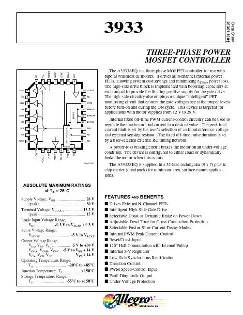
Data Sheet 26301.100†The A3933SEQ is a three-phase MOSFET controller for use with bipolar brushless dc motors. It drives all n-channel external power FETs, allowing system cost savings and minimizing r (DS)on power loss.The high-side drive block is implemented with bootstrap capacitors at each output to provide the floating positive supply for the gate drive.The high-side circuitry also employs a unique “intelligent” FETmonitoring circuit that ensures the gate voltages are at the proper levels before turn-on and during the ON cycle. This device is targeted for applications with motor supplies from 12 V to 28 V.Internal fixed off-time PWM current-control circuitry can be used to regulate the maximum load current to a desired value. The peak load-current limit is set by the user’s selection of an input reference voltage and external sensing resistor. The fixed off-time pulse duration is set by a user-selected external RC timing network.A power-loss braking circuit brakes the motor on an under-voltage condition. The device is configured to either coast or dynamically brake the motor when this occurs.The A3933SEQ is supplied in a 32-lead rectangular (9 x 7) plasticchip carrier (quad pack) for minimum-area, surface-mount applica-tions.3933FEATURES AND BENEFITSI Drives External N-Channel FETs I Intelligent High-Side Gate DriveI Selectable Coast or Dynamic Brake on Power Down I Adjustable Dead Time for Cross-Conduction Protection I Selectable Fast or Slow Current-Decay Modes I Internal PWM Peak Current Control I Reset/Coast InputI 120° Hall Commutation with Internal Pullup I Internal 5-V RegulatorI Low-Side Synchronous Rectification I Direction ControlI PWM Speed-Control Input I Fault-Diagnostic Output IUnder-Voltage ProtectionTHREE-PHASE POWER MOSFET CONTROLLER115 Northeast Cutoff, Box 15036Worcester, Massachusetts 01615-0036 (508) 853-********THREE-PHASE POWER MOSFET CONTROLLERCopyright © 1999, Allegro MicroSystems, Inc.Functional Block DiagramRECOMMENDED OPERATING CONDITIONSSupply Voltage, V BB ...................................... 15 V to 28 Vor, if V BB = V CCOUT ................................... 12 V ±10%Logic Input Voltage Range, V IN .............. -0.3 V to +4.8 V Sense Voltage Range, V SENSE ........................ -1 V to +1 V RC Resistance.......................................... 10 k Ω to 100 k ΩPWM Frequency, f PWM ....................... 20 kHz to 100 kHzLOW-SIDE Dwg. FP-045V 1 OF 3 HIGH-SIDE DRIVERSTO 1 OF 3MOTOR PHASES TO LCAP3933THREE-PHASE POWER MOSFET CONTROLLERELECTRICAL SPECIFICATIONS at T A = 25°C, V BB = V CCOUT = 12 V, C load = 1000 pF, C boot = 0.047 µF (unless noted otherwise).LimitsParameterSymbolConditionsMinTypMaxUnitsSupply CurrentQuiescent Current I BB RESET low, f PWM = 40 kHz –1619mA RESET high–1517mA Reference Voltage V LCAP4.755.0 5.25V Ref. Volt. Load Regulation ∆V LCAP(∆ILCAP)I LCAP = 0 to -2 mA –1025mV Output VoltageV CCOUTV BB = 28 V10.81213.2V Output Voltage Regulation∆V CCOUT(∆ICCOUT)V BB = 28 V, I CCOUT = 0 to -10 mA––25mV Digital Logic LevelsLogic Input Voltage V IH 2.0––V V IL ––0.8V Logic Input CurrentI IH V IH = 2 V –<1.010µA I ILV IL = 0.8 V-70–-130µA Gate DriveLow-Side Output Voltage V GLxH 9.510.511.5V V GLxL I GLx = 1 mA––0.30V High-Side Output Voltage V GHxH 9.010.511.5V V GHxL I GHx = 1 mA ––0.25V Low-Side Output t rGLx 1 V to 8 V –50–ns Switching Time t fGLx 8 V to 1 V –40–ns High-Side Output t rGHx 1 V to 8 V –100–ns Switching Time t fGHx 8 V to 1 V –100–ns DEAD Timet DEADI DEAD = 10 µA –3000–ns (Source OFF to Sink ON)I DEAD = 215 µA –180–nsContinued —NOTES: 1.Typical Data is for design information only.2.Negative current is defined as coming out of (sourcing) the specified device terminal.115 Northeast Cutoff, Box 15036Worcester, Massachusetts 01615-0036 (508) 853-50003933THREE-PHASE POWER MOSFET CONTROLLERELECTRICAL SPECIFICATIONS at T A = 25°C, V BB = V CCOUT = 12 V, C load = 0.001 µF, C boot = 0.047 µF (unless noted otherwise), continued.LimitsParameterSymbolConditions MinTypMaxUnitsBootstrap CapacitorBootstrap Charge Current I Cx 50100150mA Bootstrap Output Voltage V Cx Reference Sx9.510.511.5V Leakage CurrentI Cx High side switched high, Sx = V BB–1520µA Current LimitOffset Voltage V io –0±5.0mV Input bias current I SENSE ––-1.0µA RC Charge Current I RC 8509451040µA RC Voltage Threshold V RCL 1.0 1.1 1.2V V RCH 2.73.0 3.2V PWM frequency Rangef PWM Operating 20–100kHz Protection CircuitryUndervoltage Threshold UVLO Increasing V BB 9.710.210.7V Decreasing V BB 9.35–10.35V Boot-Strap Capacitor Volt.V CxSx V BB = 12 V 9.5––V High-Side Gate-Source Volt.V GHxSx – 6.3–V Fault Output VoltageV FAULT I O = 1 mA––0.8V Brake FunctionBrake Cap. Supply Current I BRKCAP V BB = 8 V, BRKSEL ≥ 2 V –30–µA Low-Side Gate VoltageV GLxHV BB = 0, BRKCAP = 8 V–6.6–VNOTES: 1.Typical Data is for design information only.2.Negative current is defined as coming out of (sourcing) the specified device terminal.3933THREE-PHASE POWER MOSFET CONTROLLERTerminalName1PGND 2RESET 3GLC 4SC 5GHC 6CC 7GLB 8SB 9GHB 10CB 11GLA 12SA 13GHA 14CA 15V CCOUT 16LCAP 17FAULT 18MODE 19V BB 20H121H322H223DIR 24BRAKE 25BRKCAP 26BRKSEL 27PWM 28RC 29SENSE 30REF 31DEAD 32AGNDRESET — A logic input used to enable the device, internally pulled up to V LCAP (+5 V). A logic HIGH will disable the device and force all gate drivers to 0 V, coasting the motor. A logic LOW allows the gate drive to follow commutation logic.This input overrides BRAKE.GLA/GLB/GLC — Low-side, gate-drive outputs for external NMOS drivers. External series-gate resistors (as close aspossible to the NMOS gate) can be used to control the slew rate seen at the power-driver gate, thereby controlling the di/dt and dv/dt of the SA/SB/SC outputs. Each output is designed and specified to drive a 1000 pF load with a rise time of 50 ns.SA/SB/SC — Directly connected to the motor, these terminals sense the voltages switched across the load. These terminals are also connected to the negative side of the bootstrap capaci-tors and are the negative supply connections for the floating high-side drive.GHA/GHB/GHC — High-side, gate-drive outputs for external NMOS drivers. External series-gate resistors (as close aspossible to the NMOS gate) can be used to control the slew rate seen at the power-driver gate, thereby controlling the di/dt and dv/dt of the SA/SB/SC outputs. Each output is designed and specified to drive a 1000 pF load with a rise time of 100 ns.CA/CB/CC — High-side connections for the bootstrap capaci-tors, positive supply for high-side gate drive. The bootstrap capacitor is charged to approximately V CCOUT when theassociated output SA/SB/SC terminal is low. When the output swings high, the voltage on this terminal rises with the output to provide the boosted gate voltage needed for n-channel power FETs.Terminal Descriptionscontinued next page115 Northeast Cutoff, Box 15036Worcester, Massachusetts 01615-0036 (508) 853-50003933THREE-PHASE POWER MOSFET CONTROLLERFAULT — Open-drain output to indicate fault condition; will go active high for any of the following:1 – invalid HALL input code,2 – high-side, gate-source voltage less than 7 V,3 – bootstrap capacitor not sufficiently charged, or4 – under-voltage condition detected at V CCOUT .The fault state for gate-source and bootstrap monitors are cleared at each commutation. If the motor has stalled, then the fault can only be cleared by toggling the RESET terminal or power-up sequence.MODE — A logic input to set current-decay method, internally pulled up to V LCAP (+5 V). When in slow-decay mode (logic HIGH), only the high-side FET is switched open during a PWM OFF cycle. The fast-decay mode (logic LOW) switches both the source and sink FETs.H1/H2/H3 — Hall-sensor inputs; internally pulled up to V LCAP (+5 V). Configured for 120° electrical spacing.DIR — A logic input to reverse rotation, see commutation logic table. Internally pulled up to V LCAP (+5 V).BRAKE — A logic input to short out the motor windings for a braking function. A logic HIGH will turn ON the low-side FETs, turn OFF the high-side FETs. Internally pulled up to V LCAP (+5 V). The braking torque applied will depend on the speed.BRKCAP — Connection for reservoir capacitor. This terminal is used to provide a positive power supply for the sink-drive outputs for a power-down condition. This will allow predict-able braking, if desired. A blocking diode to V CCOUT is re-quired. A 4.7 µF capacitor will provide 6.5 V gate drive for 300 ms. If a power-down braking option is not needed(BRKSEL = LOW) then this terminal should be tied to V CCOUT .BRKSEL — A logic input to enable/disable braking on power-down condition. Internally pulled up to V LCAP (+5 V). If held low, the motor will coast on a power-down condition.PWM — Speed control input, internally pulled up to V LCAP(+5 V). A logic LOW turns OFF all drivers, a logic HIGH will turn ON selected drivers as determined by H1/H2/H3 input logic. Holding the terminal high allows speed/torque control solely by the current-limit circuit via REF analog voltage command.RC — An analog input used to set the fixed off time with an external resistor (R T ) and capacitor (C T ). The t blank time is controlled by the value of the external capacitor (see Applica-tions Information). As a rule, the fixed off time should not be less than 10 µs. The resistor should be in the range of 10 k Ω to 100 k Ω.SENSE — An analog input to the current-limit comparator.A voltage representing load current appears on this terminal during ON time, when it reaches REF voltage, the comparator trips and load current decays for the fixed off-time interval.Voltage transients seen at this terminal when the drivers turn ON are ignored for time t blank .REF — An analog input to the current-limit comparator.Voltage applied here sets the peak load current.I peak = V REF /R S .V CCOUT — A regulated 12 V output; supply for low-side gate drive and bootstrap capacitor charge circuits. It is good practice to connect a decoupling capacitor from this terminal to AGND,as close to the device terminals as possible. The terminal should be shorted to V BB for 12 V applications.V BB — The A3933 supply voltage. It is good practice toconnect a decoupling capacitor from this terminal to AGND, as close to the device terminals as possible. This terminal should be shorted to V CCOUT for 12 V applications.LCAP — Connection for decoupling capacitor for the internal 5 V reference. This terminal can source no more than 2 mA.DEAD — An analog input. A resistor between DEAD and LCAP is selected to adjust turn-off to turn-on time. This delay is needed to prevent shoot-through in the external power FETs.The allowable resistor range is 20 k Ω to 430 k Ω, whichconverts to deadtime of 210 ns to 2.1 µs, using the following equation:t DEAD = (6.75 x 10⁻¹² x R DEAD ) + (75 x 10-9).AGND — The low-level (analog) reference point for the A3933.PGND — The reference point for all low-side gate drivers.Terminal Descriptions (cont’d)3933 THREE-PHASE POWER MOSFET CONTROLLER Commutation Truth TableLogic Inputs Driver OutputsH1H2H3DIR GLA GLB GLC GHA GHB GHC SA SB SCH L H H L L H H L L H Z L H L L H L L H L H L Z H L H H L H H L L L H L L H Z L H L H H L L L L H L Z H L H H H L H L L L H Z L H L L H H L H L H L L H L Z H L H L H L L L L H L Z H H L L L L H L L L H Z L H H H L L L H L H L L H L Z L H L L L L H H L L H Z L L H H L L L H L H L Z H L L L H L H L L L H L L H ZInput LogicMODE PWM RESET Mode OperationL L L Fast decay PWM chop mode, current decayL H L Fast decay Peak current limit, selected drivers ONH L L Slow decay PWM chop mode. current decayH H L Slow decay Peak current limit, selected drivers ONX X H Coast All gate drive outputs OFF, clear fault logicBrake ControlBRAKE BRKSEL Normal Operation Under Voltage or Power Loss ConditionL L Normal run mode Coast, all gate drive outputs OFFL H Normal run mode Dynamic brake, all sink gate drives ONH L Dynamic brake, all sink gate drives ON Coast, all gate drive outputs OFFH H Dynamic brake, all sink gate drives ON Dynamic brake, all sink gate drives ONL = Low Level, H = High Level, X = Don’t Care, Z = High Impedance115 Northeast Cutoff, Box 15036Worcester, Massachusetts 01615-0036 (508) 853-50003933THREE-PHASE POWER MOSFET CONTROLLERApplications Informationbootstrap capacitor. When the bootstrap capacitor has been properly charged, the high side is turned back ON. The circuit will allow three faults of this type within one commutation cycle before signaling a fault and coast the motor (all gate outputs go low).2)Bootstrap Monitor. The bootstrap capacitor is charged whenever a sink-side MOSFET is ON, Sx output goes low, and the load current recirculates. This happens constantly during normal operation. A 60 µs timer is started at the beginning of this cycle and the capacitor is charged with typically 100 mA.The bootstrap capacitor voltage is clamped at approximately 87% of V CCOUT . If the capacitor is not charged to the clamp voltage in 60 µs, a fault is signaled and the motor will coast.3)Undervoltage. The internal V CCOUT regulator supplies the low-side gate driver and the bootstrap charge current. It is critical to ensure that the voltages are at a proper level before enabling any of the outputs. The undervoltage circuit is active during power up and will force a motor coast condition until V CCOUT is greater than approximately 10 V.4)Hall Invalid. Illegal codes for the HALL inputs (000 or 111) will force a fault and coast the motor.Faults are cleared at the beginning of each commutation. If a stalled motor results from a fault, the fault can only be cleared by toggling the RESET terminal or by a power-up sequence.Current Control. Internal fixed off-time PWM circuitry is implemented to limit load current to a desired value. The external sense resistor combined with the applied analog voltage to REF terminal will set the peak current level approximatelyI TRIP ≈ V REF /R S .After the peak level is reached, the sense comparator trips and the load current will decay for a fixed off time.An external resistor (R T ) and capacitor (C T ) are used to set the fixed off-time period (t off = R T x C T ). The t off should be in the range of 10 µs to 50 µs. Longer values for t off can result in audible noise problems.Torque control can be implemented by varying the REF input voltage as long as the PWM input stays high. If direct control of the torque/current is desired by PWM input, a voltage can be applied to the REF input to set an absolute maximum current limit.Bootstrap Capacitor Selection. The high-side bootstrap circuit operates on a charge-transfer principle. The gate charge (Q g ) specification of the external power MOSFET must betaken into consideration. The bootstrap capacitor must be large enough to turn on the MOSFET without losing significant gate voltage. If the bootstrap capacitor is too large, it would take too long to charge up during the off portion of the PWM cycle. The capacitor value must be selected with both of these constraints in mind.1)Minimum bootstrap capacitor value to transfer charge. The charge on the bootstrap capacitor should be 20x greater than the gate charge (Q g ) of the power MOSFET.Example: For Q g = 0.025 µC, selectC boot = 20 x Q g /10.5 V = 0.047 µF.Check for maximum V g drop at turn on: dq = C boot x dV g , where Q g = dq.dV g = dq/C boot = 0.025 µC/0.047 µF = 532 mV.2)Calculate minimum PWM “OFF” cycle with C boot = 0.047 µF.dt = r o x C boot x ln(0.036/[Q g /C boot + 0.036])where r o = 20 ohms, the equivalent internal series resistance of the bootstrap capacitor monitor circuit.The sink-side MOSFET will be held OFF for this minimum time such that the bootstrap capacitor can be recharged independently of the PWM input frequency.The above equation is valid for PWM cycles after the bootstrap capacitor has been charged once. For the first cycle after a motor phase commutates from Hi-Z to GHx ON, or during the first charging cycle at power-up, the circuit will ignore PWM signals until it has been charged.The time required to charge up at power up and at commutation change is approximately:t = C boot x 7 V/0.1 AProtection Circuitry. The A3933 will protect the external MOSFETs by shutting down the gate drive if any of the following conditions are detected:1)Gate Source Monitor (high side only). The voltage on the GHx terminals must stay 7 V higher than the source. If this voltage droops below the threshold, the high side turns OFF,and the low-side gate will turn ON in an attempt to recharge the3933 THREE-PHASE POWER MOSFET CONTROLLER Applications Information (cont’d)PWM Blank. The capacitor (C T) also serves as the means to set the blank time duration. After the off time expires, the selected gates are turned back ON. At this time, large current transients can occur during the reverse recovery time (t rr) of the intrinsic body diodes of the external MOSFETs. To prevent the current-sense comparator from thinking the current spikes are a real overcurrent event, the comparator is blanked:t blank = 1.9 x C T/(1 mA-2/R T)The user must ensure that C T is large enough to cover the current-spike duration.Load Current Recirculation. If MODE has been set for slow decay, the high-side (source) driver will turn OFF forcing the current to recirculate through the pair of sink MOSFETs. If MODE has been selected for fast decay, both the selected high-and low-side gates are turned OFF, which will force the current to recirculate through one sink MOSFET and the high-side clamp diode. Synchronous rectification (only on the low side) allows current to flow through the MOSFET, rather than the clamp diode, during the decay time. This will minimize power loss during the off period. It is important to take into account that, when switching, the intrinsic diodes will conduct during the adjustable deadtime.Braking. The A3933 will dynamically brake by forcing all sink-side MOSFETs ON. This will effectively short out the BEMF. During braking, the load current can be approximated by:I BRAKE = V BEMF/R LPower Loss Brake. The BRKCAP and BRKSEL terminals provide a power-down braking option. By applying a logic level to input BRKSEL, the system can control if the motor is dynamically braked or is allowed to coast during an undervoltage event. The reservoir capacitor on the BRKCAP terminal provides the power to hold the sink-side gates ON after supply voltage is lost. A logic high on BRKSEL will brake the motor, a logic low and it will coast.Layout. Careful consideration must be given to PCB layout when designing high-frequency, fast-switching, high-current circuits.1)The analog ground (AGND), the power ground (PGND), and the high-current return of the external MOSFETs (the negative side of the sense resistor) should return separately to the negative side of the motor supply filtering capacitor. This will minimize the effect of switching noise on the device logic and analog reference.2)Minimize stray inductances by using short, wide copper runs at the drain and source terminals of all power MOSFETs. This includes motor lead connections, the input power buss, and the common source of the low-side power MOSFETs. This will minimize voltages induced by fast switching of large load currents.3)Kelvin connect the SENSE terminal PC trace to the positive side of the sense resistor.115 Northeast Cutoff, Box 15036Worcester, Massachusetts 01615-0036 (508) 853-50003933THREE-PHASE POWER MOSFET CONTROLLERDimensions in Inches(controlling dimensions)Dwg. MA-006-32 in5NOTES: 1. Lead spacing tolerance is non-cumulative.2. Exact body and lead configuration at vendor’s option within limits shown3933THREE-PHASE POWER MOSFET CONTROLLERDimensions in Millimeters(for reference only)Dwg. MA-006-32 mm5201413NOTES: 1. Lead spacing tolerance is non-cumulative.2. Exact body and lead configuration at vendor’s option within limits shownThe products described here are manufactured under one or more U.S.patents or U.S. patents pending.Allegro MicroSystems, Inc. reserves the right to make, from time totime, such departures from the detail specifications as may be required topermit improvements in the performance, reliability, or manufacturabilityof its products. Before placing an order, the user is cautioned to verify thatthe information being relied upon is current.Allegro products are not authorized for use as critical components inlife-support devices or systems without express written approval.The information included herein is believed to be accurate and reliable.However, Allegro MicroSystems, Inc. assumes no responsibility for its use;nor for any infringement of patents or other rights of third parties whichmay result from its use.115 Northeast Cutoff, Box 15036Worcester, Massachusetts 01615-0036 (508) 853-********THREE-PHASE POWER MOSFET CONTROLLERMOTOR DRIVERS FunctionOutput Ratings*Part Number †INTEGRATED CIRCUITS FOR BRUSHLESS DC MOTORS3-Phase Power MOSFET Controller —28 V 39333-Phase Power MOSFET Controller —50 V 39323-Phase Power MOSFET Controller —50 V 76002-Phase Hall-Effect Sensor/Driver 400 mA 26 V 3626Bidirectional 3-Phase Back-EMF Controller/Driver ±600 mA 14 V 89062-Phase Hall-Effect Sensor/Driver 900 mA 14 V 36253-Phase Back-EMF Controller/Driver ±900 mA 14 V 8902–A3-Phase Controller/Drivers ±2.0 A 45 V 2936 & 2936-120INTEGRATED BRIDGE DRIVERS FOR DC AND BIPOLAR STEPPER MOTORSDual Full Bridge with Protection & Diagnostics ±500 mA 30 V 3976PWM Current-Controlled Dual Full Bridge ±650 mA 30 V 3966PWM Current-Controlled Dual Full Bridge ±650 mA 30 V 3968PWM Current-Controlled Dual Full Bridge ±750 mA 45 V 2916PWM Current-Controlled Dual Full Bridge ±750 mA 45 V 2919PWM Current-Controlled Dual Full Bridge ±750 mA 45 V 6219PWM Current-Controlled Dual Full Bridge ±800 mA 33 V 3964PWM Current-Controlled Full Bridge ±1.3 A 50 V 3953PWM Current-Controlled Dual Full Bridge ±1.5 A 45 V 2917PWM Current-Controlled Dual Full Bridge ±1.5 A 45 V 2918PWM Current-Controlled Microstepping Full Bridge ±1.5 A 50 V 3955PWM Current-Controlled Microstepping Full Bridge ±1.5 A 50 V 3957PWM Current-Controlled Dual DMOS Full Bridge ±1.5 A 50 V 3972Dual Full-Bridge Driver ±2.0 A 50 V 2998PWM Current-Controlled Full Bridge ±2.0 A 50 V 3952DMOS Full Bridge PWM Driver ±2.0 A 50 V 3958Dual DMOS Full Bridge ±2.5 A 50 V 3971UNIPOLAR STEPPER MOTOR & OTHER DRIVERSVoice-Coil Motor Driver ±500 mA 6 V 8932–A Voice-Coil Motor Driver ±800 mA 16 V 8958Unipolar Stepper-Motor Quad Drivers 1 A 46 V 7024 & 7029Unipolar Microstepper-Motor Quad Driver 1.2 A 46 V 7042Unipolar Stepper-Motor Translator/Driver 1.25 A 50 V 5804Unipolar Stepper-Motor Quad Driver 1.8 A 50 V 2540Unipolar Stepper-Motor Quad Driver 1.8 A 50 V 2544Unipolar Stepper-Motor Quad Driver 3 A 46 V 7026Unipolar Microstepper-Motor Quad Driver 3 A 46 V 7044*Current is maximum specified test condition, voltage is maximum rating. See specification for sustaining voltage limits or over-current protection voltage limits. Negative current is defined as coming out of (sourcing) the output.†Complete part number includes additional characters to indicate operating temperature range and package style.Also, see 3175, 3177, 3235, and 3275 Hall-effect sensors for use with brushless dc motors.。