KA3845
- 格式:pdf
- 大小:783.27 KB
- 文档页数:8
Total Standby Current
Start−Up Current
IST
KA384XA-BW, KA384XM
Operating Supply Current
ICC (OPR)
Vpin3 = Vpin2 = 0V
Zener Voltage
VZ
ICC=25 mA
* Adjust VCC above the start threshold before setting it to 15V. Note 1: Parameter measured at trip point of latch with Vpin2=0. Note 2: Gain defined as A=∆Vpin1/∆Vpin3 ; 0 ≤ Vpin3 ≤ 0.8V.
operate within 50% duty cycle.
The KA384XA-BW and KA384XM have Star t-Up Current 0.17mA (typ).
The KA384XA-BW and KA384XM are revised KA384XAM and differ by higher Unity Gain bandwidth of Error Amplifier.
CURRENT MODE PWM CONTROLLER
July 2002 – Revised September 2005
PIN FUNCTION
N FUNCTION 1 COMP 2 VFB
3 ISENSE
4 RT/CT
5 GROUND 6 OUTPUT
is pin is the Error Amplifier output and is made for loop compensation. This is the inverting input of the Error Amplifier. It is normally connected to the switching power supply output through a resistor divider. A voltage proportional to inductor current is connected to this input. The PWM uses this information to terminate the output switch conduction. The oscillator frequency and maximum Output duty cycle are programmed by connecting resistor RT to Vref and capacitor CT to ground. This pin is the combined control circuitry and power ground. This output directly drives the gate of a power MOSFET. Peak currents up to 1A are sourced and sink by this pin. This pin is the positive supply of the integrated circuit. This is the reference output. It provides charging current for capacitor CT through resistor RT .
8.5
10
11.5
PWM Section Max. Duty Cycle
D(MAX)
KA3842A-BW/43A-BW/42M/43M
95
97
100
Unit
V mV
mA
KHz % V
µA V dB MHz dB mA mA V
V/V V dB µA
V
nS
V
V
Min. Duty Cycle
D(MAX)
CURRENT MODE PWM CONTROLLER
July 2002 – Revised September 2005
Electrical characteristics (*VCC=15V, RT=10kΩ, CT=3.3nF, TA=00C to +700C, unless otherwise specified)
Characteristics
Symbol
Test Condition
Min
Typ
Max
Reference Section
Reference Output Voltage
VREF
TJ = 25°C, IREF = 1 mA
4.9
5.0
5.1
Line Regulation
∆VREF
12V ≤ VCC ≤ 25 V
BW/43M/45M are 8.4V (on) and
7.6V (off). The KA 3842A-BW, KA3843A-BW, KA3842M
and KA3843M can operate within 100% duty cycle. The KA3844A-BW, KA3845A-BW, KA3844M and KA3845M can
6.0
20
Load Regulation
∆VREF
1 mA ≤ IREF ≤ 20mA
6.0
25
Short Circuit Output Current
ISC
TA = 25°C
-100
-180
Oscillator Section
Oscillation Frequency
f
TJ = 25°C
47
52
57
Frequency Change with Voltage Oscillator Amplitude
∆f/∆VCC V(OSC)
12V ≤ VCC ≤ 25 V (peak to peak)
0.05
1.0
1.6
Error Amplifier Section
Input Bias Current
IBIAS
VOL
ISINK = 20 mA
0.08
0.4
High Output Voltage
ISINK = 200 mA
VOH
ISINK = 20 mA
1.4
2.2
13
13.5
Rise Time Fall Time
ISINK = 200 mA
tR
TJ = 25°C, CL = 1nF (Note 3)
tF
TJ = 25°C, CL = 1nF (Note 3)
Symbol VCC IO VI
ISINK (E.A) PO Tstg TL
Value 30 ±1
−0.3 to 5.5 10 1
-65 to150 260
Unit V A V mA W oC oC
1
КР, КБ1033ЕУ10Б/12Б/11Б/13Б-4
(KA3842A-BW/43A-BW/44A-BW/45A-BW) КР, КБ1033ЕУ10Б/12Б/11Б/13Б-4А (KA3842M/43M/44M/45M)
0
0.17
0.3
mA
13
17
30
38
V
2
КР, КБ1033ЕУ10Б/12Б/11Б/13Б-4
(KA3842A-BW/43A-BW/44A-BW/45A-BW) КР, КБ1033ЕУ10Б/12Б/11Б/13Б-4А (KA3842M/43M/44M/45M)
PSRR ISINK
12V ≤ VCC ≤ 25 V Vpin2 = 2.7V, Vpin1 = 1.1V
60
70
2
7
Output Source Current
ISOURCE
Vpin2 = 2.3V, Vpin1 = 5V
-0.5
-1.0
High Output Voltage
VOH
Vpin2 = 2.3V, RL = 15KΩ to GND
КР, КБ1033ЕУ10Б/12Б/11Б/13Б-4
(KA3842A-BW/43A-BW/44A-BW/45A-BW) КР, КБ1033ЕУ10Б/12Б/11Б/13Б-4А (KA3842M/43M/44M/45M)
CURRENT MODE PWM CONTROLLER
July 2002 – Revised September 2005
DESCRIPTION
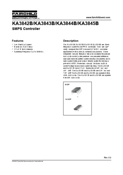
The KA3842A-BW/43A-BW/44A-BW/45A-BW,KA 3842M/43M/44M/45M are fixed frequency current mode PWM controller. They are specially designed for OFF−Line and DC to DC
12
13.0
45
150
35
150
Undervoltage Lockout Section
Start Theshold
VTH(ST)
KA3842A-BW/44A-BW/42M/44M
14.5
16.0
17.5
Min. Operating Voltage
VOPR(min) KA3842A-BW/44A-BW/42M/44M
voltage lockout and current limiting.
The KA3842A-BW, KA3844A-BW, KA3842M and KA 3844M have UVLO thresholds of