超大规模集成电路2017年秋段成华老师第四次作业
- 格式:doc
- 大小:247.09 KB
- 文档页数:9

浙江省舟山市2022-2023学年金衢山五校联盟校八年级第一学期12月月考科学试题卷注意事项:1.本试题卷分卷I(选择题)和卷II(非选择题)两部分。
考试时间120分钟。
2.本卷共有10页,4大题,35小题,满分为180分。
3.本卷答案必须做在答题卷的相应位置上,做在试卷上无效。
4.g取10牛/千克第I卷(选择题)一、选择题(本题有15小题,第1-10小题,每小题3分;第11-15小题,每小题4分,共50分。
请选出各题中一个符合题意的正确选项,不选、多选、错选,均不给分)1.水是人类不可缺少的宝贵资源,以下是我国“节水标志”的是()A.B.C.D.2.下列有关粗盐提纯的各个步骤,操作规范的是()A.取粗盐B.溶解C.过滤D.蒸发结晶3.如图所示电路中,开关不能同时控制两盏灯的是()A.B.C.D.4.下列四种情景都与气压有关,只有一种情景与其他三种的原理不同,这种情景是()A.刮大风时,玻璃钢瓦的屋B.等候列车的乘客应站在安全线以外,顶被大风“掀”起否则会被“吸”向列车C.打开的窗户外有平行于墙壁的D.将吸盘按压在光洁的瓷砖表面,风吹过时,窗帘会“飘”出窗外放手后吸盘会被“吸”在瓷砖上5.下图表示先天性行为与学习行为的相同点和不同点,其中阴影部分表示相同点。
下列哪一项可以写在阴影部分( )A.与生俱有B.由生活经验和学习获得C.有利于生存和繁殖D.能伴随动物一生6.下列是有关科学问题中的因果关系,其中说法正确的是( )A.浮在水面上的铁球一定是空心的,那么空心的铁球一定会浮在水面上B.溶液是均一的,稳定的,那么均一的,稳定的物质一定是溶液C.饱和溶液恒温蒸发后有固体析出,那么能恒温蒸发析出固体的溶液一定是饱和溶液D.密度比液体小的固体漂浮在液体中,那么漂浮在该液体中的实心固体的密度一定比液体小7.如图所示,两端开口的气缸水平固定,A、B是两个厚度不计的活塞,可在气缸内无摩擦滑动,面积分别为S1=20cm2,S2=10cm2,它们之间用一根细杆连接,B通过水平细绳绕过光滑的定滑轮与质量为M=2kg的重物C连接,活塞的初始状态为静止,已知大气压强P0=1×10⁵Pa,取g=10N/kg,下列说法不正确的是()A.活塞初始静止时,活塞A受到细杆的作用力水平向右B.活塞初始静止时,气缸内压强为1.2×103PaC.若升高气缸内气体温度,活塞B向左移动D.若降低缸内气体温度10℃,活塞运动-段距离L就停止,停止时气缸内压强比初始状态时气缸压强要小8.计算机运行的基础是集成电路,超大规模集成电路是指在在一块极小的芯片上集成的元件数超过10万个,或门电路数超过万门的集成电路,主要用于计算机制造存储器和微处理机。
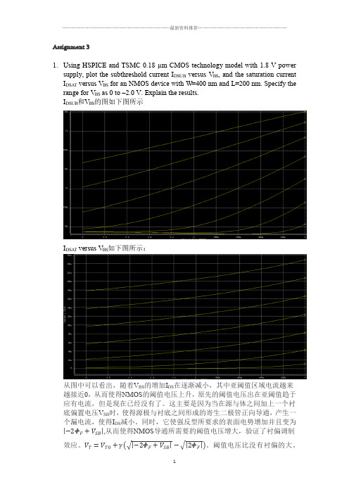
Assignment 3ing HSPICE and TSMC 0.18 µm CMOS technology model with 1.8 V powersupply, plot the subthreshold current I DSUB versus V BS, and the saturation currentI DSAT versus V BS for an NMOS device with W=400 nm and L=200 nm. Specify therange for V BS as 0 to –2.0 V. Explain the results.I DSUB和V BS的图如下图所示I DSAT versus V BS如下图所示:从图中可以看出,随着V BS的增加I DS在逐渐减小,其中亚阈值区域电流越来越接近0,从而使得NMOS的阈值电压上升,原先的阈值电压出在亚阈值趋于应有电流,但是现在已经没有了。
这主要是因为当在源与体之间加上一个衬底偏置电压V SB时,使得源极与衬底之间形成的寄生二极管正向导通,产生一个漏电流,使得I DS减小。
同时,它使强反型所要求的表面电势增加并且变为,从而使得NMOS导通所需要的阈值电压增大,验证了衬偏调制效应。
阈值电压比没有衬偏的大。
* SPICE INPUT FILE: problem.sp ID-VBS.param Supply=1.8 * Set value of Vdd.lib 'C:\synopsys\Hspice_A-2007.09\tsmc018\mm018.l' TT * Set 0.18um library .opt scale=0.1u * Set lambda*.model pch PMOS level=49 version=3.1*.model nch NMOS level=49 version=3.1mn Vdd gaten Gnd bn nch l=2 w=4 ad=20 pd=4 as=20 ps=4Vdd Vdd 0 'Supply'Vgsn gaten Gnd d cVbsn bn Gnd d c.dc Vbsn 0 -2 -0.05 Vgsn 0.6 1.8 0.2.print dc I1(mn).ending HSPICE and TSMC 0.18 um CMOS technology model with 1.8 V powersupply, plot log I DS versus V GS while varying V DS for an NMOS device withL=200 nm, W=800 nm and a PMOS with L=200 nm, W= 2 µm. Explain theresults.图中红线表示NMOS的I DS对V GS的曲线,从图中可以看出,随着V GS的增大I DS 的电流先为0,到后来逐渐增大,最后I DS对V GS的关系接近一个线性变化,且NMOS的导通电压约为0.43V,当V GS=0.43V的时候NMOS导通。
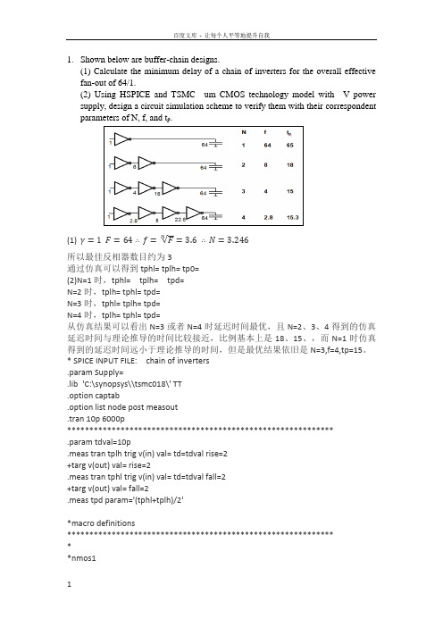
1.Shown below are buffer-chain designs.(1) Calculate the minimum delay of a chain of inverters for the overall effectivefan-out of 64/1.(2) Using HSPICE and TSMC um CMOS technology model with V powersupply, design a circuit simulation scheme to verify them with their correspondent parameters of N, f, and t p.N=3.6 ∴N=3.246(1)γ=1 F=64∴f=√F所以最佳反相器数目约为3通过仿真可以得到tphl= tplh= tp0=(2)N=1时,tphl= tplh= tpd=N=2时,tplh= tphl= tpd=N=3时,tphl= tplh= tpd=N=4时,tplh= tphl= tpd=从仿真结果可以看出N=3或者N=4时延迟时间最优,且N=2、3、4得到的仿真延迟时间与理论推导的时间比较接近,比例基本上是18、15、,而N=1时仿真得到的延迟时间远小于理论推导的时间,但是最优结果依旧是N=3,f=4,tp=15。
* SPICE INPUT FILE: chain of inverters.param Supply=.lib 'C:\synopsys\\tsmc018\' TT.option captab.option list node post measout.tran 10p 6000p************************************************************.param tdval=10p.meas tran tplh trig v(in) val= td=tdval rise=2+targ v(out) val= rise=2.meas tran tphl trig v(in) val= td=tdval fall=2+targ v(out) val= fall=2.meas tpd param='(tphl+tplh)/2'*macro definitions**************************************************************nmos1.subckt nmos1 n1 n2 n3mn n1 n2 n3 Gnd nch l= w= ad=^2 pd= as=^2 ps= .ends nmos1**pmos1*.subckt pmos1 p1 p2 p3mp p1 p2 p3 Vcc pch l= w= ad=^2 pd= as=^2 ps= .ends pmos1*.subckt inv1 in outxmn out in Gnd nmos1xmp out in Vcc pmos1vcc Vcc Gnd Supply.ends inv1**nmos2*.subckt nmos2 n1 n2 n3mn n1 n2 n3 Gnd nch l= w= ad=^2 pd= as=^2 ps= .ends nmos2**pmos2*.subckt pmos2 p1 p2 p3mp p1 p2 p3 Vcc pch l= w= ad=^2 pd= as=^2 ps= .ends pmos2*.subckt inv2 in outxmn out in Gnd nmos2xmp out in Vcc pmos2vcc Vcc Gnd Supply.ends inv2**nmos3*.subckt nmos3 n1 n2 n3mn n1 n2 n3 Gnd nch l= w= ad=^2 pd= as=^2 ps= .ends nmos3**pmos3.subckt pmos3 p1 p2 p3mp p1 p2 p3 Vcc pch l= w= ad=^2 pd= as=^2 ps=.ends pmos3*.subckt inv3 in outxmn out in Gnd nmos3xmp out in Vcc pmos3vcc Vcc Gnd Supply.ends inv3**nmos4*.subckt nmos4 n1 n2 n3mn n1 n2 n3 Gnd nch l= w= ad=^2 pd= as=^2 ps=.ends nmos4**pmos4*.subckt pmos4 p1 p2 p3mp p1 p2 p3 Vcc pch l= w= ad=^2 pd= as=^2 ps=.ends pmos4*.subckt inv4 in outxmn out in Gnd nmos4xmp out in Vcc pmos4vcc Vcc Gnd Supply.ends inv4*main circuit netlistxinv1 in out1 inv1xinv2 out1 out2 inv2xinv3 out2 out3 inv3xinv4 out3 out inv4cl out GndVin in Gnd pulse 219p 40p 40p 1100p 2400p).print tran v(in) v(out).end2.Consider the logic network below, which may represent the critical path of a morecomplex logic block. The output of the。
超大规模集成电路第九次作业2016秋-段成华-CAL-FENGHAI.-(YICAI)-Company One1Assignment 91. Design an 8-bit up and down synchronous counter in VHDL with the following features:(1)The same ports are used for signals to be inputted andoutputted. The ports are bi-directionally buffered (three-state).(2)The counter is with an asynchronous reset that assigns aspecific initial value for counting.(3)The counter is with a synchronous data load control input fora new value of counting and an enable control input forallowing the up and down counting. The load control input hasa priority over the enable control input. This implies thatwhen the load operation is in process the counter operation is prohibited.(4)Some data types, such as STD_LOGIC, UNSIGNED, SIGNED andINTEGER, may be used.Synthesize the design. Create a set of reasonable input waveforms for your design and complete both behavioral and post-place&route simulations with internal signals and/or variables included in waveform or list windows.Solution:代码如下:library IEEE;use IEEE.STD_LOGIC_1164.ALL;use IEEE.STD_LOGIC_ARITH.ALL;use IEEE.STD_LOGIC_UNSIGNED.ALL;---- Uncomment the following library declaration if instantiating---- any Xilinx primitives in this code.--library UNISIM;--use UNISIM.VComponents.all;entity count_8_bidir isPort (clk : in STD_LOGIC;rst : in STD_LOGIC;load : in STD_LOGIC;enable : in STD_LOGIC;cnt : inout STD_LOGIC_VECTOR (7 downto 0));end count_8_bidir;architecture Behavioral of count_8_bidir issignal cnt_in: STD_LOGIC_VECTOR (7 downto 0);signal cnt_out: STD_LOGIC_VECTOR (7 downto 0);beginpro0:process(oe,cnt_out,cnt)beginif(load='1')thencnt <= (others=>'Z');cnt_in <= cnt;elsecnt <= cnt_out;end if;end process;pro1:process(clk,rst)beginif(rst='1')thencnt_out <= (others=>'0');elsif rising_edge(clk)thenif(load='1')thencnt_out <= cnt_in;elsif(enable='1')thencnt_out <=cnt_out + 1;elsecnt_out <= cnt_out - 1;end if;end if;end process;end Behavioral;解释代码:这里有两个进程,进程0时是用来控制三态门控制的双向端口。

超大规模集成电路2017年秋段成华老师第三次作业(总6页)--本页仅作为文档封面,使用时请直接删除即可----内页可以根据需求调整合适字体及大小--Assignment 3ing HSPICE and TSMC µm CMOS technology model with V power supply,plot the subthreshold current I DSUB versus V BS, and the saturation current I DSATversus V BS for an NMOS device with W=400 nm and L=200 nm. Specify the range for V BS as 0 to – V. Explain the results.I DSUB和V BS的图如下图所示I DSAT versus V BS如下图所示:从图中可以看出,随着V BS的增加I DS在逐渐减小,其中亚阈值区域电流越来越接近0,从而使得NMOS的阈值电压上升,原先的阈值电压出在亚阈值趋于应有电流,但是现在已经没有了。
这主要是因为当在源与体之间加上一个衬底偏置电压V SB时,使得源极与衬底之间形成的寄生二极管正向导通,产生一个漏电流,使得I DS减小。
同时,它使强反型所要求的表面电势增加并且变为|−2ΦF+V SB|,从而使得NMOS导通所需要的阈值电压增大,验证了衬偏调制效应。
V T=V T0+γ(√|−2ΦF+V SB|−√|2ΦF|)。
阈值电压比没有衬偏的大。
* SPICE INPUT FILE: ID-VBS.param Supply= * Set value of Vdd.lib 'C:\synopsys\\tsmc018\' TT * Set library.opt scale= * Set lambda*.model pch PMOS level=49 version=*.model nch NMOS level=49 version=mn Vdd gaten Gnd bn nch l=2 w=4 ad=20 pd=4 as=20 ps=4Vdd Vdd 0 'Supply'Vgsn gaten Gnd dcVbsn bn Gnd dc.dc Vbsn 0 -2 Vgsn.print dc I1(mn).ending HSPICE and TSMC um CMOS technology model with V power supply,plot log I DS versus V GS while varying V DS for an NMOS device with L=200 nm, W=800 nm and a PMOS with L=200 nm, W= 2 µm. Explain the results.图中红线表示NMOS的I DS对V GS的曲线,从图中可以看出,随着V GS的增大I DS的电流先为0,到后来逐渐增大,最后I DS对V GS的关系接近一个线性变化,且NMOS的导通电压约为,当V GS=的时候NMOS导通。
无锡市专业技术人员继续教育公修课《现代高新科技及其产业发展》模拟试卷四本试卷共6页1.引进消化吸收再创新的办法只能是一时的,( )才是根本。
A.集成创新B.原始创新C.引进消化吸收再创新D.自主创新2.2004年我国科技创新能力在49个主要国家中位居第( )位。
A.30B.14C.24D.33.( )年,我国正式批准建设高新技术开发区。
A.1988B.2000C.1993D.19914.( )是我国自主研发的第三代移动通信国际技术标准,是我国在自主创新领域的重要实践和典范。
A.IPV6B.TD-SCDMAC.WCDMAD.CDMA20005.光计算机的运算速度至少比现在的计算机快( ),高达一万亿次,存储容量比现在的计算机大百万倍。
A.10倍 B.100倍 C.1000倍 D.10000倍6.超大规模集成电路是指集成( )晶体管的集成电路。
A.100~1000个B.1000个以上C.10万以上D.1000万以上7.金属的超塑性现象是英国物理学家()在1982年发现的。
A.科勒 B.森金斯 C.基尔比 D.米尔斯坦8.人工合成的有机高分子材料中,()诞生最早,发展最快。
A.塑料 B.橡胶 C.合成纤维 D.涂料9.()电池是目前性能最好的电池体系。
A.镍氢电池 B.镍锌电池 C.金属空气电池 D.锂离子电池10.全世界石油产量中,将近()来自海底。
A.60% B.10% C.30% D.80%11.被誉为第四次科技革命浪潮的是()A.农业经济B.工业经济C.生物经济D.信息经济12.我国人类基因组计划启动于()A.1990年B.1991年C.1992年D.1993年13.植物组织培养技术中最成熟、应用最广泛的是()A.植物微繁殖技术B.单倍体细胞培养技术C.体细胞无性系变异技术D.种质保存技术14.我国农业科研经费占农业总产值的()A.2%—4%B.1%C.0.2%—0.5%D.0.1%—0.2%15.最早提出“环境科学”这一名词的学者是()A.美国人B.英国人C.日本人D.德国人二、多项选择题(每题2分,共30分。
二级MS OFFICE高级应用-17-1(总分100, 做题时间90分钟)选择题下列各题A、B、D、D四个选项中,只有一个选项是正确的。
1.按电子计算机传统的分代方法,第一代至第四代计算机依次是______。
• A.机械计算机,电子管计算机,晶体管计算机,集成电路计算机• B.晶体管计算机,集成电路计算机,大规模集成电路计算机,光器件计算机• C.电子管计算机,晶体管计算机,中小规模集成电路计算机,大规模和超大规模集成电路计算机• D.手摇机械计算机,电动机械计算机,电子管计算机,晶体管计算机SSS_SIMPLE_SINA B C D该问题分值: 2.5答案:C[解析] 计算机于1946年问世以来,经过了四个重要的历史阶段。
第一代是电子管计算机(1945—1956年),它的特点是采用电子管作为原件。
第二代是晶体管计算机(1956—1963年),晶体管代替了体积庞大的电子管,电子设备的体积不断减小。
第三代是中小规模集成电路计算机(1964—1971年),使更多的元件集成到单一的半导体芯片上。
计算机变得更小,功耗更低,速度更快。
第四代是大规模集成电路计算机(1971—现在),其最显著特点是大规模集成电路和超大规模集成电路的运用。
2.假设某台式计算机的内存储器容量为256MB,硬盘容量为40GB。
硬盘容量是内存容量的______。
•**倍•**倍•**倍**倍SSS_SIMPLE_SINA B C D该问题分值: 2.5答案:B[解析] 计算机存储器容量都是以字节为单位表示的。
除用字节为单位表示存储容量外,还可以用(KB)、(MB)以及(GB)等表示存储容量。
它们之间的换算关系如下:1B=8bit;1KB=210B=1024B;1MB=220B=1024KB;1GB=230B=1024MB。
3.在ASCII编码表中,根据码值由小到大的排列顺序是______。
• A.空格字符、数字符、大写英文字母、小写英文字母• B.数字符、空格字符、大写英文字母、小写英文字母• C.空格字符、数字符、小写英文字母、大写英文字母• D.数字符、大写英文字母、小写英文字母、空格字符SSS_SIMPLE_SINA B C D该问题分值: 2.5答案:A[解析] 标准ASCII码表用七位二进制表示一个字符(或用一个字节表示,最高位为“0”)表示128个不同的字符。
《超大规模数字集成电路》试题B第 1 页共 2 页内蒙古科技大学2015/2016学年第二学期《超大规模数字集成电路》考试试题B课程号:671180800考试方式:闭卷使用专业、年级:电子信息工程、通信工程2013 任课教师:侯海鹏考试时间:2016年9月备注:一、选择题(共12题,每题2分,共24分)1.下面()不是硅材料在集成电路技术中起着举足轻重的作用的原因。
(A) 原材料来源丰富 (B) 技术成熟 (C) 价格低廉 (D) 硬度高2.下面()不是芯片电感的实现结构。
(A) 匝线圈 (B) 叉指金属结构 (C) 螺旋形多匝线圈 (D) 传输线结构3.P,Q,R 都是4bit 的输入矢量,下面()的表达形式是正确的。
(A)input [3:0]P,[3:0]Q,[0:3]R; (B) input P,Q,R[3:0]; (C) input P[3:0],Q[3:0],R[3:0]; (D) input [3:0] P,Q,R; 4.根据以下两条语句,下列选项中()是正确的。
reg [7:0] B; B=8'bZ0;(A) 8'0000_00Z0 (B) 8'bZZZZ_0000 (C) 8'b0000_ZZZ0 (D) 8'bZZZZ_ZZZ0 5.在Verilog HDL 中,下列语句中()不是分支语句。
(A) if-else (B) case(C) casez(D) repeat6.在下列标识符中,()是不合法的标识符。
(A) 9moon(B) State0(C) Not_Ack_0 (D) signall7.Verilog HDL 中并行块语句的关键字是()(A) module…endmoudle (B) begin …end (C) fork …join (D) if …else 8.已知“a =1b ’1; b=3b’100;”那么{a,b}=()(A)4b ’0100(B) 3b ’110(C) 4b ’1100(D) 3b ’1009.在下列表达式中,正确的是()。
《超大规模集成电路设计》习题1.集成电路的发展过程经历了哪些发展阶段?划分集成电路的标准是什么?集成电路的发展过程:•小规模集成电路(Small Scale IC,SSI)•中规模集成电路(Medium Scale IC,MSI)•大规模集成电路(Large Scale IC,LSI)•超大规模集成电路(Very Large Scale IC,VLSI)•特大规模集成电路(Ultra Large Scale IC,ULSI)•巨大规模集成电路(Gigantic Scale IC,GSI)划分集成电路规模的标准2.超大规模集成电路有哪些优点?1. 降低生产成本VLSI减少了体积和重量等,可靠性成万倍提高,功耗成万倍减少.2.提高工作速度VLSI内部连线很短,缩短了延迟时间.加工的技术越来越精细.电路工作速度的提高,主要是依靠减少尺寸获得.3. 降低功耗芯片内部电路尺寸小,连线短,分布电容小,驱动电路所需的功率下降.4. 简化逻辑电路芯片内部电路受干扰小,电路可简化.5.优越的可靠性采用VLSI后,元件数目和外部的接触点都大为减少,可靠性得到很大提高。
6.体积小重量轻7.缩短电子产品的设计和组装周期一片VLSI组件可以代替大量的元器件,组装工作极大的节省,生产线被压缩,加快了生产速度.3.简述双阱CMOS工艺制作CMOS反相器的工艺流程过程。
4.在VLSI设计中,对互连线的要求和可能的互连线材料是什么?5.在进行版图设计时为什么要制定版图设计规则?在芯片尺寸尽可能小的前提下,使得即使存在工艺偏差也可以正确的制造出IC,尽可能地提高电路制备的成品率6.版图验证和检查主要包括哪些方面?◆DRC(Design Rule Check):几何设计规则检查;对IC的版图做几何空间检查,保证能在特定的工艺条件下实现所设计的电路,并保证一定的成品率;◆ ERC(Electrical Rule Check):电学规则检查;检查电源(power)/地(ground)的短路,浮空的器件和浮空的连线等指定的电气特性;◆ LVS(Loyout versus Schematic):网表一致性检查;将版图提出的网表和原理图的网表进行比较,检查电路连接关系是否正确,MOS晶体管的长/宽尺寸是否匹配,电阻/电容值是否正确等;◆LPE(Layout Parameter Extraction):版图寄生参数提取;从版图中提取晶体管的尺寸、结点的寄生电容、连线的寄生电阻等参数,并产生SPICE 格式的网表,用于后仿真验证;◆ POSTSIM:后仿真,检查版图寄生参数对设计的影响;提取实际版图参数、电阻、电容,生成带寄生量的器件级网表,进行开关级逻辑模拟或电路模拟,以验证设计出的电路功能的正确性和时序性能等,并产生测试向量。
1.Shown below are buffer-chain designs.(1) Calculate the minimum delay of a chain of inverters for the overalleffective fan-out of 64/1.(2) Using HSPICE and TSMC 0.18 um CMOS technology model with 1.8 V powersupply, design a circuit simulation scheme to verify them with their.correspondent parameters of N, f, and tpN=3.6 ∴N=3.246(1)γ=1 F=64∴f=√F所以最佳反相器数目约为3通过仿真可以得到tphl=1.3568E-11 tplh=1.7498E-11 tp0=1.5533E-11(2)N=1时,tphl= 5.2735E-10 tplh= 8.1605E-10 tpd= 6.7170E-10N=2时,tplh=2.2478E-10 tphl=2.5567E-10 tpd=2.4023E-10N=3时,tphl=2.0574E-10 tplh=2.1781E-10 tpd=2.1178E-10N=4时,tplh=2.1579E-10 tphl=2.2189E-10 tpd=2.1884E-10从仿真结果可以看出N=3或者N=4时延迟时间最优,且N=2、3、4得到的仿真延迟时间与理论推导的时间比较接近,比例基本上是18、15、15.3,而N=1时仿真得到的延迟时间远小于理论推导的时间,但是最优结果依旧是N=3,f=4,tp=15。
* SPICE INPUT FILE: Bsim3demo1.sp--a chain of inverters.param Supply=1.8.lib 'C:\synopsys\Hspice_A-2007.09\tsmc018\mm018.l' TT.option captab.option list node post measout.tran 10p 6000p************************************************************.param tdval=10p.meas tran tplh trig v(in) val=0.9 td=tdval rise=2+targ v(out) val=0.9 rise=2.meas tran tphl trig v(in) val=0.9 td=tdval fall=2+targ v(out) val=0.9 fall=2.meas tpd param='(tphl+tplh)/2'*macro definitions**************************************************************nmos1.subckt nmos1 n1 n2 n3mn n1 n2 n3 Gnd nch l=0.2u w=0.4u ad=0.2p^2 pd=0.4u as=0.2p^2 ps=0.4u .ends nmos1**pmos1*.subckt pmos1 p1 p2 p3mp p1 p2 p3 Vcc pch l=0.2u w=0.8u ad=0.4p^2 pd=0.8u as=0.4p^2 ps=0.8u .ends pmos1*.subckt inv1 in outxmn out in Gnd nmos1xmp out in Vcc pmos1vcc Vcc Gnd Supply.ends inv1**nmos2*.subckt nmos2 n1 n2 n3mn n1 n2 n3 Gnd nch l=0.2u w=1.12u ad=0.56p^2 pd=1.12u as=0.56p^2 ps=1.12u .ends nmos2**pmos2*.subckt pmos2 p1 p2 p3mp p1 p2 p3 Vcc pch l=0.2u w=2.24u ad=1.12p^2 pd=2.24u as=1.12p^2 ps=2.24u .ends pmos2*.subckt inv2 in outxmn out in Gnd nmos2xmp out in Vcc pmos2vcc Vcc Gnd Supply.ends inv2**nmos3*.subckt nmos3 n1 n2 n3mn n1 n2 n3 Gnd nch l=0.2u w=3.2u ad=1.6p^2 pd=3.2u as=1.6p^2 ps=3.2u .ends nmos3**pmos3.subckt pmos3 p1 p2 p3mp p1 p2 p3 Vcc pch l=0.2u w=6.4u ad=3.2p^2 pd=6.4u as=3.2p^2 ps=6.4u .ends pmos3*.subckt inv3 in outxmn out in Gnd nmos3xmp out in Vcc pmos3vcc Vcc Gnd Supply.ends inv3**nmos4*.subckt nmos4 n1 n2 n3mn n1 n2 n3 Gnd nch l=0.2u w=9.04u ad=4.52p^2 pd=9.04u as=4.52p^2 ps=9.04u .ends nmos4**pmos4*.subckt pmos4 p1 p2 p3mp p1 p2 p3 Vcc pch l=0.2u w=18.08u ad=9.04p^2 pd=18.08u as=9.04p^2 ps=18.08u.ends pmos4*.subckt inv4 in outxmn out in Gnd nmos4xmp out in Vcc pmos4vcc Vcc Gnd Supply.ends inv4*main circuit netlistxinv1 in out1 inv1xinv2 out1 out2 inv2xinv3 out2 out3 inv3xinv4 out3 out inv4cl out Gnd 154.24fVin in Gnd 0.9 pulse(0.0 1.8 219p 40p 40p 1100p 2400p).print tran v(in) v(out).end2.Consider the logic network below, which may represent the critical pathof a more complex logic block. The output of the。
network is loaded with a capacitance which is 5 times larger than the input capacitanceof the first gate, which is a minimum-sized inverter. The effective fanout of the path hence equals F = CL/Cg1 = 5.Using HSPICE and TSMC 0.18 um CMOS technology model with 1.8 V power supply, design a circuit simulation scheme to verify(1) the OPTIMAZATIOM parameters of g, f, and s for each of the inverter and gates andThe path logical effort G=1∗53∗53∗1=259The total path effort H=GFB=259∗5∗1=1259The optimal gate effort h=H14⁄=(1259)⁄14⁄=1.93f1g1=f2g2=f3g3=f4g4=1.93g1=1 g2=53⁄ g3=53⁄ g4=1f1=1.93 f2=1.16 f3=1.16 f4=1.93s1=1 s2=1.16 s3=1.34 s4=2.6在所有的nmos和pmos均采用最小尺寸晶体管的情况下tplh=1.9047E-10 tphl=2.2742E-10 tpd=2.0895E-10在所有所有的mos管尺寸均是前一个mos管尺寸的2倍的情况下tplh=1.8353E-10 tphl=2.4356E-10 tpd=2.1355E-10在参数最优的情况下tplh= 1.7151E-10 tphl=2.2853E-10 tpd=2.0002E-10所以最优参数为上面的推到过程。
* SPICE INPUT FILE: Bsim3demo1.sp--a chain of inverters.param Supply=1.8.lib 'C:\synopsys\Hspice_A-2007.09\tsmc018\mm018.l' TT.option captab.option list node post measout.tran 10p 6000p************************************************************.param tdval=10p.meas tran tplh trig v(in) val=0.9 td=tdval rise=2+targ v(out) val=0.9 rise=2.meas tran tphl trig v(in) val=0.9 td=tdval fall=2+targ v(out) val=0.9 fall=2.meas tpd param='(tphl+tplh)/2'*macro definitions**************************************************************nmos1*.subckt nmos1 n1 n2 n3mn n1 n2 n3 Gnd nch l=0.2u w=0.4u ad=0.2p^2 pd=0.4u as=0.2p^2 ps=0.4u.ends nmos1**pmos1*.subckt pmos1 p1 p2 p3mp p1 p2 p3 Vcc pch l=0.2u w=0.8u ad=0.4p^2 pd=0.8u as=0.4p^2 ps=0.8u.ends pmos1*.subckt inv1 in outxmn out in Gnd nmos1xmp out in Vcc pmos1vcc Vcc Gnd Supply.ends inv1**nmos2*.subckt nmos2 n1 n2 n3 n4mn n1 n2 n3 n4 nch l=0.2u w=0.772u ad=0.386p^2 pd=0.772u as=0.386p^2 ps=0.772u.ends nmos2**pmos2*.subckt pmos2 p1 p2 p3 p4mp p1 p2 p3 p4 pch l=0.2u w=1.544u ad=0.772p^2 pd=1.544u as=0.772p^2 ps=1.544u.ends pmos2*.subckt nand in1 in2 in3 outxmn1 d1 in1 Gnd Gnd nmos2xmn2 d2 in2 d1 d1 nmos2xmn3 out in3 d2 d2 nmos2xmp1 out in1 Vcc Vcc pmos2xmp2 out in2 Vcc Vcc pmos2xmp3 out in3 Vcc Vcc pmos2vcc Vcc Gnd Supply**nmos3*.subckt nmos3 n1 n2 n3 n4mn n1 n2 n3 n4 nch l=0.2u w=0.9u ad=0.45p^2 pd=0.9u as=0.45p^2 ps=0.9u.ends nmos3**pmos3*.subckt pmos3 p1 p2 p3 p4mp p1 p2 p3 p4 pch l=0.2u w=1.79u ad=0.895p^2 pd=1.79u as=0.895p^2 ps=1.79u.ends pmos3*.subckt nor in1 in2 outxmn1 out in1 Gnd Gnd nmos3xmn2 out in2 Gnd Gnd nmos3xmp1 out in1 d1 d1 pmos3xmp2 d1 in2 Vcc Vcc pmos3vcc Vcc Gnd Supply.ends nor**nmos4*.subckt nmos4 n1 n2 n3mn n1 n2 n3 Gnd nch l=0.2u w=1.044u ad=0.522p^2 pd=1.044u as=0.522p^2 ps=1.044u.ends nmos4**pmos4*.subckt pmos4 p1 p2 p3mp p1 p2 p3 Vcc pch l=0.2u w=2.0764u ad=1.0382p^2 pd=2.0764u as=1.0382p^2 ps=2.0764u.ends pmos4*.subckt inv2 in outxmn out in Gnd nmos4xmp out in Vcc pmos4vcc Vcc Gnd Supply*main circuit netlistxinv1 in out1 inv1xnand out1 Vcc Vcc out2 nandxnor out2 Gnd out3 norxinv2 out3 out inv2cl out Gnd 12.05fvcc Vcc Gnd SupplyVin in Gnd 0.9 pulse(0.0 1.8 219p 40p 40p 1100p 2400p).print tran v(in) v(out).end(2) the minimum delay of the chain.在参数最优的情况下tplh= 1.7151E-10 tphl=2.2853E-10 tpd=2.0002E-103.Shown below is a level restore circuit of pass transistor.(1) Without trans3istor M r,4 verify by using HSPICE and TSMC 0.18 umCMOS technology model with 1.8 V power supply that the high input to the signal- restoring inverter only charges up to V DD - V Tn.=0.445V,所以V x≈1.8V−0.445V≈通过仿真,我们得到V(x)=1.38V,VTnV DD−V Tn,无法达到VDD的最大值1.8V。