PSA05-12SRWA, 规格书,Datasheet 资料
- 格式:pdf
- 大小:248.36 KB
- 文档页数:6

SURFACE MOUNT SCHOTTKY BARRIER RECTIFIERFeatures• Low Forward Voltage Drop• Guard Ring Construction for Transient Protection • High Conductance• Lead Free By Design/RoHS Compliant (Note 3) • "Green" Device (Note 4)Mechanical Data• Case: SOD-323• Case Material: Molded Plastic, "Green" Molding Compound.UL Flammability Rating Classification 94V-0• Moisture Sensitivity: Level 1 per J-STD-020D• Polarity: Cathode Band• Terminals: Finish - Matte Tin Annealed Over Alloy 42leadframe. Solderable per MIL-STD-202, Method 208 • Marking Information: See Page 2• Ordering Information: See Page 2• Weight: 0.004 grams (approximate)Top ViewMaximum Ratings@T A = 25°C unless otherwise specifiedSingle phase, half wave, 60Hz, resistive or inductive load.For capacitance load, derate current by 20%.Characteristic Symbol Value UnitPeak Repetitive Reverse Voltage Working Peak Reverse Voltage DC Blocking Voltage V RRMV RWMV R40 VRMS Reverse Voltage V R(RMS)28 V Average Rectified Output Current I O0.5 ANon-Repetitive Peak Forward Surge Current8.3ms single half sine-wave superimposed on rated load I FSM3 A Thermal CharacteristicsCharacteristic Symbol Value Unit Power Dissipation (Note 1) P D235 mW Typical Thermal Resistance Junction to Ambient (Note 1) RθJA426 °C/W Operating and Storage Temperature Range T J, T STG-40 to +125 °CElectrical Characteristics@T A = 25°C unless otherwise specifiedCharacteristic Symbol Min Typ Max Unit Test Condition Reverse Breakdown Voltage (Note 2) V(BR)R40 ⎯⎯V I R = 1mAForward Voltage V F⎯285480300550mVI F = 10mAI F = 500mAReverse Current (Note 2) I R ⎯⎯1.02.035μAμAV R = 10VV R = 30VTotal Capacitance C T ⎯⎯12520⎯⎯pFpFV R = 0V, f = 1.0MHzV R = 10V, f = 1.0MHzNotes: 1. Part mounted on FR-4 PC board with recommended pad layout, which can be found on our website at /datasheets/ap02001.pdf.2. Short duration pulse test used to minimize self-heating effect.3. No purposefully added Lead.4. Diodes Inc.'s "Green" policy can be found on our website at /products/lead_free/index.php.Please click here to visit our online spice models database.10100V, INSTANTANEOUS REVERSE VOLTAGE (V)Fig. 2 Typical Reverse CharacteristicsRI,INSTANTANEOUSFORWARDCURRENT(mA)FV, INSTANTANEOUS FORWARD VOLTAGE (V)Fig. 1 Typical Forward CharacteristicsF100C,TOTALCAPACITANCE(pF)TV, DC REVERSE VOLTAGE (V)Fig. 3 Total Capacitance vs. Reverse VoltageR0.250.50050100I,AVE150RAGEFORWARDCURRENT(A)F(AV)T, TERMINAL TEMPERATURE (C)Fig. 4 Forward Current Derating CurveT°0.751.02575125Ordering Information(Note 5)Part Number Case PackagingB0540WS-7 SOD-323 3000/Tape & ReelNotes: 5. For packaging details, go to our website at /datasheets/ap02007.pdf.Marking InformationSF SF = Product Type Marking CodePackage Outline DimensionsSuggested Pad LayoutIMPORTANT NOTICEDiodes Incorporated and its subsidiaries reserve the right to make modifications, enhancements, improvements, corrections or other changes without further notice to any product herein. Diodes Incorporated does not assume any liability arising out of the application or use of any product described herein; neither does it convey any license under its patent rights, nor the rights of others. The user of products in such applications shall assume all risks of such use and will agree to hold Diodes Incorporated and all the companies whose products are represented on our website, harmless against all damages.LIFE SUPPORTDiodes Incorporated products are not authorized for use as critical components in life support devices or systems without the expressed written approval of the President of Diodes Incorporated.SOD-323 Dim Min Max A 0.25 0.35 B 1.20 1.40 C 2.30 2.70 H 1.60 1.80 J 0.00 0.10 K 1.0 1.1 L0.20 0.40 M 0.10 0.15α0° 8°All Dimensions in mmDimensions Value (in mm)Z 3.75 G 1.05 X 0.65 Y 1.35 C 2.40分销商库存信息: DIODESB0540WS-7。

PS-002-004012016-7-28客户名/CustomerRELAY SPECIFICATION零件编号/Part Number品名/Product Description RJ-SS-112DM1-SDate Version PS No.继 电 器 规 格 书冯旭强余明亮王凤客户批准/Customer Approval 盖章处/STAMPING AREAR&DSM PD发行批准 / Issued by序号担当00凌剑冰01凌剑冰2016-7-28增加黄山工厂描述变更履历/HISTORY日期变更项目2015-4-13初版1零件清单/PARTS LIST123 4 5 6 7 8 9 10 11 12 13 14 15 16Ver01RG3015010GN6-30 M8XRG301RG301FLAME CLASSUL FILE No.E171666E53664E171666E171666TYPE/TREATMENT型号/处理方式镀镍Vicryst R850Part零件名No.材质MATERIAL镀镍Nickel Plated镀镍Nickel PlatedNickel Plated3UEW 155(F Class)镀锡Base基座骨架Bobbin外壳Case推片CardSolder Coated挂钩Hinge可动弹片C Terminal轭铁Yoke衔铁Armature线材Wire可动接点C ContactM接点M ContactE171666线圈端子Coil Terminal铁芯CoreM端子M TerminalE234867PS-002-004E164502Epoxy胶水UV GlueSealing ResinAg Alloy铜包钢Cu coverd Steel聚氨脂漆包圆铜线Cu Alloy铜合金Polyurethane copper wire环氧树脂Steel铜合金Cu Alloy银合金Ag Alloy银合金Cu Alloy铁LCP铁Steel铁Steel铜合金PBTUV胶PBTPBT2.性能/SPECIFICATIONS2.1驱动部分/COIL SPECIFICATIONS2.1.1额定电压12VDC(在20℃时)Rated Coil Voltage12VDC at 20℃2.1.2额定功率0.45W(在20℃时)Nominal Power0.45W at 20℃2.1.3线圈电阻320Ω±10%(在20℃时)Coil Resistance320Ω±10%(at 20℃)2.1.4额定电流37.5mA±10%(在20℃时)Nominal Current37.5mA±10%(at 20℃)2.1.5吸合电压9VDC以下(在20℃时)Operate Voltage9VDC Max. at 20℃2.1.6释放电压0.6VDC以上(在20℃时)Release Voltage0.6VDC Min. at 20℃2.1.7最大连续施加电压18.6VDC Max. 155%额定电压Max Power18.6VDC Max. 155%of Nominal2.2开关部/CONTACT SPECIFICATION2.2.1开关类型单刀常开型Contact Configuration 1 Form A2.2.2接点规格10 A 250VAC(阻性负载)Contact Rating10 A @250VAC (Resistive)2.2.3接触电阻100mΩ以下, (初期值,DC 24V/1A条件下)Contact Resistance100mΩ Max. @ Initiate, DC 24V/1A500mΩ以下, (寿命试验后,DC 24V/1A条件下)500mΩ Max. @ After Life, DC 24V/1A2.2.4吸合时间20ms 以下(额定电压下)Operate Time20ms Max. @ Rated Voltage2.2.5释放时间10ms 以下(施加额定电压后断开时)Release Time10ms Max. @ Rated Voltage2.2.6最大动作频率300次/分(无负载)Max. Switching Rate300ops./min. (no load).6次/分(额定负载)6ops./min. (Rated load)Ver 01 PS-002-0042.3特性/GENERAL SPECIFICATION2.3.1绝缘电阻1000MΩ以上(500VDC)Insulation Resistance1000MΩ Min@500VDC2.3.2介质耐压1000VAC/分钟(接点间)Dielectric Strength4000VAC/分钟(线圈/接点间)1000VAC@50/60Hz 1 min.(Between Open Contacts)4000VAC@50/60Hz 1 min.(Between Coil and Contacts)2.3.3电气寿命1×10⁵次以上(额定负载,气孔打开)Electrical Life1×105*******************************.2.3.4机械寿命1×10⁶次以上(无负载)Mechanical Life1×106Cycle Min. @no load2.3.5使用环境温度-40~105℃(无凝结时)Temperature-40~105℃ @no condensation2.3.6使用环境湿度20~85%RH(无凝结时)Humidity20~85%RH @no condensation2.3.7抗振动耐久10~55Hz,双振幅 1.5mmVibration Mechanical10 to 55Hz, 1.5mm double amplitude误动作10~55Hz,双振幅2.5mmOperational10 to 55Hz, 2.5mm double amplitude2.3.8抗冲击耐久980m/s2 Min(约100G)Shock Mechanical980m/s2 Min(100G approximately)误动作98m/s2 Min(约10G)Operational98m/s2 Min(10G approximately)2.3.9重量 5.7克Weight 5.7g2.3.10焊锡条件5s@ 260°C (波峰焊)Solder ability5s@ 260°C (wave soldering)2.4端子性能/TERMINAL CHARACTERSITICS2.4.1端子强度5牛/10秒,任意方向静态压力,无异常,但端子弯曲可以Terminals strength5N 10s,Thereshall be no abnormalities.(The curving of the terminal shall be acceptable)2.4.2可焊性260±5℃ 3s,端子头部3mm部分90%以上的面积有锡覆盖Terminal solderbility(无铅焊锡)260±5℃ 3s,In Case of lead lead free solder,90% of the dipped portion shall be solderd.2.4.3耐热性5s @ 260°C,端子头部3mm浸入锡中,无异常发生Soldring Heat Resistance5s @ 260°C,There shall be no abnormalities. (wave soldering)01 Ver PS-002-0042.5安全规格/SAFETY REQUIREMENTS2.5.1UL规格认定(UL & C-UL)档案号:UL(UL & C-UL)File No.:2.5.2CQC标志认证证书编号:CQC Certificate No.:2.5.3TUV规格认定证书号TUV Certificate No.2.5.4产品符合ROHS和REACH要求。
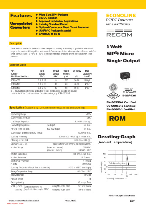
Selection GuidePart Input Output Output Efficiency Max.NumberVoltage Voltage Current Capacitive SIP4 Micro Size Pack.(VDC)(VDC)(mA)(%)Load (1)ROM-xx05S 3.3, 5, 12520070-781000µF ROM-xx12S3.3, 5, 12128378-82470µF ROM-xx15S 3.3, 5, 12156680-84470µFxx = Input Voltage (other input and output voltage combinations available on request)* add Suffix “P” for Continuous Short Circuit Protection, e.g. ROM-0505S/PO u t p u t P o w e r (%)100602040Operating Temperature °C80Specifications (measured at T A = 25°C, nominal input voltage, full load and after warm-up)1 WattSIP4 Micro Single OutputDerating-Graph(Ambient T emperature)●Micro Size SIP4 Package ●3kVDC Isolation●Approved for Medical Applications ●Industry Standard Pinout●Optional Continuous Short Circuit Protected ●UL94V-0 Package Material ●Efficiency to 85%FeaturesUnregulated ConvertersInput Voltage Range ±10%Output Voltage Accuracy ±5%Line Voltage Regulation 1.2%/1% of Vin typ.Load Voltage Regulation 5V Output 15% max.(10% to 100% full load)12V, 15V Output10% max.Output Ripple and Noise (20MHz limited)100mVp-p max.Operating Frequency 50kHz min. / 100kHz typ. / 105kHz max.Efficiency at Full Load 70% min. / 80% typ.Minimum Load = 0%Specifications valid for 10% minimum load only.Isolation Voltage (tested for 1 second)3000VDC (rated for 1 minute)1500VAC / 60Hz Isolation Capacitance 20pF min. / 75pF max.Isolation Resistance 15 G Ωmin.Short Circuit Protection 1 Second P-SuffixContinuousOperating Temperature Range (free air convection)-40°C to +85°C (see Graph)Storage Temperature Range -55°C to +125°CRelative Humidity 95% RHPackage Weight 1gPacking Quantity 42 pcs per TubeMTBF (+25°C)using MIL-HDBK 217F 977 x 103 hours (+85°C)using MIL-HDBK 217F189 x 103 hoursThe ROM Micro Size DC/DC converter has been designed for isolating or converting DC power rails where board height is at a premium. Although it has a micro-size 7.7mm package, it does not compromise on features and offers a high 3kVDC Isolation , a –40°C to +85°C operating temperature range and optional continuous short circuit protection.Description}Detailed Information seeApplication Notes chapter "MTBF"EN-60950-1 Certified UL-60950-1 Certified EN-60601-1 CertifiedREV:1/2011E-17 ECONOLINEDC/DC-Converterwith 3 year WarrantyRefer to Application NotesRoHS2002/95/EC6/6E-224736ROM/E-18REV: 1/2011R O MPackage Style and Pinning (mm)3rd angle projectionRecommended Footprint Details4 PIN SIP Micro Size PackageXX.X ± 0.5 mm XX.XX ± 0.25 mmRO Pin Connections Pin #Single1 –Vin2 +Vin3 –Vout4+VoutTypical CharacteristicsROM SeriesECONOLINEDC/DC-ConverterE f f i c i e n c y %100040%0%100%40Efficiency / Load60%80%20%206080Total Output current (%)Deviation / Load-10.00040%0%100%D e v i a t i o n f r o m N o m in a l (%)60%80%20%-5.000Total Output current (%)0.0005.00010.00015.00020.00025.000E f f i c i e n c y %100040%0%100%40Efficiency / Load 60%80%20%206080Total Output current (%)E f f i c i e n c y %10040%0%100%40Efficiency / Load 60%80%20%206080Total Output current (%)Deviation / Load-10.00040%0%100%D e v i a t i o n f r o m N o m i n a l (%)60%80%20%-5.000Total Output current (%)0.0005.00010.00015.00020.00025.000Deviation / Load-10.00040%0%100%D e v i a t i o n f r o m N o m i n a l (%)60%80%20%-5.000Total Output current (%)0.0005.00010.00015.00020.00025.000ROM-xx05SROM-xx15SROM-xx12SNotes Note 1Maximum capacitive load is defined as the capacitive load that will allow start up in under 1 second without damage to the converter.Certifications CB Test Report Report: US/15348/UL IEC 60950-1:2005 2nd Ed.UL General Safety Report: E224736UL 60950-1 1st Ed.EN General Safety Report: PS080804950C2EN60950-1:2001 + A11:2004EN Medical safetyReport: ETS-0600068AEN 60601-1/分销商库存信息:RECOM-POWERROM-0505S ROM-1212S ROM-0512S ROM-1205S ROM-0515S ROM-1215S ROM-0512S/P ROM-0515S/P ROM-1205S/P ROM-1212S/P ROM-1215S/P ROM-0505S/P。
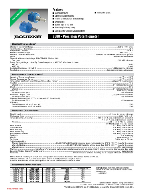
Specifi cations are subject to change without notice.Customers should verify actual device performance in their specifi c applications.*RoHS Directive 2002/95/EC Jan. 27, 2003 including annex and RoHS Recast 2011/65/EU June 8, 2011.Stop Strength..............................................................................................................................................................................45 N-cm (64 oz.-in.) minimum Mechanical Angle ...........................................................................................................................................................................................3600 ° +10 °, -0 °Torque (Starting & Running) ................................................................................................................................0.35 N-cm (0.5 oz.-in.) maximum (unsealed) 1.1 N-cm (1.5 oz.-in.) maximum (sealed) Mounting ..............................................................................................................................................................................55-80 N-cm (5-7 lb.-in.) (plastic) 90-113 N-cm (8-10 in.-lb.) (metal)Shaft Runout......................................................................................................................................................................................0.13 mm (0.005 in.) teral Runout ...................................................................................................................................................................................0.20 mm (0.008 in.) T.I.R.Shaft End Play ...................................................................................................................................................................................0.25 mm (0.010 in.) T.I.R.Shaft Radial Play ...............................................................................................................................................................................0.13 mm (0.005 in.) T.I.R.Pilot Diameter Runout .......................................................................................................................................................................0.08 mm (0.003 in.) T.I.R.Backlash ............................................................................................................................................................................................................1.0 ° maximum Weight ........................................................................................................................................................................................................Approximately 19 G Terminals ................................................................................................................................................................................................Solder lugs or PC pins Soldering ConditionManual Soldering...........................................................96.5Sn/3.0Ag/0.5Cu solid wire or no-clean rosin cored wire; 370 °C (700 °F) max. for 3 seconds Wave Soldering ...................................................................................96.5Sn/3.0Ag/0.5Cu solder with no-clean fl ux; 260 °C (500 °F) max. for 5 seconds Wash processes .......................................................................................................................................................................................Not recommended Marking .....................................Manufacturer’s name and part number, resistance value and tolerance, linearity tolerance, wiring diagram, and date code.Ganging (Multiple Section Potentiometers) ......................................................................................................................................................1 cup maximum Hardware ............................................................................................................One lockwasher and one mounting nut is shipped with each potentiometer.NOTE: For Anti-rotation pin add 91 after confi guration dash number. Example: -2 becomes -291 to add AR pin.1At room ambient: +25 °C nominal and 50 % relative humidity nominal, except as noted. 2Consult manufacturer for complete specifi cation details for resistances below 1k ohms.BOLDFACE LISTINGS ARE IN STOCK AND READILY AVAILABLETHROUGH DISTRIBUTION. FOR OTHER OPTIONS CONSULT FACTORY.ROHS IDENTIFIER: L = COMPLIANTRecommended Part Numbers(Printed Circuit)(Solder Lug)(Solder Lug)Resistance (Ω)Resolution (%)3590P-2-102L 3590S-2-102L 3590S-1-102L 1,000.0293590P-2-202L 3590S-2-202L 3590S-1-202L 2,000.0233590P-2-502L 3590S-2-502L 3590S-1-502L 5,000.0253590P-2-103L 3590S-2-103L 3590S-1-103L 10,000.0203590P-2-203L 3590S-2-203L 3590S-1-203L 20,000.0193590P-2-503L 3590S-2-503L 3590S-1-503L 50,000.0133590P-2-104L3590S-2-104L3590S-1-104L100,000.009*Ro H S C O MP L I A N T/Panel Thickness Dimensions(For Bushing Mount Only)1.60 +.08/-.03(.063 +.003/-.001)DIA.ANTI-ROTATION PINAnti-rotation pin hole is shown at six o'clockposition for reference only. The actual location isdetermined by the customer's application. Referto the front view of the potentiometer to see thelocation of the optional A/R pin.Panel thickness and hole diameters arerecommended for best fit. However, customersmay adjust the dimensions to suit their specificapplication.Product DimensionsSpecifi cations are subject to change without notice.Customers should verify actual device performance in their specifi c applications.REV. 06/12 MOUNTING SURFACE-2, -4, -6, -8 Confi gurations-1, -3, -5, -7 Confi gurationsRecommended PCB LayoutHOLE DIAMETER5.08(.200)5.08(.200)6.99(.275)SchematicTOLERANCES: EXCEPT WHERE NOTED.508 .127DECIMALS: .XX ±(.02),.XXX ±(.005)FRACTIONS: ±1/64MMDIMENSIONS:(IN.)Shaft & Bushing Confi gurations(Bushing - DxL, Shaft - D):(-1) Plastic Bushing (3/8 ” x 5/16 ”)and Shaft (.2480 + .001, - .002)(-2) Metal Bushing (3/8 ” x 5/16 ”)and Shaft (.2497 + .0000, - .0009)(-3) Sealed, Plastic Bushing (3/8 ” x 5/16 ”)and Shaft (.2480 + .001, - .002)(-4) Sealed, Metal Bushing (3/8 ” x 5/16 ”)and Shaft (.2497 + .0000, - .0009)(-5) Metric, Plastic Bushing (9 mm x 7.94 mm)and Shaft (6 mm + 0, - .076 mm)(-6) Metric, Metal Bushing (9 mm x 7.94 mm)and Shaft (6 mm + 0, - .023 mm)(-7) Metric, Sealed, Plastic Bushing (9 mm x7.94 mm) and Shaft (6 mm + 0, - .076 mm)(-8) Metric, Sealed, Metal Bushing (9 mm x7.94 mm) and Shaft (6 mm + 0, - .023 mm)Terminal Styles“P” Terminal Style“S” Terminal Style/分销商库存信息:BOURNS3590S-2-502L3590S-2-102L3590S-2-103L 3590S-2-203L3590S-1-502L3590S-2-104L 3590S-1-203L3590S-2-501L3590S-2-202L 3590S-1-503L3590S-2-503L3590S-1-104L 3590S-291-102L3590S-291-203L3590S-291-502L 3590S-1-201L3590S-1-501L3590S-2-101L 3590S-2-201L3590P-1-102L3590P-1-103L 3590P-1-201L3590P-1-502L3590S-1-102L 3590S-1-103L3590S-2-252L3590P-291-501L 3590P-2-102L3590P-2-201L3590P-2-203L 3590P-2-502L3590S-1-202L3590S-6-102L 3590S-6-201L3590S-6-202L3590S-6-203L 3590S-6-501L3590P-1-104L3590S-6-502L 3590S-4-102L3590S-4-103L3590S-4-202L 3590S-4-203L3590S-4-502L3590S-8-102L 3590S-8-103L3590S-8-202L3590P-2-104L 3590P-4-103L3590P-4-202L3590S-6-503L 3590S-6-104L3590S-4-104L3590P-4-503L 3590P-4-104L3590S-2-5023590S-1-102 3590S-1-1033590S-1-1043590S-1-203 3590S-1-5023590S-1-5033590S-2-102 3590S-2-1033590S-2-1043590S-2-203 3590S-2-5033590S-1-2023590S-2-202 3590S-2-501。
Ra-01S规格书版本V1.1版权©2020免责申明和版权公告本文中的信息,包括供参考的URL地址,如有变更,恕不另行通知。
文档“按现状”提供,不负任何担保责任,包括对适销性、适用于特定用途或非侵权性的任何担保,和任何提案、规格或样品在他处提到的任何担保。
本文档不负任何责任,包括使用本文档内信息产生的侵犯任何专利权行为的责任。
本文档在此未以禁止反言或其他方式授予任何知识产权使用许可,不管是明示许可还是暗示许可。
文中所得测试数据均为安信可实验室测试所得,实际结果可能略有差异。
文中提到的所有商标名称、商标和注册商标均属其各自所有者的财产,特此声明。
最终解释权归深圳市安信可科技有限公司所有。
注意由于产品版本升级或其他原因,本手册内容有可能变更。
深圳市安信可科技有限公司保留在没有任何通知或者提示的情况下对本手册的内容进行修改的权利。
本手册仅作为使用指导,深圳市安信可科技有限公司尽全力在本手册中提供准确的信息,但是深圳市安信可科技有限公司并不确保手册内容完全没有错误,本手册中的所有陈述、信息和建议也不构成任何明示或暗示的担保。
文件制定/修订/废止履历表版本日期制定/修订内容制定核准V1.02020.8.12首版徐V1.12020.8.19更新部分参数徐目录一、产品概述 (5)二、电气参数 (6)三、外观尺寸 (8)四、管脚定义 (10)五、原理图 (11)六、设计指导 (12)七、回流焊曲线图 (14)八、包装信息 (15)九、联系我们 (15)一、产品概述安信可LoRa系列模块(Ra-01S)由安信可科技设计开发。
该模组用于超长距离扩频通信,其射频芯片SX1268主要采用LoRa™远程调制解调器,用于超长距离扩频通信,抗干扰性强,能够最大限度降低电流消耗。
借助SEMTECH的LoRa™专利调制技术,SX1268具有超过-148dBm的高灵敏度,+22dBm的功率输出,传输距离远,可靠性高。
同时,相对传统调制技术,LoRa™调制技术在抗阻塞和选择方面也具有明显优势,解决了传统设计方案无法同时兼顾距离、抗干扰和功耗的问题。