51单片机WR_RD时序
- 格式:doc
- 大小:61.50 KB
- 文档页数:1

计算机工作时,是在统一的时钟脉冲控制下一拍一拍地进行的。
这个脉冲是由单片机控制器中的时序电路发出的。
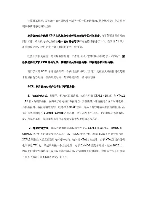
单片机的时序就是CPU在执行指令时所需控制信号的时间顺序,为了保证各部件间的同步工作,单片机内部电路应在唯一的时钟信号下严格地控时序进行工作,在学习51单片机的时序之前,我们先来了解下时序相关的一些概念。
既然计算机是在统一的时钟脉冲控制下工作的,那么,它的时钟脉冲是怎么来的呢?要给我们的计算机CPU提供时序,就需要相关的硬件电路,即振荡器和时钟电路。
我们学习的8051单片机内部有一个高增益反相放大器,这个反相放大器的作用就是用于构成振荡器用的,但要形成时钟,外部还需要加一些附加电路。
8051单片机的时钟产生有以下两种方法:1. 内部时钟方式:利用单片机内部的振荡器,然后在引脚XTAL1(18脚)和XTAL2(19脚)两端接晶振,就构成了稳定的自激振荡器,其发出的脉冲直接送入内部时钟电路,外接晶振时,晶振两端的电容一般选择为30PF左右;这两个电容对频率有微调的作用,晶振的频率范围可在1.2MHz-12MHz之间选择。
为了减少寄生电容,更好地保证振荡器稳定、可靠地工作,振荡器和电容应尽可能安装得与单片机芯片靠近。
2. 外部时钟方式:此方式是利用外部振荡脉冲接入XTAL1或XTAL2。
HMOS和CHMOS单片机外时钟信号接入方式不同,HMOS型单片机(例如8051)外时钟信号由XTAL2端脚注入后直接送至内部时钟电路,输入端XTAL1应接地。
由于XTAL2端的逻辑电平不是TTL的,故建议外接一个上接电阻。
对于CHMOS型的单片机(例如80C51),因内部时钟发生器的信号取自反相器的输入端,故采用外部时钟源时,接线方式为外时钟信号接到XTAL1而XTAL2悬空。
如下图外接时钟信号通过一个二分频的触发器而成为内部时钟信号,要求高、低电平的持续时间都大于20ns,一般为频率低于12MHz的方波。
片内时钟发生器就是上述的二分频触发器,它向芯片提供了一个2节拍的时钟信号。
1、MCS-51单片机的时钟周期与振荡周期之间有什么关系?一个机器周期的时序如何划分?答:时钟周期是单片机最基本的时间单位。
机器周期则是完成某一个规定操作所需的时间。
一个机器周期为6个时钟周期,共12个振荡周期性,依次表示为S1P1、S1P2、……S6P1、S6P2。
2、MCS-51内部四个并行I/O口各有什么异同?作用是什么?答:MCS-51单片机共有四个8位双向并行的I/O端口,每个端口都包括一个锁存器、一个输出驱动器和一个输入缓冲器。
但这四个端口的功能不全相同,P0口既可作一般I/O端口使用,又可作地址/数据总线使用;P1口是一个准双向并行口,作通用并行I/O口使用;P2口除了可作为通用I/O使用外,还可在CPU访问外部存储器时作高八位地址线使用;P3口是一个多功能口除具有准双向I/O功能外,还具有第二功能。
3、简述MCS-51单片机的中断响应过程。
答:CPU在每个机器周期的S5P2期间顺序采样每个中断源,在下一个机器周期S6区间按优先级顺序查询中断标志,如查询到某个中断定标志为1,将在接下来的机器周期S1期间按优先级进行中断处理,中断系统通过硬件自动将相应的中断矢量地址装入 PC,以便进入相应的中断服务程序。
一旦响应中断,CPU首先置位相应的中断“优先级触发器”,然后由硬件执行一条长调用指令,把当前的PC值压入堆栈,以保护断点,再将相应的中断服务的入口地址送入PC,于是CPU接着从中断服务程序的入口处开始执行。
对于有些中断源,CPU在响应中断后会自动清除中断标志。
5、MCS-51单片机内部包括哪些主要逻辑功能部件?答:MCS-51单片机主要由下列部件组成: 1个8位CPU;1个片内振荡器及时钟电路;4KB ROM程序存储器,256BRAM;21个特殊功能寄存器;2个16位定时/计数器;4个8位并行I/O口及1个可编程全双工串行接口;可寻址64KB的外部程序存储器空间;可寻址64KB的外部数据存储器空间;5个中断源、两个优先级中断嵌套中断结构。
P87LPC76x Low Pincount MicrocontrollersProgramming Specifications1999 Feb 18Philips1. PINOUTFigure 1: 20, 16, 8 pins DIP pinoutThe 20 pin SO package outlines SOT163-1 is attached at the end of this document.123RST / V PP / P1.54V SS567891020191817P0.4 / CIN1A / AD1 / PDA16P0.5 / CMPREF / AD2 / PCL 15V DD 1413121112RST / V PP / P1.53V SS45678161514P0.4 / CIN1A / AD1 / PDA 13P0.5 / CMPREF / AD2 / PCL 12V DD 11109RST / V PP / P1.51V SS2348P0.4 / CIN1A / AD1 / PDA 7P0.5 / CMPREF / AD2 / PCL 6V DD5Figure 2: 44 pins PLCC bondout chipTable 1: 44 PLCC pinout (programming related pins are in bold text)PLCC44717392918286401P IN F UNCTION1VSS234 567 8P1.5/RST/VPP 9 10VSS 1112 13141516171819202122P IN F UNCTION44 43 4241403938P0.4/CIN1A/AD1/PDA 37P0.5/CMPREF/AD2/PCL3635 34333231VDD3029282726252423VDD2. PIN DESCRIPTIONSTable 2: Programming pins in different packages3. GETTING INTO THE SERIAL PROGRAMMING MODE1. Disconnect pins PCL and PDA.2. Connect VDD; the part does not support “hot insertion” into the programming socket3. Wait 20 uSec (Min) and raise V PP to 10.75V +/- 0.25V; V PP rise time is 1uSec to 100 uSec.At this point the part is in the programming mode.4. Wait t INIT = 60 uSec (Min) before beginning the serial communication to the part.5. Get out of the programming mode by connecting V PP = 0V; V PP fall time is 1uSec to 100 uSec.6. Disconnect VDD before removing the part from the socket.The programming mode enables the internal RC oscillator.During the programming mode PDA and PCL pins are Schmitt trigger inputs.Figure 3: Getting into the programming modeMNEMONIC44 pins package PIN NO.20 pins packagePIN NO.16 pins packagePIN NO.8 pins packagePIN NO.TYPE NAME AND FUNCTION VSS 10, 1542P Ground: 0V reference.VDD 23, 3115126P Power Supply: 5V +/-.5VPCL 3716137I Serial clock input for EPROM programming communication.PDA 3817148I/O Serial data I/O for EPROM programming communication.VPP8431PV PP = 10.75V +/- 0.25V I PP = 30mA during programming.PDA PCLVDDVPPtVDD = 4.5V to 5.5V; V PP = 10.75V +/- 0.25V I PP = 30mA during programming; T amb = 10°C to +40°C Table 3: Programming mode timings4. PROGRAMMING MODEThe programming commands are sent by the programmer through the PCL and PDA lines. Each programming command is one byte shifted into the part by 8 clocks.The serial interface is identical to the 51’s 8-bit serial UART mode 0; LSB is the first bit in the serial byte.PCL pin is the clock input from the programmer.PDA pin is the data I/O. Data is enabled on the falling edge of PCL, and is clocked on the rising edge of PCL.Data output from the part is disabled after the rising edge of PCL for the last bit in a data byte.Figure 4: Writing programming commands by the programmerTable 4: Programming commandsSYMBOL FIGUREPARAMETERLIMITS UNIT MIN MAX t VDDVPP V DD HIGH to V PP rising edge20us t VPPLH V PP rise time 1100us t VPPHL V PP fall time1100us t INITV PP = 10.75V to the beginning of serial communication60usNAME OPCODE FUNCTIONNOP00H Not usedLOAD_DATA 02H Load address counter with the next data byteRD_DATA 04H Read data byte addressed by the program counterINC_ADDR 06H Increment address counterLD_ADRR_LO 08H Load 8 LOW address bits into programming counter LD_ADRR_HI 0AH Load 8 HIGH address bits into programming counterSTRT_PRGM 0CH Start programming a data byte; always followed by the Stopt programming command STP_PRGM 0EHStop programming a data byte; always follows the Start programming command.PDALSB bitMSB bitPCLNotes:Wait 2 uSec between any two programming commands (except “Start Programming” to “Stop Programming”)Wait 250uSec between “Start Programming” and “Stop Programming” commands.Example of a sequence of programming commandsTable 5: Sequence of programming commandsFigure 5: Reading data by the programmerLD_ADDR_LO Wait 2uSec XX DATA Wait 2uSec LD_ADDR_HI Wait 2uSec XX DATA Wait 2uSec LOAD_DATA Wait 2uSec XX DATA Wait 2uSec READ_DATA Wait 2uSec XX DATA Wait 2uSec INC_ADDR Wait 2uSec LOAD_DATA Wait 2uSec XX DATA Wait 2uSec STRT_PRGM Wait 250uSec STP_PRGMWait 2uSecSYMBOL FIGUREPARAMETERLIMITS UNIT MINMAX t SC 5Serial clock cycle time0.21000us t WAIT 5Wait between two serial bytes2us t WAITP 5Wait after a “Start Programming” command250us t SDSU 4Serial data setup time to the rising edge of the serial clock 40ns t SDH 5Serial data hold time after the rising edge of the serial clock 10ns t SCLDV 5Serial clock LOW to valid data of the first data bit in a byte 40ns t SCHZ5Serial clock HIGH to data Hi-Z at the last data bit in a byte40nsPDALSBMSB PCLTable 6: Programming commands timingAddress Memory Definition0000H to 0FFFH User’s code; program/read by the programmerFC30H Company signature 15H - Read only by programmerFC31H Part’s signature DDH - Read only by the programmerFC60H Derivative’s signature 00H - Read only by the programmerFCE0H to FCFFH32 bytes used as user’s parameters; program/read by the programmerFD00H User Configuration Reg. #1 (UCFG1) program/read by the programmerFD01H User Configuration Reg. #2 (UCFG2) program/read by the programmerTable 7: EPROM MappingThe programmer programs the user’s code at address 0 to FFFH and configuration registers located at address FCE0H to FD01H. These configuration registers configure the chip’s modes of operation.5. USER CONFIGURATION REG. #1 (UCFG1) AT ADDRESS FD00H76543210 Programmed bits WDTE RPD PRHI BO2.5CLKR FOSC2FOSC1FOSC0Erased State FFHTable 8: User Configuration Register #1WDTE: WatchDog Timer Enable;1 = (Erased) WDT enabled0 = (Programmed) WDT disabledRPD: Reset Pin Disable;1(Erased) External Reset pin disabled (The internal power-on reset is enabled)0 (Programmed) External Reset pin enabledPRHI: Port Reset High;1 = Enable ports to high during and after RESET0 = Enable ports to low during and after RESETBO2.5: Brown out at 2.5V;1 = Enable brown out at 2.5V0 = Enable brown out at 3.8VCLKR: CLock Rate select;1 = Enable divide by 1 of clock (6 clocks per machine cycle)0 = Enable divide by 2 of clock (12 clocks per machine cycle)FOSC2 - FOSC0: Oscillator control bits;FOSC2FOSC1FOSC0External clock input at pin X1111Internal RC clock; 6MHz +/- 25%01132KHz to 100KHz external Crystal/Resonator010100KHz to 4 MHz external Crystal/Resonator0014 MHz to 20 MHz external Crystal/Resonator000Table 9: FOSC2-FOSC0 bit function6. USER CONFIGURATION REG. #2 (UCFG2 AT ADDRESS FD01H)76543210 Programmed bits SEC2SEC1Erased State FFHTable 10: User Configuration Register #2SEC2-SEC1: SECurity bits 2 & 1;11 = Security bits unprogrammed; Programming and Verify allowed.10 = Security bit 2 unprogrammed; 1 programmed; Programming disabled, Verify enabled.00 = Both bits programmed; Programming and Verify disabled7. 32 REGISTERS OF USER’S PARAMETERS (FCE0H TO FCFFH)The 32 registers of user’s parameters are programmed as code located at address FCE0H to FCFFH.The content of the 32 parameter registers and the two configuration registers are defined by the HEX file at addresses:FCE0H to FCFFH32 bytes used as user’s parameters; program/read by the programmerFD00H User Configuration Reg. #1 (UCFG1) program/read by the programmerFD01H User Configuration Reg. #2 (UCFG2) program/read by the programmerThe user should be able to display, edit, program and verify the two configuration registers and the user’s 32 bytes located at address FCE0H to FCFFH.Philips SemiconductorsPackage outlinesSO20:plastic small outline package; 20 leads; body width 7.5 mm SOT163-1。
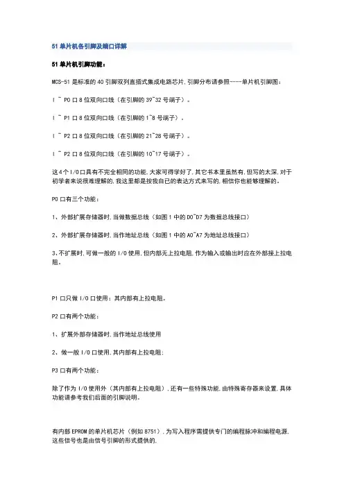
51单片机各引脚及端口详解51单片机引脚功能:MCS-51是标准的40引脚双列直插式集成电路芯片,引脚分布请参照----单片机引脚图:l ~ P0口8位双向口线(在引脚的39~32号端子)。
l ~ P1口8位双向口线(在引脚的1~8号端子)。
l ~ P2口8位双向口线(在引脚的21~28号端子)。
l ~ P2口8位双向口线(在引脚的10~17号端子)。
这4个I/O口具有不完全相同的功能,大家可得学好了,其它书本里虽然有,但写的太深,对于初学者来说很难理解的,我这里都是按我自已的表达方式来写的,相信你也能够理解的。
P0口有三个功能:1、外部扩展存储器时,当做数据总线(如图1中的D0~D7为数据总线接口)2、外部扩展存储器时,当作地址总线(如图1中的A0~A7为地址总线接口)3、不扩展时,可做一般的I/O使用,但内部无上拉电阻,作为输入或输出时应在外部接上拉电阻。
P1口只做I/O口使用:其内部有上拉电阻。
P2口有两个功能:1、扩展外部存储器时,当作地址总线使用2、做一般I/O口使用,其内部有上拉电阻;P3口有两个功能:除了作为I/O使用外(其内部有上拉电阻),还有一些特殊功能,由特殊寄存器来设置,具体功能请参考我们后面的引脚说明。
有内部EPROM的单片机芯片(例如8751),为写入程序需提供专门的编程脉冲和编程电源,这些信号也是由信号引脚的形式提供的,即:编程脉冲:30脚(ALE/PROG)编程电压(25V):31脚(EA/Vpp)接触过工业设备的兄弟可能会看到有些印刷线路板上会有一个电池,这个电池是干什么用的呢这就是单片机的备用电源,当外接电源下降到下限值时,备用电源就会经第二功能的方式由第9脚(即RST/VPD)引入,以保护内部RAM中的信息不会丢失。
在介绍这四个I/O口时提到了一个“上拉电阻”那么上拉电阻又是一个什么东东呢他起什么作用呢都说了是电阻那当然就是一个电阻啦,当作为输入时,上拉电阻将其电位拉高,若输入为低电平则可提供电流源;所以如果P0口如果作为输入时,处在高阻抗状态,只有外接一个上拉电阻才能有效。
单片机时序图MCS51单片机的指令时序接下来我们分别对几个典型的指令时序加以说明。
·单字节单周期指令:单字节单周期指令只进行一次读指令操作,当第二个ALE信号有效时,PC并不加1,那么读出的还是原指令,属于一次无效的读操作。
·双字节单周期指令:这类指令两次的ALE信号都是有效的,只是第一个ALE信号有效时读的是操作码,第二个ALE信号有效时读的是操作数。
·单字节双周期指令:两个机器周期需进行四读指令操作,但只有一次读操作是有效的,后三次的读操作均为无效操作。
单字节双周期指令有一种特殊的情况,象MOVX这类指令,执行这类指令时,先在ROM 中读取指令,然后对外部数据存储器进行读或写操作,头一个机器周期的第一次读指令的操作码为有效,而第二次读指令操作则为无效的。
在第二个指令周期时,则访问外部数据存储器,这时,ALE信号对其操作无影响,即不会再有读指令操作动作。
上页的时序图中,我们只描述了指令的读取状态,而没有画出指令执行时序,因为每条指令都包含了具体的操作数,而操作数类型种类繁多,这里不便列出,有兴趣的读者可参阅有关书籍时序是用定时单位来描述的,MCS-51的时序单位有四个,它们分别是节拍、状态、机器周期和指令周期,接下来我们分别加以说明。
·节拍与状态:我们把振荡脉冲的周期定义为节拍(为方便描述,用P表示),振荡脉冲经过二分频后即得到整个单片机工作系统的时钟信号,把时钟信号的周期定义为状态(用S表示),这样一个状态就有两个节拍,前半周期相应的节拍我们定义为1(P1),后半周期对应的节拍定义为2(P2)。
·机器周期:MCS-51有固定的机器周期,规定一个机器周期有6个状态,分别表示为S1-S6,而一个状态包含两个节拍,那么一个机器周期就有12个节拍,我们可以记着S1P1、S1P2……S6P1、S6P2,一个机器周期共包含12个振荡脉冲,即机器周期就是振荡脉冲的12分频,显然,如果使用6MHz的时钟频率,一个机器周期就是2us,而如使用12MHz的时钟频率,一个机器周期就是1us。
※ 1 ※MCS-51系列单片机的内部结构与时序 内容提要:本文先对MCS-51单片机的外部引脚及内部硬件结构作了简要介绍,再对单片机的工作方式与工作时序作了详细的介绍。
通过本文的学习,可以使读者对MCS-51单片机的硬件结构以及工作原理有较为深刻的了解。
关键字:单片机结构、工作方式、工作时序引言:尽管单片机的型号千差万别,但都无疑或多或少具有部分相同的特征。
了解它们的原理及分析方法对学习和使用其他系列的单片机都有极大的帮助,充分掌握它能使自己设计的单片机系统处于最优的工作方式。
正文:1 MCS-51单片机结构1.1 MCS-51单片机的外部引脚及功能制造工艺为HMOS 的MCS-51都采用40引脚的双列直插式封装(DIP ),其外部引脚配置如图l 所示。
图1 MCS-51单片机外部引脚图CHMOS 制造工艺的80C51/80C31除采用DIP 封装外,还采用方形封装(如PLCC44、QFP44)。
MCS-51单片机的40条引脚按功能来分,可分为三部分。
1. 主电源及时钟引脚包括主电源引脚Vcc 、Vss 、时钟引脚XTAL1、XTAL2。
Vcc (40脚):正常运行、对EPROM 编程和验证时接+5V 电源。
Vss (20脚):接地。
XTAL1(19脚):在单片机内部,它是一个反向放大器的输入端,该放大器构成了片内的振荡器,可提供单片机的时钟控制信号。
该时钟引脚也可接外部晶体振荡器的一个引脚,如果采用外部振荡器时,对HMOS 单片机,此引脚应接地;而对CHMOS 单片机,此引脚作为驱动端。
XTAL2(18脚):在单片机内部,接至上述振荡器的反向输出端。
当采用外部振荡器时,对HMOS 该引脚接收振荡器的信号,即把该信号直接接到内部时钟发生器的输入端;对CHMOS 工艺的,此引脚应悬浮。
2. 控制或与其他电源复用引脚 包括RESET (即RST/VPD )、ALE/PROG 、PSEN 、EA /Vpp ,这类引脚提供控制信号,有些有复用的功能。
MCS-51单片机的指令时序
时序是用定时单位来描述的,MCS-51 的时序单位有四个,它们分别是节拍、状态、机器周期和指令周期,接下来我们分别加以说明。
节拍与状态:我们把振荡脉冲的周期定义为节拍(为方便描述,用P 表示),振荡脉冲经过二分频后即得到整个单片机工作系统的时钟信号,把时钟信号
的周期定义为状态(用S 表示),这样一个状态就有两个节拍,前半周期相应
的节拍我们定义为1(P1),后半周期对应的节拍定义为2(P2)。
机器周期:MCS-51 有固定的机器周期,规定一个机器周期有6 个状态,分别表示为S1-
S6,而一个状态包含两个节拍,那么一个机器周期就有12 个节拍,我们可以
记着S1P1、S1P2……S6P1、S6P2,一个机器周期共包含12 个振荡脉冲,即机器周期就是振荡脉冲的12 分频,显然,如果使用6MHz 的时钟频率,一个机
器周期就是2us,而如使用12MHz 的时钟频率,一个机器周期就是1us。
指令周期:执行一条指令所需要的时间称为指令周期,MCS-51 的指令有单字节、双字节和三字节的,所以它们的指令周期不尽相同,也就是说它们所需的机器
周期不相同,可能包括一到四个不等的机器周期(这些内容,我们将在下面的
章节中加以说明)。
MCS-51 的指令时序:MCS-51 指令系统中,按它们的长度可分为单字节指令、双字节指令和三字节指令。
执行这些指令需要的时间是
不同的,也就是它们所需的机器周期是不同的,有下面几种形式:单字节指令单机器周期单字节指令双机器周期双字节指令单机器周期
双字节指令双机器周期三字节指令双机器周期单字节指令四机器周期(如单
字节的乘除法指令) 下图是MCS-51 系列单片机的指令时序图:。
51单片机各引脚及端口详解51单片机引脚功能:MCS-51是标准的40引脚双列直插式集成电路芯片,引脚分布请参照----单片机引脚图:l ~ P0口8位双向口线(在引脚的39~32号端子)。
l ~ P1口8位双向口线(在引脚的1~8号端子)。
l ~ P2口8位双向口线(在引脚的21~28号端子)。
l ~ P2口8位双向口线(在引脚的10~17号端子)。
这4个I/O口具有不完全相同的功能,大家可得学好了,其它书本里虽然有,但写的太深,对于初学者来说很难理解的,我这里都是按我自已的表达方式来写的,相信你也能够理解的。
P0口有三个功能:1、外部扩展存储器时,当做数据总线(如图1中的D0~D7为数据总线接口)2、外部扩展存储器时,当作地址总线(如图1中的A0~A7为地址总线接口)3、不扩展时,可做一般的I/O使用,但内部无上拉电阻,作为输入或输出时应在外部接上拉电阻。
P1口只做I/O口使用:其内部有上拉电阻。
P2口有两个功能:1、扩展外部存储器时,当作地址总线使用2、做一般I/O口使用,其内部有上拉电阻;P3口有两个功能:除了作为I/O使用外(其内部有上拉电阻),还有一些特殊功能,由特殊寄存器来设置,具体功能请参考我们后面的引脚说明。
有内部EPROM的单片机芯片(例如8751),为写入程序需提供专门的编程脉冲和编程电源,这些信号也是由信号引脚的形式提供的,即:编程脉冲:30脚(ALE/PROG)编程电压(25V):31脚(EA/Vpp)接触过工业设备的兄弟可能会看到有些印刷线路板上会有一个电池,这个电池是干什么用的呢这就是单片机的备用电源,当外接电源下降到下限值时,备用电源就会经第二功能的方式由第9脚(即RST/VPD)引入,以保护内部RAM中的信息不会丢失。
在介绍这四个I/O口时提到了一个“上拉电阻”那么上拉电阻又是一个什么东东呢他起什么作用呢都说了是电阻那当然就是一个电阻啦,当作为输入时,上拉电阻将其电位拉高,若输入为低电平则可提供电流源;所以如果P0口如果作为输入时,处在高阻抗状态,只有外接一个上拉电阻才能有效。
51单片机中WR和RD的使用
例如DAC0832,PDIUSBD12 等芯片,都是并行传输的,且芯片上都的WR 和RD 脚。
在使用这种芯片时可能把WR 和RD 接到51 的普通IO 口上,用普通IO 口来模拟芯片的读写时序来进行对芯片的操作(有些单片机只能用
此方法如AVR 单片机);也可将WR,RD 接到单片机的WR 和RD 上,这时相当于把外部的芯片当外部存储器用。
用这种方法还是很方便的,只要定义好外部芯片的地址。
直接对该地址读写就可以了。
下面拿51 单片机和PDIUSBD12 芯片的读写来说明:
硬件接口:51 的数据口(P0)和PDIUSBD12 的数据口相连;两个
WR,RD,ALE 对应相连;PDIUSBD12 的CS 和P2.7 口相连。
程序如下:
/*-------------------------------------------------------------------*/
# include
#include
#define D12_COMMAND xbyte[0x7f00]
#define D12_DATA xbyte[0x7f01]
void D12WriteCommand(uint8 Command)
{
D12_COMMAND=Command;
}
void D12WriteData(uint8 Data)
{
D12_DATA=Data;。