台湾viking薄膜0603x4贴片排阻TFAN系列选型手册
- 格式:pdf
- 大小:4.47 MB
- 文档页数:5
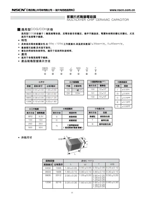
【 南京南山半导体有限公司 — 贴片电容选型资料】MULTILAYER CHIP CERAMIC CAPACITORCOG/COHCOG, ,-55125,030ppm/060ppm/0805CG101J500NT(PF) ( 0402 0.04 0603 0.06 0805 0.08 1206 0.12 ) 0.02 0.03 0.05 0.06 1.00 1.60 2.00 3.20 ( ) 0.50 0.80 1.25 1.60 CG CH COG NPO COH 100 101 102 10 100 1J G C B D5.00% 2.00% 0.25PF 0.10PF 0.50PF10 10 10 1026R3 100 250 5006.3V 10V 25V 50VS C N / / T BWBWTL mm L 0402 0603 0805 1206 1005 1608 2012 3216 1.00 1.60 2.00 3.20 0.05 0.10 0.20 0.30 W 0.50 0.80 1.25 1.60 0.05 0.50 0.10 0.80 0.20 0.80 1.00 1.25 0.20 0.80 1.00 1.25 T WB 0.05 0.25 0.10 0.30 0.20 0.50 0.20 0.20 0.20 0.60 0.20 0.20 0.10 0.10 0.20 0.3015【 南京南山半导体有限公司 — 贴片电容选型资料】0.80 0.20 1.00 0.20 0.50 0.80 0.20 1.00 0.20 0.600.20 0.30【 南京南山半导体有限公司 — 贴片电容选型资料】MULTILAYER CHIP CERAMIC CAPACITORCOG/COH 0402 0603 0805 12066.3V 10V 16V 25V 50V 6.3V 10V 16V 25V 50V 6.3V 10V 16V 25V 50V 6.3V 10V 16V 25V 50V0.5PF 1PF 2PF 3PF 4PF 5PF 6PF 7PF 10PF 22PF 33PF 47PF 68PF 100PF 120PF 150PF 180PF 220PF 330PF 470PF 560PF 680PF 1000PF 2200PF 2700PF 3300PF 4700PF 5600PF 6800PF 10nF 12nF 15nF 22nF 47nF 68nF 100nF17【 南京南山半导体有限公司 — 贴片电容选型资料】04020603080512066.3V 10V 16V 25V 50V 6.3V 10V 16V 25V 50V 6.3V 10V 16V 25V 50V 6.3V 10V 16V 25V 50VCapacitance0.5PF 1PF 2PF 3PF 4PF 5PF 6PF 7PF 10PF 22PF 33PF 47PF 68PF 100PF 120PF 150PF 180PF 220PF 330PF 470PF 560PF 680PF 1000PF 2200PF 2700PF 3300PF 4700PF 5600PF 6800PF 10nF 12nF 15nF 22nF 47nF 68nF 100nF【 南京南山半导体有限公司 — 贴片电容选型资料】MULTILAYER CHIP CERAMIC CAPACITORCOG COHPH~SLCOG PH SH SL TH RH UJCOH1-55125-55851. 2. 3. 2 4. 5. , , , , , 103 4 Cr 5PF 0.56% -4 5PF Cr 50PF 1.5 [(150/Cr)+7] 10 Cr 50PF 0.15% C C 10nF Ri 10nF Ri 5 10 Cr 500s 3 50mA 150+0/-10 8 25 9 75 235 5 2 0.5 25 60 265 10 1 25 : 1 2 100 170 120 200 1 1 2.5mm/ 24 2 5 5 5 2.5mm/ 245 24 -55 125 2 -55 85 60 510:HP4278A 1. 2. 3. (D.F.) :1.0 C : : (HP4284 25 5 0.2V 0.1MHz; 0.1KHZ ) 1000PF,1.0 :SF2511 , 60 60 1 5 :30% 75%5:C<1000PF,1.06I.R.7>3x150+0/-10 5% 0.5PF D.F. 10 I.R. 24 245【 南京南山半导体有限公司 — 贴片电容选型资料】General COGCOHPHSL MLCC reliability test methodStandard Number Item COG COH MLCC for General-use -55 125 PH, RH, SH, TH, UJ, SL MLCC for General-use -55 85 Check by using microscope 10 . Test Method1Operating Temperature RangeAppearance21.Good ceramic body color continuity. 2.The chips have no visual damages and must be very smooth. 3.No exposed inner- electrode, no cracks or holes. 4.The outer electrode should have no cracks, holes, damages or surface oxidation. 5.Outer electrode no prolongation or the prolongation is less than half of that of the termination width.3 4 5Dimensions Capacitance Dissipation Factor (DF)Within the specified dimensions Within the specified tolerance Cr 5PF 0.56% 5PF Cr 50PF 1.5 [(150/Cr)+7] 10-4 Cr 50PF 0.15% C C 10nF Ri 10nF Ri 5 1010 Cr 500sUsing micrometer or vernier calipers Measuring Equipments:HP4278 capacitance meter,HP4284 capacitance, Measuring Conditions: 1.Measuring Temperature:25 5 .Humidity: 30% 75%. 2.Measuring Voltage:1.0 0.2V. 3.Measuring Frequency:C<1000PF 1.0 0.1MHz C 1000PF 1.0 0.1KHz Measuring Equipment:Insulation resistance meter (such as Sf2511 insulation resistance). Measuring Method:Must measure at rated voltage, and measure the IR within 60 5 seconds. Must measure at 3 times rated voltage, dwell time: 60 1 seconds, no short and the changing/discharging current less than 50mA. First, pre-heat: heat treat 60 5 minutes at 150+0/-10 , then set it for 24 2 hours at room temperature. Measure the capacitance at -55 125 or -55 85 , the capacitance change ratio comparing to that of 25 must be within the specified range. Dip the capacitor into ethanol or colophony solution, and then dip it into 235 5 ( or 245 5 leadless eutedtic solder solution ) eutectic solder solution hanving lead for 2 0.5 seconds. Dipping speed: 25 2.5mm/second. First pre-heat: heat treat for 60 5 minutes at 150+0/-10 , then set it for 24 2 hours at room temperature. Then pre-heat the capacitance according to the following chart. Dip the capacitor into 265 5 eutectic solder solution for 10 1 seconds. Then set it for 24 2 hours at room temperature, then measure. Dipping speed: 25 2.5mm/second. Preheat conditions: Stage 1 2 Temperature 100 170 120 200 Time 1minute 1minute6Insulation Resistance7Withstanding Voltage Capacitance Temperature Characteristic>3x rated continuous working voltage Must meet the capacitor character temperature coefficient requirements within the operating temperature range. Tin coverage should be 75% of the outer electrode Appearance Cap. Change ratio DF No defects visible 5%or 0.5PF (whichever is larger)89SolderabilityResistance to Soldering10Same as original spec Same as original specIR46【 南京南山半导体有限公司 — 贴片电容选型资料】MULTILAYER CHIP CERAMIC CAPACITOR1 10N11 10N,10 1 :1.0mm/ 11.5mm 10 D.F. 12 55Hz 210 55Hz 10Hz 6 123 420 mm mmmm13mmmmmmmm150+0/-10 14 24 2 24 260 547【 南京南山半导体有限公司 — 贴片电容选型资料】NumberItems Adhesive Strength of TerminationStandard No removal of the terminations or other defect shall occurTest Method Solder the capacitor to the test jig (glass epoxy resin board) shown in Fig.1 using a eutectic solder.Then apply a 10N force inthe direction shown as the arrowhead.The aoldering shall be done either with an iron or using the reflow method and shall be conducted with care so that an iron or using the refow method and shall be conducted with care so that the soldering is uniform and free of defects such as heat shock,etc. 10N,10 1s Speed:1.0mm/s Glss epoxy resinboard11Fig.1 Vibration Resistance Appearance Capacitance No defects or abnormities Within the specified tolerance range Same as original spec12DFSolder the capacitor to the test jig (glass epoxy resin board). The capacitor should be subjected to a simple harmonic motion having a total amplitude of 1.5mm, the frequency being varied uniformly between the approximate limits of 10 and 55Hz, shall be traversed (from 10 Hz to 55 Hz then 10 Hz again) in approximately 1 minute.This motion shall be applied for a period of 2 hours in each 3 mutually perpendicular directions (total is 6 hours).Same i standarFif.2 Bending Resistance No cracks or other defects shall occur Solder the capacitor to the test jig (glass epoxy resin board) shown in Fig.3 using a eutectic solder. Then apply a 10N force in the direction shown as Fig.4. The soldering shall be done either with an iron or using the reflow method and shall be conducted with care so that the soldering is uniform and free of defects such as mm heat shock, etc.mm13mm mm mm14Temperature CycleAppearance No defects or abnormitiesPre-treatment: Heat-treat the capacitor for 60 5minutes at 150+0/-10 , then set it for 24 2 hours at room temperature. Perform five cycles according to the four heat treatments listed in the following table. Set it for 24 2 hours at room temperature, then measure.48mm【 南京南山半导体有限公司 — 贴片电容选型资料】MULTILAYER CHIP CERAMIC CAPACITOR2.5% 0.25PF, 1 10000M 2 3 4 2 3 30 3 2 3 30 3 2 314D.F. I.R.40 290 95 24 2500+24/-05% 0.5PF, 15 ( ) D.F. I.R. 10000M40 2 500+24/-0 5% 0.5PF, 16 D.F. I.R. 10000M90 95 24 22 50mA 5% 0.5PF, 17 D.F. I.R. 10000M1000 12 24 249【 南京南山半导体有限公司 — 贴片电容选型资料】NumberItem Temperature CycleStandard Cap. Change ratio D.F. I.R. 2.5% or 0.25 PF (whichever is larger) Same as original spec More than 10000M Heat-treatment:Test Method14stage temperature 1 lowest opeating temperature 3 2 normal temperature 3 high operating temperature 2 4 normal temperaturetime min. 30 3 2 3 30 3 2 3Humidity Steady StateAppearance Cap. Change ratio D.F. I.R.No defects or abnormities 5% or 0.5 PF (whichever is larger) Same as original spec More than 10000MSet the capacitor for 500+24/-0 hours at the condition of 40 2 and 90-95% humidity. Then remove and set it for 24 2 hours at room temperature, then measure.15Humidity LoadAppearance Cap. Change ratioNo defects or abnormities 5% or 0.5 PF (whichever is larger) Same as original spec More than 10000MApply rated voltage to the capacitor for 500+24/-0 hours at the condition of 40 2 and 90-95% humidity. Remove and set it for 24 2 hours at room temperature, then measure.16D.F. I.R.Life TestAppearance Cap. Change ratioNo defects or abnormities 5% or 0.5 PF (whichever is larger) Same as original spec More than 10000MApply two times rated voltage to the capacitor for 1000 12 hours at the upper temperature limits, the charging current should be less than 50mA. Remove and set it for 24 2 hours at room temperature, then measure.17D.F. I.R.5057-10%-5%0%5%10%COG 50VX7R 50V Z5U 50V Y5V50V010********-100%-80%-60%-40%-20%0%20%40%[Vdc]COG :1MHZ X7R,Z5U,Y5V:1KHZZ5U 50VY5V 50V X7R 50VC0G 50V0123-20%0%+20%+40%+60%^+80%COG PH RH SH TH UHCOG X7R Y5V,Z5U05010010001000010%0%-10%-20%-30%-40%[Hr]X7R20%0%[Vr ms ]COG :1MHZ X7R,Z5U,Y5V:1KHZMULTILAYER CHIP CERAMIC CAPACITOR58-5%0%5%10%-100%-80%-60%-40%-20%0%20%40%Z5U 50VY5V 50V X7R 50VC0G 50V0123-20%0%+20%+40%+60%^+80%COG X7R Y5V,Z5U05010010001000010%0%-10%-20%-30%-40%0%GENEREL-USE MLCC CHARCCTER PROFILESCapacitance change ratio DC Voltage[Vdc]Measuring condition COG :1MHzX7R,Z5U,Y5V:1KHzCOG and PHRH SH TH UH siriestemperature coefficentDC Capacitance-AC VoltageCharactericsCapacitance change_agingTime[Hr]X7R tempreture characteristicsZ5U [Vr ms ]Capacitance change ratioCapacitance change ratio Capacitance change ratio Capacitance change ratio。
Document Number: 28744For technical questions, contact: *************************** MCS 0402 VG01, MCT 0603 VG01, MCU 0805 VG01 andMCA 1206 VG01 thin film flat chip resistors with establishedreliability are the perfect choice for all high-reliabilityapplications typically found in military, aircraft and spacecraftelectronics. These versions supplement the families ofprofessional and precision thin film flat chip resistorsMCS 0402, MCT 0603, MCU 0805 and MCA 1206.∙Established reliability, failure rate level E6∙Advanced thin film technology ∙Pure Sn termination on Ni barrier layer ∙Single lot date code ∙Material categorization: For definitions of complianceplease see /doc?99912APPLICATIONS∙Military ∙Avionics ∙Space Notes•These resistors do not feature a limited lifetime when operated within the permissible limits. However, resistance value drift increasing over operating time may result in exceeding a limit acceptable to the specific application, thereby establishing a functional lifetime.•The failure rate level E6 (10-6/h, πQ = 0.3), corresponding to MIL Level P, is superior to level E5 (10-5/h, πQ = 1) and thus may be used as areplacement.METRIC SIZE IMPERIAL0402060308051206EN/CECC RR1005M RR1608M RR2012M RR3216M TECHNICAL SPECIFICATIONSDESCRIPTIONMCS 0402 VG01MCT 0603 VG01MCU 0805 VG01MCA 1206 VG01EN/CECC style (size)RR1005M RR1608M RR2012M RR3216MResistance range10 Ωto 1 M Ω; 0Ω 1 Ωto 1 M Ω; 0ΩResistance tolerance± 1 %; ± 0.1 %T emperature coefficient± 50ppm/K; ± 15 ppm/K Rated dissipation, P 700.063W 0.1W 0.125W 0.25W Operating voltage, U max. AC/DC50V 75 V 150V 200V Permissible film temperature, ϑF max.125︒C Operating temperature range- 55 °C to 125 °C Max. resistance change at P 70for resistance range, |∆R /R| max. after:10 Ωto 1 M Ω 1 Ωto 1 M Ω1000h≤ 0.25 %8000h≤ 0.5 %225000h≤ 1.5 %Permissible voltage against ambient(insulation):1 min; U ins75V 100V 200V 300V Continuous75V 75V 75V 75V Assessed failure rate levelE6 = 10-6/h Quality factor, πQ0.3Failure rate: FIT observed < 0.1 x 10⁻⁹/h For technical questions, contact: ***************************Document Number: 28744Notes•The products can be ordered using either the PART NUMBER or the PRODUCT DESCRIPTION.•Products within a packaging unit are single lot date code.TYPE/SIZEVERSION TCR RESISTANCE TOLERANCE PACKAGING MCS 0402MCT 0603MCU 0805MCA 1206H = EN 140401-801,“Version E”;failure rate level E6 C = ± 50 ppm/K E = ± 15 ppm/K Z = Jumper 3 digit value 1 digit multiplier MULTIPLIER8 = *10-29 = *10-10 = *1001 = *1012 = *1023 = *1034 = *1040000 = Jumper F = ± 1 %B = ± 0.1 %Z = JumperE1E0P1P5Product Description: MCT 0603-50 1% VG01 P5 287KProduct Description: MCT 0603 VG01 P5 0R0MCT 0603-50 1 %VG01P5287K MCT 0603--VG01P50R0TYPE/SIZETCR T OLERANCE VERSION PACKAGING RESISTANCE MCS 0402MCT 0603MCU 0805MCA 1206± 50 ppm/K ± 15 ppm/K ± 1 %± 0.1 %VG01 = EN 140401-801,“Version E”;failure rate level E6E1E0P1P549R9 = 49.9 Ω287K = 287 k Ω0R0 = JumperMC T 0603H Z 0000Z P 50006032873500Document Number: 28744For technical questions, contact: *************************** Note•The ordering information according to EN 140401-801:2007 shown above succeeds and replaces the ordering information according to earlier versions of the detail specification EN 140401-801 or its predecessor CECC 40401-801, for example:CECC 40401-801 EZ RR1608M C 287K F E6CECC 40401-801 S RR1608M C 287K F E6with EZ; S Assessment level, where EZ is successor to and superior replacement for SRR1608M Style, with suffix M for “metric”C Temperature coefficient, according to the detail specificationC = ± 50 ppm/K; E = ± 15 ppm/K Note•According to EN 140401-801, resistance values are to be selected from the E96 series for ±1% tolerance and from the E192 series for ±0.1 % tolerance.EN140401-801EZRR1608M-0R00-E6The elements used in the component number have the following meaning:EN140401-801EZRR1608MR287KF E6EN detail specification number Assessment level for the zero-defect approach Style (size)T emperature coefficient, according to EN 60062R = ± 50 ppm/K; P = ± 15 ppm/K Resistance, according to EN 60062, 4 characters T olerance on rated resistance, according to EN 60062F = ± 1 %; B = ± 0.1 %Failure rate level according to EN 60115-1, annex ZRTEMPERATURE COEFFICIENT AND RESISTANCE RANGEDESCRIPTIONRESISTANCE TCRTOLERANCE MCS 0402 VG01MCT 0603 VG01MCU 0805 VG01MCA 1206 VG01± 50 ppm/K± 1 %10 Ωto 1 M Ω 1 Ωto 1 M Ω1Ωto 1 M Ω1Ωto 1 M Ω± 15 ppm/K± 0.1 %100Ωto 33.2 k Ω100Ωto 47.5 k Ω100Ωto 100k Ω43.2Ωto 332k ΩJumper ≤ 20m Ω; I max. = 0.63 A ≤ 20m Ω; I max. = 1 A ≤ 20m Ω; I max. = 1.5 A≤ 20m Ω; I max. = 2 A PACKAGINGTYPECODE QUANTITY CARRIER TAPE WIDTH PITCH REEL DIAMETER MCS 0402 VG01E11000Paper tape acc. IEC 60286-3T ype I 8 mm 2 mm 180 mm/7"E010 000MCT 0603 VG01P110008 mm 4 mm P55000MCU 0805 VG01P11000P55000MCA 1206 VG01P11000P55000 For technical questions, contact: ***************************Document Number: 28744Note•Resistors MCA 1206 VG01 and MCU 0805 VG01 are marked using to the four-character code system of IEC 60062, 4.2.3.Resistors MCT 0603 VG01 and MCS 0402 VG01 do not show any marking on their light blue protective coating.Note•The given solder pad dimensions reflect the considerations for board design and assembly as outlined e.g. in standards IEC 61188-5-x, or in publication IPC 7351. They do not guarantee any supposed thermal properties, however, they will be found adequate for most general applications.DIMENSIONS AND MASSTYPEH (mm)L (mm)W (mm)W T (mm)T b (mm)T t (mm)MASS (mg)MCS 0402 VG010.32 ± 0.05 1.0 ± 0.050.5 ± 0.05> 75 % of W 0.2 ± 0.10.2 + 0.1/- 0.150.6MCT 0603 VG010.45 + 0.1/- 0.05 1.55 ± 0.050.85 ± 0.10.3 + 0.15/- 0.21.9MCU 0805 VG010.45 + 0.1/- 0.052.0 ± 0.11.25 ± 0.150.4 + 0.1/- 0.2 4.6MCA 1206 VG010.55 ± 0.1 3.2 + 0.1/- 0.2 1.6 ± 0.150.5 ± 0.259.2RECOMMENDED SOLDER PAD DIMENSIONSTYPE WAVE SOLDERINGREFLOW SOLDERING G(mm)Y (mm)X (mm)Z (mm)G (mm)Y (mm)X (mm)Z(mm)MCS 0402 VG01----0.350.550.55 1.45MCT 0603 VG010.551.10 1.102.750.650.700.95 2.05MCU 0805 VG010.801.25 1.50 3.300.900.90 1.402.70MCA 1206 VG011.40 1.50 1.90 4.40 1.50 1.15 1.753.80grade ceramic (Al2O3) substrate and conditioned to achieve the desired temperature coefficient. Specially designed inner contacts are deposited on both sides. A special laser is used to achieve the target value by smoothly cutting a meander groove in the resistive layer without damaging the ceramics. For the high ohmic range, optimized cermet products provide comparable properties. The resistor elements are covered by a protective coating designed for electrical, mechanical and climatic protection. The terminations receive a final pure tin on nickel plating.The result of the determined production is verified by an extensive testing procedure performed on 100 % of the individual resistors. This includes pulse load screening for the elimination of products with a potential risk of early life failures according to EN 140401-801, 2.1.2.2 (feasible for R≥ 10 Ω). Only accepted products are laid directly into the paper tape in accordance with EN 60286-3 (3), Type I.Products within a packaging unit are from the same production lot and carry the same date code.ASSEMBLYThe resistors are suitable for processing on automatic SMD assembly systems. They are suitable for automatic soldering using wave, reflow or vapour phase as shown in IEC61760-1 (3). Solderability is specified for 2 years after production or requalification. The permitted storage time is 20 years.The resistors are RoHS compliant; the pure tin plating provides compatibility with lead (Pb)-free soldering processes. The immunity of the plating against tin whisker growth has been proven under extensive testing.The encapsulation is resistant to all cleaning solvents commonly used in the electronics industry, including alcohols, esters and aqueous solutions. The suitability of conformal coatings, if applied, shall be qualified by appropriate means to ensure the long-term stability of the whole system.∙2000/53/EC End of Vehicle life Directive (ELV) and Annex II (ELV II)∙2011/65/EU Restriction of the use of Hazardous Substances directive (RoHS)∙2002/96/EC Waste Electrical and Electronic Equipment Directive (WEEE)APPROVALSThe resistors are approved within the IECQ-CECC Quality Assessment System for Electronic Components to the detail specification EN140401-801 which refers to EN60115-1, EN140400 and the variety of environmental test procedures of the IEC 60068 (3)series.Conformity is attested by the use of the CECC logo () as the mark of conformity on the package label.Vishay BEYS C HLAG has achieved “Approval of Manufacturer” in accordance with IEC QC001002-3, clause 2. The release certificate for “Technology Approval Schedule” in accordance with CECC240001 based on IEC QC001002-3, clause 6 is granted for the Vishay BEYSCHLAG manufacturing process.The Vishay BEYSC HLAG production facility is registered with the CAGE code D9539.RELATED PRODUCTSA wider range of TCR, tolerance and resistance values, plus the option of values from a different E series is available with products approved to EN 140401-801, Version A, without established reliability, nominal failure rate level E0 (quality factor πQ = 3). See the datasheets:∙“Professional Flat Chip Resistors”(/doc?28705)∙“Precision Flat Chip Resistors”(/doc?28700)Notes(1)Global Automotive Declarable Substance List, see .(2)CEFIC (European Chemical Industry Council), EECA (European Electronic Component Manufacturers Association), EICTA (European tradeorganisation representing the information and communications technology and consumer electronics), see /index.php?id=1053&id_article=340.(3)The quoted IEC standards are also released as EN standards with the same number and identical contents.Document Number: 28744For technical questions, contact: *************************** For technical questions, contact: ***************************Document Number: 28744Document Number: 28744For technical questions, contact: *************************** •“Precision Flat Chip Resistors”, document no. 28700EN 140400, sectional specificationEN 140401-801, detail specificationFor further information on the tests and requirements ofthese products please refer to the specifications mentionedabove, and to the following datasheets:•“Professional Flat Chip Resistors”(/doc?28705)•“Precision Flat Chip Resistors”(/doc?28700)HISTORICAL 12NC INFORMATION∙The resistors had a 12-digit code starting with 2312∙The subsequent 4 digits indicated the resistor type,specification and packaging; see the 12NC table∙The remaining 4digits indicate the resistance value:-The first 3digits indicated the resistance value-The last digit indicated the resistance decade inaccordance with the resistance decade table RESISTANCE DECADE Historical 12NC ExampleThe 12NC of a MC T 0603 VG01 resistor, value 287K andTCR 50 with ± 1 % tolerance, supplied in cardboard tape of5000units per reel was: 2312 215 02874.RESISTANCE DECADE LAST DIGIT 1Ω to 9.99Ω810Ω to 99.9Ω9100Ω to 999Ω11 k Ωto 9.99k Ω210k Ω to 99.9k Ω3100k Ω to 999k Ω41M Ω5HISTORICAL 12NC - Resistor type and packagingDESCRIPTION2312........CARDBOARD TAPE ON REEL TYPE TCRTOL.E1 1000 PIECES E0 10 000 PIECES MCS 0402 VG01± 50 ppm/K± 1 %260 0....275 0....± 15 ppm/K± 0.1 %262 0....277 0....Jumper262 90001277 90001TYPE TCRTOL.P11000 PIECES P5 5000 PIECES PW 20 000 PIECES MCT 0603 VG01± 50 ppm/K± 1 %200 0....215 0....205 0....± 15 ppm/K± 0.1 %202 0....217 0....-Jumper202 90001217 90001207 90001MCU 0805 VG01± 50 ppm/K±1 %240 0....255 0....245 0....± 15 ppm/K± 0.1 %242 0....257 0....-Jumper242 90001257 90001247 90001MCA 1206 VG01± 50 ppm/K± 1 %No 12NC assigned to MCA 1206 VG01± 15 ppm/K± 0.1 %Jumper“Vishay”), disclaim any and all liability for any errors, inaccuracies or incompleteness contained in any datasheet or in any other disclosure relating to any product.Vishay makes no warranty, representation or guarantee regarding the suitability of the products for any particular purpose or the continuing production of any product. To the maximum extent permitted by applicable law, Vishay disclaims (i) any and all liability arising out of the application or use of any product, (ii) any and all liability, including without limitation special, consequential or incidental damages, and (iii) any and all implied warranties, including warranties of fitness for particular purpose, non-infringement and merchantability.Statements regarding the suitability of products for certain types of applications are based on Vishay’s knowledge of typical requirements that are often placed on Vishay products in generic applications. Such statements are not binding statements about the suitability of products for a particular application. It is the customer’s responsibility to validate that a particular product with the properties described in the product specification is suitable for use in a particular application. Parameters provided in datasheets and/or specifications may vary in different applications and performance may vary over time. All operating parameters, including typical parameters, must be validated for each customer application by the customer’s technical experts. Product specifications do not expand or otherwise modify Vishay’s terms and conditions of purchase, including but not limited to the warranty expressed therein.Except as expressly indicated in writing, Vishay products are not designed for use in medical, life-saving, or life-sustaining applications or for any other application in which the failure of the Vishay product could result in personal injury or death. Customers using or selling Vishay products not expressly indicated for use in such applications do so at their own risk. Please contact authorized Vishay personnel to obtain written terms and conditions regarding products designed for such applications. No license, express or implied, by estoppel or otherwise, to any intellectual property rights is granted by this document or by any conduct of Vishay. Product names and markings noted herein may be trademarks of their respective owners.Material Category PolicyVishay Intertechnology, Inc. hereby certifies that all its products that are identified as RoHS-Compliant fulfill the definitions and restrictions defined under Directive 2011/65/EU of The European Parliament and of the Council of June 8, 2011 on the restriction of the use of certain hazardous substances in electrical and electronic equipment (EEE) - recast, unless otherwise specified as non-compliant.Please note that some Vishay documentation may still make reference to RoHS Directive 2002/95/EC. We confirm that all the products identified as being compliant to Directive 2002/95/EC conform to Directive 2011/65/EU.Vishay Intertechnology, Inc. hereby certifies that all its products that are identified as Halogen-Free follow Halogen-Free requirements as per JEDEC JS709A standards. Please note that some Vishay documentation may still make reference to the IEC 61249-2-21 definition. We confirm that all the products identified as being compliant to IEC 61249-2-21 conform to JEDEC JS709A standards.Revision: 02-Oct-121Document Number: 91000。
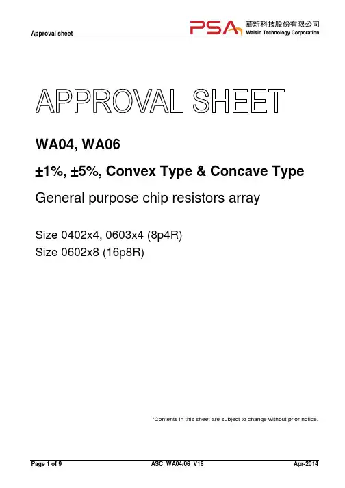
Approval sheetWA04, WA06 ±1%, ±5%, Convex Type & Concave Type General purpose chip resistors arraySize 0402x4, 0603x4 (8p4R) Size 0602x8 (16p8R)Page 1 of 9*Contents in this sheet are subject to change without prior notice.ASC_WA04/06_V16Apr-2014Approval sheetFEATURE1. Small size and light weight 2. Reduced size of final equipment 3. Lower surface mounted assembly costs 4. Higher component and equipment reliability 5. RoHS compliant and lead free products.APPLICATION• Consumer electrical equipment • EDP, Computer application • TelecomDESCRIPTIONThe resistors array is constructed in a high grade ceramic body (aluminum oxide). Internal metal electrodes are added at each end and connected by a resistive paste that is applied to the top surface of the substrate. The composition of the paste is adjusted to give the approximate resistance required and the value is trimmed to within tolerance by laser cutting of this resistive layer. The resistive layer is covered with a protective coat. Finally, the two external end terminations are added. For ease of soldering the outer layer of these end terminations is Tin (lead free) alloy.Fig 1. Construction of a Chip-R array (convex Type)Fig 2. Construction of a Chip-R array (concave Type)Page 2 of 9ASC_WA04/06_V16Apr-2014Approval sheetQUICK REFERENCE DATAItemSeries No. Size Resistance ToleranceResistance RangeTCR (ppm/°C) 10Ω ≤ R ≤ 1MΩ R<10Ω, R>1MΩ Max. dissipation at Tamb=70°C Max. Operation Voltage (DC or RMS) Max. overload voltage Climatic categoryWA04X(Convex) 0402x4 (1005x4)±1%±5%10Ω ~ 1MΩ1Ω ~ 1MΩ Jumper≤ ± 200 -≤ ± 200 ≤ ± 2501/16 W50V100V 55/155/56Note :General Specification WA06X(Convex) 0603x4 (1608x4)WA06W(Convex) 0602x8 (1605x8)WA06T(Concave) 0603x4 (1608x4)±1%±5%±1%±5%±1%±5%10Ω ~ 1MΩ 1Ω ~ 10MΩ 10Ω ~ 100KΩ, 10Ω ~ 100KΩ 10Ω ~ 1MΩ, 10Ω ~ 1MΩ,Jumper,Jumper,Jumper≤ ±100 -≤ ±200 -300~+5001/10 W≤ ±200 -≤ ± 200 -1/16 W≤ ± 200 -≤ ± 200 -1/10 W50V50V50V100V100V 55/155/56100V 55/155/561. Climatic category refer to IEC 600682. This is the maximum voltage that may be continuously supplied to the resistor element, see “IEC publication 60115-8”3. Max. Operation Voltage : So called RCWV (Rated Continuous Working Voltage) is determined byRCWV = Rated Power × Resistance Value or Max. RCWV listed above, whichever is lower.DIMENSIONS (unit : mm)WA04XWA06XL2.00 ± 0.103.20 ± 0.10W1.00 ± 0.101.60 ± 0.10T0.45 ± 0.100.50 ± 0.10P0.50 ± 0.050.80 ± 0.10A0.40 ± 0.100.60 ± 0.10B0.20 ± 0.100.30 ± 0.10C0.30 ± 0.050.40 ± 0.10G0.25 ± 0.100.30 ± 0.20Page 3 of 9ASC_WA04/06_V16Apr-2014Approval sheetWA06WL4.00 ± 0.20W1.60 ± 0.15T0.45 ± 0.10B0.30 ± 0.20G0.30 ± 0.20D0.20 ± 0.10P0.50 ± 0.20H10.40 ± 0.20H20.30 ± 0.10WA06TL3.20+0.20/-0.10W1.60+0.20/-0.10T0.60 ± 0.10P0.80 ± 0.10A0.60 ± 0.15B0.35 ± 0.15C0.50 ± 0.15G0.50 ± 0.15Page 4 of 9ASC_WA04/06_V16Apr-2014Approval sheetMARKING3-digits marking for E24 series 1% ,5% productsEach resistor is marked with a three digits code on the protective coating to designate the nominal resistance value. For values up to 9.1 the R is used as a decimal point. For values of 10.0 or greater the first 2 digits apply to the resistance value and third indicate the number of zeros to follow.ExampleRESISTANCE4.7Ω10Ω100Ω6800Ω47000Ω3-digits marking4R7100101682473FUNCTIONAL DESCRIPTIONProduct characterizationStandard values of nominal resistance are taken from the E24 series for resistors with a tolerance of ±5%, The values of the E24 series are in accordance with “IEC publication 60063” Standard values of nominal resistance are taken from the E24/E96 series for resistors with a tolerance of ±1%, The values of the E24/E96 series are in accordance with “IEC publication 60063”DeratingThe power that the resistor can dissipate depends on the operating temperature; see Fig.3.Figure 3 Maximum dissipation in percentage of rated power as a function of the ambient temperatureCONSTRUCTIONPage 5 of 9R1=R2=R3=R4 ASC_WA04/06_V16Apr-2014Approval sheetMOUNTINGDue to their rectangular shapes and small tolerances, Surface Mountable Resistors are suitable for handling by automatic placement systems. Chip placement can be on ceramic substrates and printed-circuit boards (PCBs). Electrical connection to the circuit is by individual soldering condition. The end terminations guarantee a reliable contact.SOLDERING CONDITIONThe robust construction of chip resistors allows them to be completely immersed in a solder bath of 260°C for 10 seconds. Therefore, it is possible to mount Surface Mount Resistors on one side of a PCB and other discrete components on the reverse (mixed PCBs). Surface Mount Resistors are tested for solderability at 235°C during 2 seconds. The test condition for no leaching is 260°C for 30 seconds. Typical examples of soldering processes that provide reliable joints without any damage are given in Fig 4.Fig 4. Infrared soldering profile for Chip Resistors arrayPage 6 of 9ASC_WA04/06_V16Apr-2014Approval sheetTEST AND REQUIREMENTS(JIS C 5201-1 : 1998)Essentially all tests are carried out according to the schedule of IEC publication 115-8, category LCT/UCT/56(rated temperature range : Lower Category Temperature, Upper Category Temperature; damp heat, long term, 56 days). The testing also meets the requirements specified by EIA, EIAJ and JIS.The tests are carried out in accordance with IEC publication 68, "Recommended basic climatic and mechanical robustness testing procedure for electronic components" and under standard atmospheric conditions according to IEC 60068-1, subclause 5.3. Unless otherwise specified, the following value supplied :Temperature: 15°C to 35°C. Relative humidity: 45% to 75%. Air pressure: 86kPa to 106 kPa (860 mbar to 1060 mbar).All soldering tests are performed with midly activated flux.TESTDC resistance Clause 4.5Temperature Coefficient of Resistance (T.C.R) Clause 4.8Short time overload (S.T.O.L) Clause 4.13 Resistance to soldering heat(R.S.H) Clause 4.18 Solderability Clause 4.17 Temperature cycling Clause 4.19Load life (endurance) Clause 4.25Load life in Humidity Clause 4.24Adhesion Clause 4.32 Insulation Resistance Clause 4.6 Dielectric Withstand Voltage Clause 4.7PROCEDUREREQUIREMENTResistorJumperDC resistance values measured at the test voltages specified below :Within the specified< 50mΩ<10Ω@0.1V,<100Ω@0.3V,<1KΩ@1.0V,<10KΩ@3V, <100KΩ@10V, tolerance <1MΩ@25V, <10MΩ@30VNatural resistance change per change in degree centigrade.( ) R2 − R1 ×106 (ppm/°C)R1 t2 − t1t1 : 20°C+5°C-1°CRefer toN/a“QUICK REFERENCE DATA”R1 : Resistance at reference temperature R2 : Resistance at test temperature Permanent resistance change after a 5second application of a ∆R/R max. ±(2%+0.10Ω)< 50mΩvoltage 2.5 times RCWV or the maximum overload voltage specifiedin the above list, whichever is less.Un-mounted chips completely immersed for 10±1second in a SAC ΔR/R max. ±(1%+0.05Ω)solder bath at 260℃±5ºCno visible damage< 50mΩUn-mounted chips completely immersed for 2±0.5 second in a SAC good tinning (>95% covered)solder bath at 235℃±5℃no visible damage30 minutes at -55°C±3°C, 2~3 minutes at 20°C+5°C-1°C, 30 ΔR/R max. ±(1%+0.05Ω)minutes at +155°C±3°C, 2~3 minutes at 20°C+5°C-1°C, total 5 no visible damagecontinuous cycles1000 +48/-0 hours, loaded with RCWV or Vmax in chamber ΔR/R max.±(3%+0.10Ω)controller 70±2ºC, 1.5 hours on and 0.5 hours offFor 10Ω≤R<1MΩ ;ΔR/R max.±(5%+0.10Ω)< 50mΩ < 50mΩ1000 +48/-0 hours, loaded with RCWV or Vmax in humidity chambercontroller at 40°C±2°C and 90~95% relative humidity, 1.5hours on and 0.5 hours offFor R<10Ω, R≥1MΩ ΔR/R max.±(3%+0.10Ω)For 10Ω≤R<1MΩ ; ΔR/R max.±(5%+0.10Ω)< 50mΩPressurizing force: 5N, Test time: 10±1sec. Apply the maximum overload voltage (DC) for 1minuteFor R<10Ω, R≥1MΩ No remarkable damage or removal of the terminations. R≧10GΩApply the maximum overload voltage (AC) for 1 minuteNo breakdown or flashoverPage 7 of 9ASC_WA04/06_V16Apr-2014Approval sheetTEST CONDITION FOR JUMPER (0 Ω)ItemWA04YWA04XPower Rating At 70°C1/16W1/16WResistanceMAX.50mΩMAX.50mΩRated Current1A1APeak Current1.5A1.5AOperating Temperature-55~155°C-55~155°CWA06X 1/10W MAX.50mΩ1A 3A -55~155°CWA06W 1/16W MAX.50mΩ2A 3A -55~155°CWA06T 1/10W MAX.50mΩ1A 3A -55~155°CCATALOGUE NUMBERSThe resistors have a catalogue number starting with .WAXXXXXXXLSize codeType codeResistance codeTolerance Packaging code Termination code06: 0603 (1608) 04:0402(1005)X : x 4, Convex W :x 8, Convex T : x 4, Concave5% E24 : 2 significant digits followed by no. of zeros and a blank4.7Ω=4R7_F: ±1% J : ±5% P : Jumper10Ω=100_T : 7” Reel taping B : Bulk G : 13” Reel tapingL = Sn base (lead free)220Ω Jumper=221_ =000_(“_” means a blank)1%, E24+E96: 3 significant digits followed by no. of zeros100Ω=100037.4KΩ =3742WA06X, WA06T1. Reeled tape packaging : 8mm width paper taping 5000pcs per 7” reel; 20,000pcs per 13” reel.2. Bulk packaging: 5000pcs per polybagWA06W1. Reeled tape packaging : 12mm width paper taping 5000pcs per 7” reel.2. Bulk packaging: 5000pcs per polybagWA04X, . Reeled tape packaging : 8mm width paper taping 10,000pcs per 7” reel; 40,000pcs per 13” reel.Page 8 of 9ASC_WA04/06_V16Apr-2014Approval sheetPACKAGINGPaper Tape specifications (unit :mm)Symbol WA06X,WA06TWA04XA 3.60±0.20 2.20±0.20WA06W4.20+0.2 − 0.0Symbol WA06X,WA06TWA04XWA06WP1 4.00±0.10 2.00±0.05 4.00±0.10Reel dimensionsB 2.00±0.20 1.20±0.20W 8.00±0.30F 3.50±0.201.80+0.12 − 0.012.00±0.105.50±0.05P0 4.00±0.10ΦDΦ1.50+0.1 −0.0∅D1.55±0.05T Max. 1.0 Max. 0.60.80±0.05E 1.75±0.10 1.75±0.10Symbol WA06X,WA04X,WA06TWA06WA Φ178.0±2.0 Φ178.0±2.0B Φ60.0±1.0 Φ60.0±1.0C 13.0±0.2 13.0±0.2D 9.0±0.5 12.4±1.0Page 9 of 9ASC_WA04/06_V16Apr-2014。
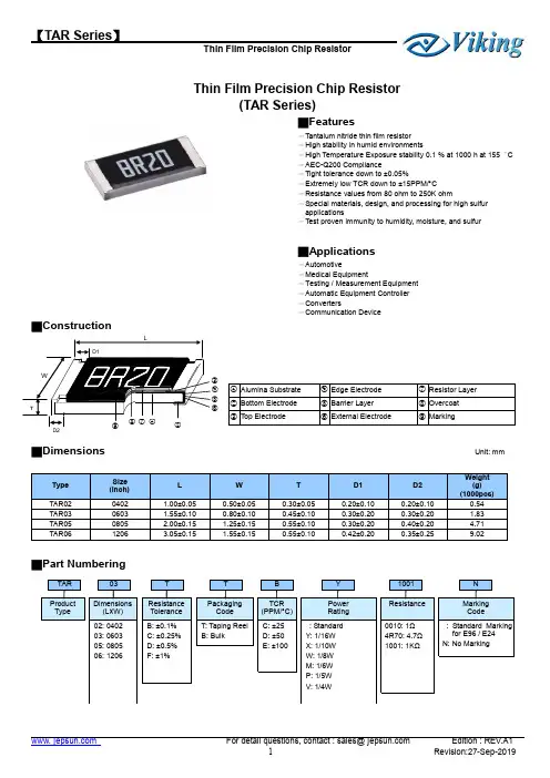
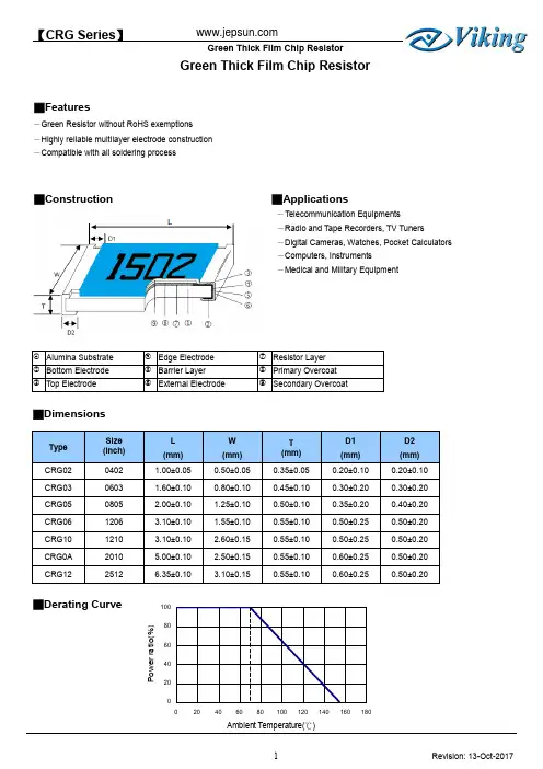
Green Thick Film Chip Resistor■Features-Green Resistor without RoHS exemptions -Highly reliable multilayer electrode construction -Compatible with all soldering process■Construction ■Applications-Telecommunication Equipments -Radio and Tape Recorders, TV Tuners -Digital Cameras, Watches, Pocket Calculators -Computers, Instruments -Medical and Military Equipment■Dimensions■Part NumberingPart Number :CRG03FL7---10R Part Number :CRG03JL7----0R■Standard Electrical SpecificationsOperating Voltage=√(P*R) or Max. operating voltage listed above, whichever is lower. Overload Voltage=2.5*√(P*R) or Max. overload voltage listed above, whichever is lower. ■ Viking is capable of manufacturing the optional spec based o n customer’s requirement.■Soldering ConditionIR Reflow Soldering Wave Soldering (Flow Soldering)(1) Time of IR reflow soldering at maximum temperature point 260︒C :10s (2) Time of wave soldering at maximum temperature point 260︒C :10s (3) Time of soldering iron at maximum temperature point 410︒C :5s■Recommend Land PatternRCWV(Rated Continuous Working Voltage)=√(P*R) or Max. Operating Voltage whichever is lower.■Storage Temperature: 15~28°C; Humidity < 80%RH▓Packaging ArrayReel Specifications & Packaging QuantityPaper Tape SpecificationsEmbossed Plastic Tape Specifications■MarkingNo Marking for 0402 Jumper for all: Letter “0”1% for 0805/1206/1210/2010/2512: 4 digits markingExample:5% for 0603/0805/1206/1210/2010/2512: 3 digits marking in E24Example: 101=100Ω 102=1K Ω (1stand 2ndare E24 code and 3rdcode is multiplier)1% for 0603(E24): 3 digits marking in E24, When the E24 and E96 are the same resistance, this marking in E96 Example: 01A= 100Ω 05C=11K Ω 123=12K Ω 273=27K ΩTop TapeBottom TapeψD 11.5+0.25,-01% for 0603: 3 digits marking in E963 digits marking for Example: 14C=13K7Ω 13C=13K3Ω68B=4K99Ω 68X=49.9Ω14C。
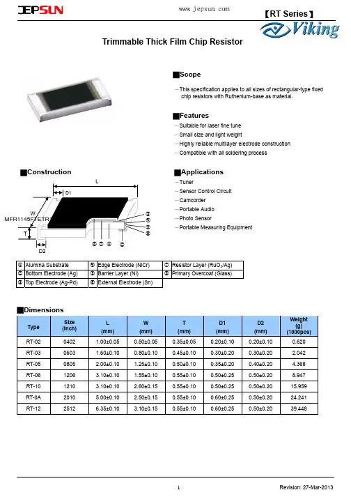
Trimmable Thick Film Chip Resistor■Scope-This specification applies to all sizes of rectangular-type fixed chip resistors with Ruthenium-base as material.■Features-Suitable for laser fine tune -Small size and light weight-Highly reliable multilayer electrode construction -Compatible with all soldering process■Construction ■Applications-Tuner-Sensor Control Circuit -Camcorder -Portable Audio -Photo Sensor-Portable Measuring Equipment■DimensionsType Size (Inch) L (mm)W (mm)T (mm)D1 (mm)D2 (mm)Weight (g)(1000pcs)RT-02 04021.00±0.05 0.50±0.05 0.35±0.05 0.20±0.10 0.20±0.10 0.620 RT-03 0603 1.60±0.10 0.80±0.10 0.45±0.10 0.30±0.20 0.30±0.202.042 RT-05 0805 2.00±0.10 1.25±0.10 0.50±0.10 0.35±0.20 0.40±0.20 4.368 RT-06 12063.10±0.10 1.55±0.10 0.55±0.10 0.50±0.25 0.50±0.20 8.947 RT-10 1210 3.10±0.10 2.60±0.15 0.55±0.10 0.50±0.25 0.50±0.20 15.959 RT-0A 2010 5.00±0.10 2.50±0.15 0.55±0.10 0.60±0.25 0.50±0.20 24.241 RT-1225126.35±0.10 3.10±0.15 0.55±0.10 0.60±0.25 0.50±0.20 39.4481 Alumina Substrate 4 Edge Electrode (NiCr) 7Resistor Layer (RuO 2/Ag)2 Bottom Electrode (Ag) 5 Barrier Layer (Ni)8Primary Overcoat (Glass)3 Top Electrode (Ag-Pd) 6 External Electrode (Sn)D112345678【】深圳捷比信--高品质精密元件供应商www.jepsun.comRT Series■Part Numbering■Recommend Land Pattern■Derating Curve■Soldering ConditionIR Reflow Soldering Wave Soldering (Flow Soldering)(1) Time of IR reflow soldering at maximum temperature point 260°C:10s(2) Time of wave soldering at maximum temperature point 260°C:10s(3) Time of soldering iron at maximum temperature point 410°C:5sTypeA(mm)B(mm)C(mm)RT-02 0.50 0.45 0.60RT-03 0.90 0.60 0.90RT-05 1.20 0.70 1.30RT-062.00 0.90 1.60RT-10 2.00 0.90 2.80RT-0A 3.80 0.90 2.80RT-12 3.80 1.60 3.50深圳捷比信--高品质精密元件供应商www.jepsun.com【RT Series】■Standard Electrical SpecificationsOperating Voltage=√(P*R) or Max. operating voltage listed above, whichever is lower.Overload Voltage=2.5*√(P*R) or Max. overload voltage listed above, whichever is lower.■Viking is capable of manufacturing the optional spec based on customer’s requirement.■Environmental CharacteristicsItem Requirement Test MethodTemperature Coefficient of Resistance (T.C.R.) As Spec.JIS-C-5201-1 4.8IEC-60115-1 4.8-55°C~+125°C, 25°C is the referencetemperatureShort Time Overload ±(1.0%+0.05Ω) JIS-C-5201-1 4.13IEC-60115-1 4.13RCWV*2.5 or Max. Overload voltage whichever is lower for 5 seconds, 2 seconds for high power seriesInsulation Resistance ≥10G JIS-C-5201-1 4.6IEC-60115-1 4.6Max. Overload voltage for 1 minuteEndurance ±(2.0%+0.10Ω) JIS-C-5201-1 4.25IEC-60115-1 4.25.170±2°C, RCWV for 1000 hrs with 1.5 hrs “ON” and 0.5 hrs “OFF”Damp Heat with Load ±(2.0%+0.10Ω) JIS-C-5201-1 4.2440±2°C, 90~95% R.H. RCWV for 1000 hrs with 1.5 hrs “ON” and 0.5 hrs “OFF”Dry Heat ±(1.0%+0.05Ω) JIS-C-5201-1 4.23IEC-60115-1 2.23.2at +125/+155°C for 1000 hrsBending Strength ±(1.0%+0.05Ω) JIS-C-5201-1 4.33IEC-60115-1 4.33Bending once for 5 seconds 2010, 2512 sizes: 2mmOther sizes: 3mm 深圳捷比信--高品质精密元件供应商www.jepsun.com【RT Series】ItemRequirementTest MethodSolderability 95% min. coverageJIS-C-5201-1 4.17IEC-60115-1 4.17 245±5°C for 3 secondsResistance to Soldering Heat ±(0.5%+0.05Ω)JIS-C-5201-1 4.18 IEC-60115-1 4.18 260±5°C for 10 secondsVoltage ProofNo breakdown or flashoverJIS-C-5201-1 4.7 IEC-60115-1 4.71.42 times Max. Operating Voltage for 1 minute LeachingIndividual leaching area ≦5% Total leaching area ≦ 10%JIS-C-5201-1 4.18 IEC-60068-2-58 8.2.1 260±5°C for 30 seconds Rapid Change of Temperature ±(0.5%+0.05Ω)JIS-C-5201-1 4.18 IEC-60115-1 4.18-55°C to +125/+155°C, 5 cyclesRCWV(Rated continuous working voltage)=√(P*R) or Max. Operating voltage whichever is lower.■ Storage Temperature: 25±3°C; Humidity < 80%RH▓PackagingReel Specifications & Packaging QuantityTypePackaging QuantityTape WidthReel DiameterΦA (mm)ΦB (mm)ΦC (mm) W (mm) T (mm)10K 8mm 7 inch 178.5±1.5 60+1/-013.0±0.2 9.0±0.5 12.5±0.520K 8mm 10 inch 254±1.0 100±0.5 13.0±0.2 9.5±0.5 13.5±0.5RT-02 Paper 40K 8mm 13 inch 330±1.0 100±0.5 13.0±0.2 9.5±0.5 13.5±0.55K 8mm 7 inch 178.5±1.5 60+1/-0 13.0±0.2 9.0±0.5 12.5±0.5 10K 8mm 10 inch 254±1.0 100±0.5 13.0±0.2 9.5±0.5 13.5±0.5 RT-03 RT-05 RT-06 RT-10 Paper20K 8mm 13 inch 330±1.0 100±0.5 13.0±0.29.5±0.5 13.5±0.5 4K 12mm 7 inch 178.5±1.5 60+1/-0 13.0±0.5 13.0±0.5 15.5±0.5 RT-0A RT-12Embossed 8K 12mm 10 inch 250±1.0 62±0.5 13.0±0.512.5±0.5 16.5±0.5深圳捷比信--高品质精密元件供应商www.jepsun.com【RT Series 】Paper Tape SpecificationsTypeA(mm)B (mm)W (mm)E (mm)F (mm)P 0 (mm)P 1 (mm)P 2 (mm)ΦD 0 (mm)T(mm)RT-02 0.65±0.10 1.15±0.10 8.0±0.20 1.75±0.10 3.50±0.05 4.00±0.10 2.00±0.05 2.00±0.05 1.50+0.1,-00.45±0.10RT-03 1.10±0.10 1.90±0.10 8.0±0.20 1.75±0.10 3.50±0.05 4.00±0.10 4.00±0.05 2.00±0.05 1.50+0.1,-00.70±0.10RT-05 1.60±0.10 2.40±0.20 8.0±0.20 1.75±0.10 3.50±0.05 4.00±0.10 4.00±0.05 2.00±0.05 1.50+0.1,-00.85±0.10RT-06 1.90±0.10 3.50±0.20 8.0±0.20 1.75±0.10 3.50±0.05 4.00±0.10 4.00±0.05 2.00±0.05 1.50+0.1,-00.85±0.10RT-10 2.90±0.10 3.50±0.20 8.0±0.20 1.75±0.10 3.50±0.05 4.00±0.10 4.00±0.05 2.00±0.05 1.50+0.1,-00.85±0.10Embossed Plastic Tape SpecificationsTypeA (mm)B (mm)W (mm)E (mm)F (mm) P 0 (mm) P 1 (mm) P 2 (mm)ΦD 0 (mm)T(mm) RT-0A 2.8±0.10 5.5±0.10 12.0±0.30 1.75±0.10 5.5±0.05 4.00±0.10 4.00±0.10 2.00±0.05 1.50+0.1, -0 1.2+0 RT-12 3.5±0.10 6.7±0.10 12.0±0.30 1.75±0.105.5±0.054.00±0.104.00±0.102.00±0.05 1.50+0.1, -01.2+0Top TapeBottom TapeψD 11.5+0.25,-0Top Tape深圳捷比信--高品质精密元件供应商www.jepsun.com【RT Series 】。
深圳市捷比信科技有限公司 > 资讯中心 > 综合资讯 > 正文捷比信将光颉0603贴片打线电阻常用型号整理如下:WB03DTC0100WB03DTC0150WB03DTC0200WB03DTC0300WB03DTC0360WB03DTC0510WB03DTC0560WB03DTC0620WB03DTC0820WB03DTC1000WB03DTC1100WB03DTC1200WB03DTC1500WB03DTC2000WB03DTC2200WB03DTC2400WB03DTC3000WB03DTC3300WB03DTC3600WB03DTC3900WB03DTC5100WB03DTC5600WB03DTC6200WB03DTC8200WB03DTC9100WB03DTC1001WB03DTC1201WB03DTC1501WB03DTC2001WB03DTC2201WB03DTC2401WB03DTC3001WB03DTC3601WB03DTC3901WB03DTC5101WB03DTC5601WB03DTC9101WB03DTC1002WB03DTC1502WB03DTC2002WB03DTC2402WB03DTC3002WB03DTC5102WB03DTC5602WB03DTC9102WB03DTC1003热门全系列精密电阻 功率电高稳定高精度 精密贴片贴片精密采样电阻选用精密电阻标准阻值及精慢速熔断保险丝与快速2W贴片电阻 大功率贴片精密低温漂电阻选型方台湾VIKING高频贴片电台湾升华钨钢探针及TO 金属膜插件电阻 MFR系最新0603贴片打线电阻常用光颉打线式贴片电阻WB 电阻精度用万用表测量光颉万分之一精度电阻光颉0805贴片防硫化电台湾天二保险丝电阻FC viking防脉冲电阻/防浪大毅合金采样电阻RLP2FCR2512J51RE0415W现货0603保险丝电阻常用型0603贴片打线电阻常用型号查询表精密电阻 合金电阻 毫欧电阻搜索搜索走进捷比信台湾大毅台湾光颉泰艺晶振产品中心公司资讯技术资料投资者关系战略合作WB03DTC1503 WB03DTC2003 WB03DTC2203 WB03DTC2403 WB03DTC3003 WB03DTC3303 WB03BTC0100 WB03BTC0150 WB03BTC0200 WB03BTC0300 WB03BTC0360 WB03BTC0510 WB03BTC0560 WB03BTC0620 WB03BTC0820 WB03BTC1000 WB03BTC1100 WB03BTC1200 WB03BTC1500 WB03BTC2000 WB03BTC2200 WB03BTC2400 WB03BTC3000 WB03BTC3300 WB03BTC3600 WB03BTC3900 WB03BTC5100 WB03BTC5600 WB03BTC6200 WB03BTC8200 WB03BTC9100 WB03BTC1001 WB03BTC1201 WB03BTC1501 WB03BTC2001 WB03BTC2201 WB03BTC2401 WB03BTC3001 WB03BTC3601 WB03BTC3901 WB03BTC5101 WB03BTC5601 WB03BTC9101 WB03BTC1002 WB03BTC1502 WB03BTC2002 WB03BTC2402 WB03BTC3002 WB03BTC5102 WB03BTC5602 WB03BTC9102 WB03BTC1003 WB03BTC1203 WB03BTC1503 WB03BTC2003 WB03BTC2203 WB03BTC2403 WB03BTC3003打线式贴片电阻查货,索样请来电洽询深圳市捷比信科技。
深圳市捷比信科技有限公司 > 资讯中心 > 综合资讯 > 正文捷比信科技将 viking防脉冲电阻/防浪涌电阻,PWR系列常用型号整理如下:PWR13FTFU0010PWR13FTFU0020PWR13FTFU0030PWR13FTFU3R60PWR13FTFU4R90PWR13FTFU5R60PWR13FTFU9R10PWR13FTFU0100PWR13FTFU0120PWR13FTFU0150PWR13FTFU0200PWR13FTEU0300PWR13FTEU0330PWR13FTEU0360PWR13FTEU0510PWR13FTEU0560PWR13FTEU0620PWR13FTEU0820PWR13FTEU0750PWR13FTEU0910PWR13FTEU1000PWR13FTEU1100PWR13FTEU1200PWR13FTEU1500PWR13FTEU2000PWR13FTEU2400PWR13FTEU2200PWR13FTEU3000PWR13FTEU3600PWR13FTEU3900PWR13FTEU5100PWR13FTEU6200PWR13FTEU7500PWR13FTEU8200PWR13FTEU9100PWR13FTEU1001PWR13FTEU2001PWR13FTEU3001PWR13FTEU5001PWR13FTEU1002PWR13FTEU2002PWR13FTEU3002PWR13FTEU4902PWR13FTEU5102PWR13FTEU1003PWR13FTEU2003PWR13FTEU3003PWR13FTEU5103热门全系列精密电阻 功率电高稳定高精度 精密贴片贴片精密采样电阻选用精密电阻标准阻值及精2W贴片电阻 大功率贴片慢速熔断保险丝与快速精密低温漂电阻选型方台湾VIKING高频贴片电台湾升华钨钢探针及TO 金属膜插件电阻 MFR系最新viking防脉冲电阻/防浪大毅合金采样电阻RLP2FCR2512J51RE0415W现货0603保险丝电阻常用型泰艺NA-10M-6800系列低台湾泰艺100M高精度恒台湾泰艺NA-10M-6800系台湾光颉TCS12系列薄膜43U高精度晶体谐振器台湾泰艺2016超小超薄viking防脉冲电阻/防浪涌电阻,PWR系列常用型号查询表精密电阻 合金电阻 毫欧电阻搜索搜索走进捷比信台湾大毅台湾光颉泰艺晶振产品中心公司资讯技术资料投资者关系战略合作TA-i产品合作Viking 产品合作泰艺产品合作品牌合作(招募)PWR13FTEU3004 PWR13FTEU5004 PWR13FTEU5104 PWR13FTEU5604 PWR13FTEU2005PWR06FTFU0100 PWR06FTFU0200 PWR06FTEU0240 PWR06FTEU0300 PWR06FTEU0360 PWR06FTEU0390 PWR06FTEU0510 PWR06FTEU0560 PWR06FTEU0620 PWR06FTEU0820 PWR06FTEU0910 PWR06FTEU1000 PWR06FTEU1100 PWR06FTEU1200 PWR06FTEU1500 PWR06FTEU2000 PWR06FTEU2400 PWR06FTEU2200 PWR06FTEU3000 PWR06FTEU3300 PWR06FTEU3600 PWR06FTEU3900 PWR06FTEU5100 PWR06FTEU5600 PWR06FTEU6200 PWR06FTEU7500 PWR06FTEU8200 PWR06FTEU1001 PWR06FTEU1201 PWR06FTEU1501 PWR06FTEU2001 PWR06FTEU3001 PWR06FTEU3601 PWR06FTEU3901 PWR06FTEU5101 PWR06FTEU5601 PWR06FTEU6201 PWR06FTEU8201 PWR06FTEU9101 PWR06FTEU1002 PWR06FTEU1502 PWR06FTEU2002 PWR06FTEU2402 PWR06FTEU3002 PWR06FTEU5102 PWR06FTEU6102 PWR06FTEU7502 PWR06FTEU1003 PWR06FTEU2003 PWR06FTEU3003 PWR06FTEU5103 PWR06FTEU5603PWR12FTFA0010 PWR12FTFA0020 PWR12FTFA3R60 PWR12FTFA5R10 PWR12FTFA6R20 PWR12FTFA7R50 PWR12FTFA8R20 PWR12FTFA0100 PWR12FTFA0120 PWR12FTFA0150 PWR12FTFA0200 PWR12FTEA0220 PWR12FTEA0240 PWR12FTEA0300 PWR12FTEA0330 PWR12FTEA0360 PWR12FTEA0390 PWR12FTEA0510 PWR12FTEA0620 PWR12FTEA0750 PWR12FTEA0820 PWR12FTEA0910 PWR12FTEA1000 PWR12FTEA1100 PWR12FTEA1200 PWR12FTEA1500 PWR12FTEA2000 PWR12FTEA2400 PWR12FTEA3000 PWR12FTEA3300 PWR12FTEA3600 PWR12FTEA3900 PWR12FTEA5100 PWR12FTEA7500 PWR12FTEA8200 PWR12FTEA1001 PWR12FTEA1101 PWR12FTEA1201 PWR12FTEA1501 PWR12FTEA2001 PWR12FTEA3001 PWR12FTEA5001 PWR12FTEA5101 PWR12FTEA5601 PWR12FTEA1002 PWR12FTEA1202 PWR12FTEA1502 PWR12FTEA2002 PWR12FTEA2202 PWR12FTEA2402 PWR12FTEA3002 PWR12FTEA3302 PWR12FTEA3602 PWR12FTEA3902 PWR12FTEA5102 PWR12FTEA5602 PWR12FTEA6202 PWR12FTEA7502 PWR12FTEA1003PWR12FTEA5103PWR12FTEA5603PWR12FTEA7503PWR12FTEA1004PWR12FTEA2004PWR12FTEA3004PWR12FTEA4904PWR12FTEA5104PWR12FTEA5604PWR12FTEA1005PWR12FTEA2005查货,索样请来电洽询深圳市捷比信实业有限公司。
在开始撰写文章之前,我会先对提供的主题进行全面评估,确保文章能够满足深度和广度的要求。
你提到的主题是“yageo 贴片电阻0603推力标准”,我将从简到繁地探讨这个主题,以便你能更深入地理解。
1. 了解yageo公司yageo是一家专注于 passives 元件(包括电阻、电容和电感器)的领先供应商。
公司拥有广泛的产品线,并且在全球范围内提供服务。
yageo公司的产品以高质量、可靠性和创新性著称,是许多行业中首选的品牌之一。
2. 介绍贴片电阻0603推力标准贴片电阻0603是一种常见的 passives 元件规格,而推力标准则是该规格下的一项重要性能指标。
在yageo公司的产品线中,贴片电阻0603推力标准是其产品中的一项关键技术参数。
了解推力标准对于选择和应用正确的贴片电阻0603至关重要。
3. 探讨yageo 贴片电阻0603推力标准的影响和应用yageo公司的贴片电阻0603推力标准直接影响着元件在电路中的稳定性和可靠性。
它关乎着产品的性能表现和寿命。
在不同的应用场景下,选用符合推力标准的贴片电阻0603,对整个系统的稳定性和可靠性都会产生积极的影响。
4. 总结和回顾性内容yageo 贴片电阻0603推力标准是一个非常重要的技术参数,对于passives 元件的选择和应用起着关键性的作用。
了解并掌握这一技术参数,能够帮助工程师和设计者们更好地选择和应用贴片电阻0603,提高产品的性能和可靠性。
我想共享一下我的个人观点和理解。
在我看来,推力标准不仅仅是一个技术指标,更是一种对产品质量和性能的保证。
yageo作为领先的passives 元件供应商,其对贴片电阻0603推力标准的重视和创新,无疑为市场带来了更为可靠和稳定的产品。
期待未来yageo在推力标准方面能够继续发挥领先作用,为行业提供更优质的 passives 元件产品。
以上是对指定主题的简要探讨和观点共享。
文章内容使用序号标注,以便更清晰地展现层次结构。
精密电阻电容电感选型手册,Resistor 电阻Automotive GradeNew Resistance TCR Product Type Series SPEC Tolerance Size Product Range (ppm/?)Automotive Grade ThinFilm Precision Chip 0402/0603/0805Resistor AR..A 10Ω~1MΩ ?0.05%~?1% 25/50 1206/1210 汽车等级高精密薄膜芯片2010/2512电阻Automotive Grade Chip 0402/0603/0805/1206 Resistor CR..A1Ω~100MΩ ?0.1%~?5%, 100/200/400 1210/2010/2512 汽车等级厚膜芯片电阻Automotive GradeAnti-Sulfurated Chip 0402/0603/0805/1206 AS..A1Ω~10MΩ ?0.5%,?1%,?5% 100/200 Resistor 1210/2010/2512汽车等级抗硫化芯片电阻Automotive Grade Current 0402/0603/0805Sensing Chip Resistor 100/150/200 1206/1210/2010 CS..A3mΩ~8000mΩ ?1%,?2%,?5% 汽车等级电流感应芯片电300/400/6002512/1225/3720阻 7520 Thin filmNew Resistance TCR Product Type Series SPEC Tolerance Size Product Range (ppm/?)0201/0402/0603 Thin Film Precision Chip Resistor 5/10/15 AR1Ω~3MΩ ?0.01%~?1% 0805/1206/1210 高精密薄膜芯片电阻 25/50 2010/2512Anti-Corrosive Thin Film 0402/0603/0805 Precision Chip Resistor PR 10Ω~1.5MΩ ?0.1%~?0.5% 15/25/50 1206/2010/2512 抗蚀高精密薄膜芯片电阻Thin Film Current Sensing Chip 0402/0603/0805 Resistor TCS50mΩ~1000mΩ ?0.5%,?1% 50/100/200 1206/2010/2512 电流感应芯片电阻Wire Bondable Chip Resistor WB 10Ω~332KΩ ?0.1%~?10% 25/50/100 0201/0402/0603 打线式芯片电阻Thin Film Anti-Sulfurated Chip TAS 24.9Ω~499KΩ ?0.05%~?1%10/15/25/50 0603/0805 Resistor曹小姐提供 010 - 5 6 0 3 4 1 9 5 viking台湾光颉提供高精密薄膜抗硫化芯片电阻Thin Film Array Chip Resistor TFAN 100Ω~33KΩ ?0.1%~?1% 10/15/25/50 0603x4 高精密薄膜芯片排阻Resistor ArrayNew TCR Product Type Series SPEC Resistance Range Tolerance Size Product (ppm/?)Thin Film Array Chip Resistor ?0.1%,?0.25% TFAN 100Ω~33KΩ10/15/25/50 0603x4 高精密薄膜芯片排阻 ?0.5%Thick Film Array Chip Resistor CN 1Ω~1MΩ ?1%,?5% 200 0402x4 厚膜芯片排阻 CNAThick Film Flat Array Chip Resistor CN-21 0201x2 10Ω~1MΩ ?5% 200 厚膜芯片平板排阻 CN-41 0201x4MELF/CarbonNew TCR Product Type Series SPEC Resistance Range Tolerance Size Product (ppm/?)Metal Film Precision Resistor 10/15/25 CSR 0.1Ω~10MΩ ?0.1%~?5% 0102/0204/0207tr> 金属精密薄膜电阻 50/100Metal Film Precision Resistor 10/15/25 CSRV 0.1Ω~1MΩ ?0.1%~?5% 0204/0207 金属精密薄膜电阻 50/100Carbon Film Resistor CFS 1Ω~1MΩ ?2%,?5% - 0204/0207/0309 碳膜无脚电阻Thick filmNew Resistance TCR Product Type Series SPEC Tolerance Size Product Range (ppm/?)01005/0201/0402 Thick Film Chip Resistor CR 1Ω~100MΩ ?0.1%~?5%50/100/200/400 /0603/0805/1206/ 厚膜芯片电阻 1210/2010/2512High Ohmic Chip Resistor HMR 110MΩ~1GΩ ?5% 500/1000 0805/1206 高阻值厚膜芯片电阻曹小姐提供 010 - 5 6 0 3 4 1 9 5 viking台湾光颉提供Pulse Withstanding Chip 0603/0805/1206 Resistor PWR1Ω~20MΩ ?0.5%~?5% 100/200 1210/2010/2512 耐突波贴片电阻Surge Withstanding Chip 0603/0805/1206 Resistor SWR1Ω~20MΩ ?5%~?20% 100/200 1210/2010/2512 抗浪涌芯片电阻High Voltage Thick Film 0402/0603/0805 Chip Resistor HVR10Ω~100MΩ ?1%,?5% 100/200/400 1206/2010/2512 耐高压厚膜芯片电阻Anti-Sulfurated Thick Film 0201/0402/0603Chip Resistor AS 1Ω~10MΩ ?0.5%,?1%,?5% 100/200 0805/1206/1210 抗硫化芯片电阻 2010/2512Trimmable Thick Film 0402/0603/0805Chip Resistor RT 1Ω~10MΩ -10%~-30% 100/200 1206/1210/2010 可雷切芯片电阻 2512 LeadedNew Resistance TCR Product Type Series SPEC Tolerance Size Product Range (ppm/?)Metal Film Leaded Precision 5/10/15/25 0318/0623/0932 Resistor MFR 0.1Ω~10MΩ ?0.05%~?1% 50/100 1145/1550 插件式金属精密电阻Me tal Film Leaded Resistor ?0.02%,?0.05%, MFD 10Ω~1MΩ 5/10/15/25 0727/1040 高精密金属膜固定电阻器 ?0.1%Carbon Film Leaded Resistor 0318/0623/0932 CFR 0.1Ω~22MΩ ?2%,?5% - 插件式碳膜电阻 1145/1550Metal Oxide Leaded Film 0623/0932/1145 Resistor MOF0.1Ω~22MΩ ?1%,?2%,?5% 200 1550/1765/2485 插件式金属氧化皮膜电阻Current sensingNew Resistance TCR Product Type Series SPEC Tolerance Size Product Range (ppm/?)0201/0402/0603 Current Sensing Chip 100/150/200/300 0805/1206/1210 Resistor CS 3mΩ~8000mΩ ?1%,?2%,?5% 400/600/1000 2010/2512/1225 电流感应芯片电阻 3720/7520 曹小姐提供 010 - 5 6 0 3 4 1 9 5 viking台湾光颉提供Thin Film Current 0402/0603/0805 Sensing Chip Resistor TCS50mΩ~1000mΩ ?0.5%,?1% 50/100/200 1206/2010/2512 薄膜电流感应芯片电阻Current Sensing Thick 0402/0603/0805 200/500/800 Film Chip Resistor RS 10mΩ~976mΩ ?1%, ?5% 1206/1210/2010 1200/1500 电流感应芯片电阻 2512Ultra Low Ohm (MetalStrip) Chip Resistor LR 0.5mΩ~15mΩ ?1%,?3%,?5% 50/75/100/1501206/2010/2512 1W~3W合金超低阻芯片电阻Chip Shunt Resistor 50/60/75 LRS 0.5mΩ~4mΩ ?1%,?2%,?5% 1050/1575分流芯片电阻 100/120Current Sensing Metal 0805/1206 Chip Resistor CSM10mΩ~100mΩ ?1%,?2%,?5% 50/100 2010/2512 电流感应金属芯片电阻Low Ohm (Metal Strip)Chip Resistor LRM 5mΩ~100mΩ ?1%,?2%,?5% 75/100 1206/2010/2512 合金低阻芯片电阻Power resistorPower ResistorNew TCR Product Type Series SPEC Resistance Range Tolerance power Product (ppm/?)TO-220 Power Resistor ?0.5%,1%, 5%, TR20 0.05Ω~10KΩ 50/100/200/300 20W 插件式功率电阻 10%TO-220 Power Resistor ?0.5%,1%, 5%, TR30 0.05Ω~10KΩ 50/100/200/300 30W 插件式功率电阻 10%TO-220 Power Resistor ?0.5%,1%, 5%, TR35 0.05Ω~10KΩ 50/100/200/300 35W 插件式功率电阻 10%TO-220 Power Resistor ?0.5%,1%, 5%, TR50 0.1Ω~10KΩ 50/100/200/300 50W 插件式功率电阻 10%TO-247 Power Resistor ?0.5%,1%, 5%, TR100 0.05Ω~10KΩ50/100/200/300 100W 插件式功率电阻 10%曹小姐提供 010 - 5 6 0 3 4 1 9 5 viking台湾光颉提供TO-220 Power Resistor ?0.5%,1%, 5%, TR50-H 0.1Ω~10KΩ50/100/200/300 50W 插件式功率电阻 10%,Inductor 电感高频电感(RF Inductor)New Inductance Product Product Description Series SPEC Curve Tolerance SRF(MHZ) DCR(Ω) IDC(mA) Size Product RangeThin Film Chip 0201 Inductor ?0.1,0.2,0.3nH AL 0.1nH~100nH1000~14000 0.1~7.5 75~800 0402 高频薄膜精密芯片电?1%,2%,3%,5% 0603 感Multilayer Chip ?0.3nH 0402 Inductor CL 1nH~220nH 600~10000 0.1~2.7 100~500 ?5%,10% 0603 高频陶瓷积层电感Wire Wound Chip 0402Inductor 0603(Low Profile, High Q, WL 1nH~15000nH ?2%, 5%,10% 15~12700 0.02~11.5 80~2400 0805 Current, High SRF) 1008高频陶瓷绕线电感 1206功率电感(Power Inductor)New Product Inductance Product Series SPEC Tolerance DCR(Ω) I DC(A) Size Product Description RangeNon-shielded,High Power, WireWound Power ?20% 1608/1813/3316 PDH 0.47u~100uH 0.003~1.6 0.4~30 Inductor +40%-20% 4920/5022 开磁路绕线功率电感Non-shielded,Wire Wound Power 1608/3308/3316 Inductor PD 0.18u~1000uH ?20%,30% 0.007~13.8 0.1~40 3340/5022 开磁路绕线功率电感曹小姐提供 010 - 5 6 0 3 4 1 9 5 viking台湾光颉提供Non-shielded,Low Profile Wire 0301/0302/0402/0403 Wound Power PCD1.0u~1000uH ?10%,20% 0.01~10.19 0.09~9.5 0502/0503/0504/0703 Inductor 0705/1004/1005/1006 开磁路绕线功率电感Low Profile , Mini Wire Wound Power Inductor MPI 1.2u~1000uH ?20%, 0.04~22.6 0.08~2.5 0610/0612/0620 小型绕线功率电感Low Profile , Mini Wire Wound Power Inductor MPE 1u~68uH ?20%,30% 0.08~4.2 0.17~1.4 0312 小型绕线功率电感Shielded, Wire Wound Power Inductor PS 1u-10000uH ?10%,20%0.021~32.8 0.02~5 1608/3316/5022 闭磁路绕线功率电感Shielded, Wire Wound Power ?20% 62B/64B/73/74 Inductor PCS 1.2u-1000uH 0.007~9.44 0.14~9.8 +40%-20% 124/125/127 闭磁路绕线功率电感Shielded, Wire Wound Power 0628/0728/0730Inductor PCDR 1.2u~1500uH ?20%,30% 0.0069~4.78 0.13~130732/0745/1045 闭磁路绕线功率1255/1265/1275电感Shielded, Low Cost, Wire Wound Power Inductor PCDS10u~820uH ?20%,30% 0.03~2 0.33~3.15 63B/74B/105B/125B 闭磁路绕线功率电感Shielded, Low Profile Wire Wound Power 5D28 PSDB 1.3u~1000uH ?30% 0.006~1.989 0.4~10.5 Inductor 1003/1004/1005 闭磁路绕线功率电感曹小姐提供 010 - 5 6 0 3 4 1 9 5 viking台湾光颉提供Shielded, Low Profile Wire Wound Power 2D12/2D15 SCDB1.2u~47uH ?20%,30% 1.2~47 0.22~1.1 Inductor 2D18 闭磁路绕线功率电感Shielded, Low Profile Wire 3D18Wound Power 4D18/4D22/4D28 SCDS 1u~470uH ?30% 0.012~6.56 0.13~6.15 Inductor 5D18/5D28 闭磁路绕线功率6D28/6D38电感Shielded Wire 4010/4020/4030 Wound Power 5010/ 5020/5030 Inductor PCF 0.36u~10000uH ?20%,30% 0.005~201.16 0.026~12.6 6915/6919/7040 闭磁路绕线功率1015/1040/1062 电感Shielded, Low Profile Wire Wound Power 0.47u~ 0302/0303/0418PDRH ?20%,30% 0.009~175.4 17~4820 Inductor 27000uH 0501/0502/0503 闭磁路绕线功率电感Shielded, Wire Wound Power Inductor SDRH 1.0u~100uH ?30% 0.0095~0.43 0.75~9 0830/0840/0845 闭磁路绕线功率电感Shielded, Wire Wound Power Inductor SDB 0.10u~47uH ?20% 0.0015~0.210 1.2~32.5 0630/1040 闭磁路绕线功率电感Miniature Wire Wound Power 0312/0412/0612 Inductor SDIA1u~100uH ?20% 0.016~60 0.05~8.16 0820/0825/0840 小型绕线功率电感Shielded, 201609E/201514 Non-shielded, ?5%,10% 321618C/322515 Miniature Wire VLH 0.1u~10000uH 0.0098~140 0.023~50 ?20%,30%322520C/453226C Wound Power 575047C Inductor曹小姐提供 010 - 5 6 0 3 4 1 9 5 viking台湾光颉提供小型绕线功率电感Shielded, LowProfile Wire 2D10/2D15/2D18 SCDA 0.47uH~100uH ?20%,?30% 0.035~3.840.18~3.9 Wound Power 3D12/3D15/3D18 Inductor磁芯电感(Ferrite Inductor)New Product Inductance Product Series SPEC Tolerance SRF(MHZ) DCR(Ω) IDC(mA) Size Product Description RangeMultilayerFerrite ChipInductor ML 0.01~33uH ?10%,20% 13~320 0.15~2.55 5~300 0603/0805/1206 积层芯片式黑电感Multilayer 0402/0603/0805/1204 Chip Bead CB 5~2700Ω ?25% - 0.01~250~6000 1206/1210/1808/1812 贴片磁珠Wound ChipInductors(Ferrite) ?5%,10% 0805/1008/1210 NL 0.12uH~1000uH 0.5~800 0.03~150 30~1800 铁芯绕线电感?20% 1812/2220 (开放,铸膜及背胶)Chip CommonMode Choke CM 67~2200Ω ?20% - 0.25~1.2 200~400 0805/1206 共模滤波器插件式电感(DIP Power Inductor)New Product Inductance Product Series SPEC Tolerance DCR(Ω) IDC(A) Size Product Description RangeDIP PowerInductor DRGH 10u~47000uH ?10%,20% 0.022~96.4 0.038~5.3664/855/875/895/106/108/110 插件式开磁路功率电感曹小姐提供 010 - 5 6 0 3 4 1 9 5 viking台湾光颉提供DIP PowerInductor DRGR 10u~10000uH ?10%,20% 0.023~35 0.074~3.51664/875/108/110 插件式闭磁路功率电感DIP Power 0708/0808/1210 DM 0.22u~33uH ?20% 0.0006~0.025 6~56 Inductor 1310/1818,Capacitor 电容积层电容(SMD Capacitor)New Product Capacitance Picture Series SPEC Tolerance Voltage Material Size Product Description Range Multilayer ?0.1,0.25,0.5pF Ceramic 6.3V,10V,16V NPO/X7R 0402/0603/0805 MC-1 0.5pF~100uF ?5%,10%,20% Capacitor 25V,50V,100V X5R/Y5V 1206/1210/1812 -20/+80% 迭层贴片电容MultilayerCeramicCapacitor ?0.25,0.5pF (Middle & 200V,250V,500V NPO/X7R0603/0805/1206 MC-2 0.5pF~0.68uF ?5%,10%,20% High 630V,1KV,2KV,3KV Y5V 1210/1808/1812 -20/+80% Voltage)中高壓迭层贴片电容MultilayerCeramicCapacitor ?0.25,0.5pF 6.3V,10V,16V NPO/X7R (Ultra-Small MC-30.3pF~0.1uF 0201 ?5%,10%,20% 25V,50V X5R Capacitor)小型迭层贴片电容MultilayerCeramicCapacitor ?0.1,0.25,0.5pF MCHL 0.5pF~3300pF 16V,25V,50V,100V NPO0402/0603/0805 (High Q, Low ?5%ESR)迭层贴片电容Multilayer ?0.05,0.1,0.25,0.5pF 6.3V,10V,25V 0201/0402/0603 Ceramic MCRF 0.1pF~100pF NPO ?1%,2%,5% 50V,100V,250V 0805 Capacitor曹小姐提供 010 - 5 6 0 3 4 1 9 5 viking台湾光颉提供(Ultra HighQ, Low ESR)高频迭层贴片电容MultilayerCeramicCapacitor(Low MCLI 10nF~150nF ?10%,20% 50V X7R 0612 Inductance)低感迭层贴片电容------------------------------ 咨询及样品申请,请联系光颉viking代理: 曹小姐提供**************************曹小姐提供 010 - 5 6 0 3 4 1 9 5 viking台湾光颉提供。
深圳市捷比信科技有限公司 > 资讯中心 > 综合资讯 > 正文 深圳市捷比信将VIKING抗脉冲/防浪涌电阻常用型号整理如下:PWR05FTFW0010PWR05FTFW0020PWR05FTFW0030PWR05FTFW5R10PWR05FTFW6R20PWR05FTFW7R50PWR05FTFW8R20PWR05FTFW0100PWR05FTFW0120PWR05FTFW0150PWR05FTFW0180PWR05FTFW0200PWR05FTFW0220PWR05FTFW0240PWR05FTFW0270PWR05FTFW0300PWR05FTFW0330PWR05FTFW0390PWR05FTFW49R9PWR05FTFW0510PWR05FTFW0750PWR05FTFW0560PWR05FTFW1000PWR05FTFW1100PWR05FTFW1200PWR05FTFW1500PWR05FTFW1300PWR05FTFW2000PWR05FTFW2400PWR05FTFW2700PWR05FTFW3000PWR05ETEW5100PWR05ETEW5600PWR05ETEW6200PWR05ETEW7500PWR05ETEW8200PWR05ETEW1001PWR05ETEW1201PWR05ETEW1501PWR05ETEW2001PWR05ETEW2201PWR05ETEW3001PWR05ETEW5101PWR05ETEW5601PWR05ETEW1002PWR05ETEW2002PWR05ETEW1502PWR05ETEW2202PWR05ETEW2402PWR05ETEW2802PWR05ETEW3002PWR05ETEW4992热门全系列精密电阻 功率电慢速熔断保险丝与快速0603 1%精密电阻丝印与高稳定高精度 精密贴片贴片精密采样电阻选用精密电阻标准阻值及精精密低温漂电阻选型方2W贴片电阻 大功率贴片台湾VIKING高频贴片电台湾升华钨钢探针及TO最新0805贴片抗脉冲电阻/防AEC-Q200汽车级电阻测金属膜柱状贴片电阻产防硫化电阻/抗硫化电阻光颉LRC05系列0805贴片车用防硫化电阻在新能大毅汽车级防硫化电阻防硫化电阻产品特性ALPS SDDHA10100开关符大毅贴片保险丝CPS系列0805贴片抗脉冲电阻/防浪涌电阻常用型号查询表精密电阻 合金电阻 毫欧电阻搜索搜索走进捷比信台湾大毅台湾光颉泰艺晶振产品中心公司资讯技术资料投资者关系战略合作TA-i产品合作Viking 产品合作泰艺产品合作品牌合作(招募)PWR05ETEW5102PWR05ETEW5602PWR05ETEW1003PWR05ETEW2003PWR05ETEW1503PWR05ETEW1203PWR05ETEW2403PWR05ETEW3003PWR05ETEW3603PWR05ETEW5103PWR05ETEW5603PWR05ETEW1004PWR05ETEW2004PWR05ETEW3004PWR05ETEW3604PWR05ETEW4994PWR05ETEW5104PWR05ETEW5604PWR05ETEW1005PWR05ETEW2005抗脉冲电阻,防浪涌电阻查货,索样请来电洽询深圳市捷比信实业有限公司。
The SMD0603 Series PTC providessurface mount over-currentprotection for applications where space is at a premium and resettable protection is desired.u RoHS compliant, Lead-Free and Halogen-Free u Fast time-to-tripu Compact design saves board space u Low resistance uLow-profileu Mobile phones - battery and port protection u Game console port protection u USB peripherals u Disk driveu PDAS / digital cameras u Power ports uGeneral electronicsHold Current Trip Current Rated Voltage Max Current Typical Power Maximum TimeTo Trip Resistance Part NumberI hold (A)I trip (A) V max (Vdc) I max (A) P dtyp. (W) Current (A) Time (Sec.) R min (Ω) R 1max (Ω) SMD0603-010 0.10 0.30 15 40 0.5 0.50 1.00 0.90 6.00 SMD0603-020 0.20 0.50 9.0 40 0.5 1.00 0.60 0.55 3.50 SMD0603-025 0.25 0.55 9.0 40 0.5 8.00 0.80 0.50 3.00 SMD0603-035 0.35 0.75 6.0 40 0.5 8.00 0.10 0.20 1.40 SMD0603-050 0.50 1.00 6.0 40 0.5 8.00 0.10 0.10 0.80 SMD0603-075 0.75 1.50 6.0 40 0.5 8.00 0.10 0.06 0.45 SMD0603-100 1.00 2.00 6.0 40 0.5 8.00 0.10 0.04 0.30I hold = Hold current: maximum current device will pass without tripping in 23°C still air. I trip = Trip current: minimum current at which the device will trip in 23°C still air. V max = Maximum voltage device can withstand without damage at rated current (I max ) I max = Maximum fault current device can withstand without damage at rated voltage (V max ) P dtyp.= Power dissipated from device when in the tripped state at 23°C still air. R min = Minimum resistance of device in initial (un-soldered) state.R 1max = Maximum resistance of device at 23°C measured one hour after tripping.Caution: Operation beyond the speci fied rating may result in damage and possible arcing and flame.Profile FeaturePb-Free Assembly Average Ramp-Up Rate (T S max to T P ) 3°C/second max. Preheat :Temperature Min (T S min) Temperature Max (T S max) Time (T S min to T S max)150°C 200°C60-180 seconds Time maintained above: Temperature(TL) Time (tL)217°C60-150 seconds Peak/Classification Temperature(T P ): 260°C Time within 5°C of actual peak: Temperature20-40 seconds Ramp-down Rate:6°C/ second max. Time 25°C to Peak Temperature8 minutes max.Note: All temperatures refer to of the package, measured on the package body surface.Solder reflowDue to “Lead Free ” nature, Temperature and Dwelling time for the soldering zone is higher than those for Regular. This may cause damage to other components.1. Recommended max past thickness > 0.25mm.2. Devices can be cleaned using standard methods and aqueous solvent.3. Rework use standard industry practices.4. Storage Environment : < 30/ 60%RH ℃Caution:1. If reflow temperatures exceed the recommended profile, devices may not meet the performance requirements.2. Devices are not designed to be wave soldered to the bottom side of the board.Terminal pad material Pure TinSoldering CharacteristicsMeets EIA specification RS 186-9E, ANSI/J-std-002 Category 3hold Ambient Temperature (°C)A B C DeviceNominalNominal Nominal 0603 Series1.000.701.00Model-40℃-20℃0℃25℃40℃50℃60℃70℃85℃SMD0603-010 0.13 0.12 0.11 0.10 0.08 0.07 0.06 0.05 0.03 SMD0603-020 0.27 0.25 0.23 0.20 0.17 0.14 0.12 0.10 0.07 SMD0603-025 0.32 0.29 0.27 0.25 0.21 0.18 0.16 0.05 0.03 SMD0603-035 0.47 0.41 0.38 0.35 0.29 0.26 0.24 0.20 0.14 SMD0603-050 0.67 0.59 0.54 0.50 0.41 0.37 0.34 0.29 0.20 SMD0603-075 0.98 0.85 0.81 0.75 0.60 0.54 0.44 0.40 0.31 SMD0603-1001.301.121.081.00 0.800.720.580.530.42Maximum ambient operating temperature(Tmao) vs. hold current (I hold)flame.u PPTC device are intended for occasional over-current protection. Application for repeated over-current condition and/or prolonged trip are not anticipated.uAvoid contact of PPTC device with chemical solvent. Prolonged contact will damage the device performance.0.33 (8.4)0.512(13.0)Arbor Hole DiameterDimensions are in inches (and millimeters)0.157 (4.0) 0.059 (1.5)Diameter Cover tape(4.0)(5.4)。