1N4148W二极管选型资料 打标代码T4
- 格式:pdf
- 大小:642.41 KB
- 文档页数:3

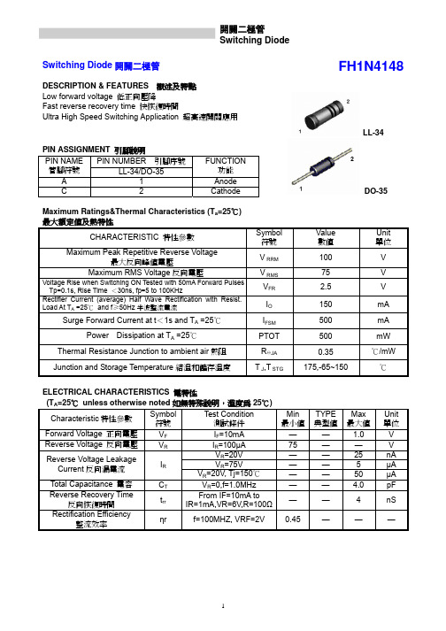
ఎਈऔ!Switching DiodeSwitching Diode ఎਈऔFH1N41481DESCRIPTION & FEATURES 概述及特點Low forward voltage 低正向壓降Fast reverse recovery time 快恢復時間 Ultra High Speed Switching Application 超高速開關應用PIN ASSIGNMENT 引腳說明PIN NUMBER 引腳序號PIN NAME 管腳符號 LL-34/DO-35FUNCTION 功能 A 1 Anode C 2 CathodeLL-34DO-35Maximum Ratings&Thermal Characteristics (T a =25℃) 最大額定值及熱特性CHARACTERISTIC 特性參數 Symbol符號 Value 數值 Unit 單位Maximum Peak Repetitive Reverse Voltage最大反向峰值電壓V RRM 100 V Maximum RMS Voltage 反向電壓V RMS 75 V Voltage Rise when Switching ON Tested with 50mA Forward Pulses Tp=0.1s, Rise Time <30ns, fp=5 to 100KHzV FR 2.5 V Rectifier Current (average) Half Wave Rectification with Resist.Load At T A =25℃ andf ≥50Hz 半波整流電流 I O 150 mA Surge Forward Current at t <1s and T A =25℃I FSM 500 mA Power Dissipation at T A =25℃PTOT 500 mW Thermal Resistance Junction to ambient air 熱阻 R ΘJA0.35℃/mW Junction and Storage Temperature 結溫和儲存溫度T J ,T STG 175,-65~150℃ELECTRICAL CHARACTERISTICS 電特性(T A =25℃ unless otherwise noted 如無特殊說明,溫度為25℃)Characteristic 特性參數Symbol 符號 Test Condition 測試條件 Min 最小值TYPE 典型值 Max 最大值Unit單位Forward Voltage 正向電壓V F I F =10mA — — 1.0 V Reverse Voltage 反向電壓V RI R =100µA 75 — — V V R =20V — — 25 nAV R =75V — — 5 µA Reverse Voltage LeakageCurrent 反向漏電流I RV R =20V, Tj=150℃ — — 50 µATotal Capacitance 電容 C T V R =0,f = 1.0MHz — — 4.0 pF Reverse Recovery Time 反向恢復時間 t rr From IF=10mA toIR=1mA,VR=6V,R=100Ω— — 4 nSRectification Efficiency整流效率ηr f =100MHZ, VRF =2V 0.45 — — —。
1N4148WS / 1N4448WS / 1N914BWS — Small Signal Diodes1N4148WS / 1N4448WS / 1N914BWS — Small Signal Diodes1N4148WS / 1N4448WS / 1N914BWS Small Signal Diodes1N4148WS / 1N4448WS / 1N914BWSRev. I31TRADEMARKSThe following are registered and unregistered trademarks and service marks Fairchild Semiconductor owns or is authorized to use andis not intended to be an exhaustive list of all such trademarks.DISCLAIMERFAIRCHILD SEMICONDUCTOR RESERVES THE RIGHT TO MAKE CHANGES WITHOUT FURTHER NOTICE TO ANY PRODUCTS HEREIN TO IMPROVE RELIABILITY, FUNCTION, OR DESIGN. FAIRCHILD DOES NOT ASSUME ANY LIABILITY ARISING OUT OF THE APPLICATION OR USE OF ANY PRODUCT OR CIRCUIT DESCRIBED HEREIN; NEITHER DOES IT CONVEY ANY LICENSE UNDER ITS PATENT RIGHTS, NOR THE RIGHTS OF OTHERS. THESE SPECIFICATIONS DO NOT EXPAND THE TERMS OF FAIRCHILD’S WORLDWIDE TERMS AND CONDITIONS, SPECIFICALLY THE WARRANTY THEREIN, WHICH COVERS THESE PRODUCTS.LIFE SUPPORT POLICYFAIRCHILD’S PRODUCTS ARE NOT AUTHORIZED FOR USE AS CRITICAL COMPONENTS IN LIFE SUPPORT DEVICES OR SYSTEMS WITHOUT THE EXPRESS WRITTEN APPROVAL OF FAIRCHILD SEMICONDUCTOR CORPORATION.As used herein:1. Life support devices or systems are devices or systemswhich, (a) are intended for surgical implant into the body, or (b) support or sustain life, and (c) whose failure to perform when properly used in accordance with instructions for use provided in the labeling, can be reasonably expected to result in significant injury to the user.2.A critical component is any component of a life support device or system whose failure to perform can be reasonably expected to cause the failure of the life support device or system, or to affect its safety or effectiveness.PRODUCT STATUS DEFINITIONS Definition of Terms ACEx ®Build it Now™CorePLUS™CROSSVOLT ™CTL™Current Transfer Logic™EcoSPARK ®Fairchild ®Fairchild Semiconductor ®FACT Quiet Series™FACT ®FAST ®FastvCore™FPS™FRFET ®Global Power Resource SMGreen FPS™Green FPS™ e-Series™GTO™i-Lo ™IntelliMAX™ISOPLANAR™MegaBuck™MICROCOUPLER™MicroFET™MicroPak™MillerDrive™Motion-SPM™OPTOLOGIC ®OPTOPLANAR ®®PDP-SPM™Power220®Power247®POWEREDGE ®Power-SPM™PowerTrench ®Programmable Active Droop™QFET ®QS™QT Optoelectronics™Quiet Series™RapidConfigure™SMART START™SPM ®STEALTH™SuperFET™SuperSOT™-3SuperSOT™-6SuperSOT™-8SyncFET™The Power Franchise ®TinyBoost™TinyBuck™TinyLogic ®TINYOPTO™TinyPower™TinyPWM™TinyWire™µSerDes™UHC ®UniFET™VCX™Datasheet IdentificationProduct StatusDefinitionAdvance Information Formative or In DesignThis datasheet contains the design specifications for product development. Specifications may change in any manner without notice.Preliminary First ProductionThis datasheet contains preliminary data; supplementary data will be pub-lished at a later date. Fairchild Semiconductor reserves the right to make changes at any time without notice to improve design.No Identification Needed Full ProductionThis datasheet contains final specifications. Fairchild Semiconductor reserves the right to make changes at any time without notice to improve design. Obsolete Not In ProductionThis datasheet contains specifications on a product that has been discontin-ued by Fairchild semiconductor. The datasheet is printed for reference infor-mation only.。
1N4148WT / 1N4448WT / 1N914BWT — High Conductance Fast Switching Diode1N4148WT / 1N4448WT / 1N914BWT — High Conductance Fast Switching Diode Package DimensionSOD-523F1N4148WT / 1N4448WT / 1N914BWT High Conductance Fast Switching Diode1N4148WT / 1N4448WT / 1N914BWTRev. I31TRADEMARKSThe following are registered and unregistered trademarks and service marks Fairchild Semiconductor owns or is authorized to use andis not intended to be an exhaustive list of all such trademarks.DISCLAIMERFAIRCHILD SEMICONDUCTOR RESERVES THE RIGHT TO MAKE CHANGES WITHOUT FURTHER NOTICE TO ANY PRODUCTS HEREIN TO IMPROVE RELIABILITY, FUNCTION, OR DESIGN. FAIRCHILD DOES NOT ASSUME ANY LIABILITY ARISING OUT OF THE APPLICATION OR USE OF ANY PRODUCT OR CIRCUIT DESCRIBED HEREIN; NEITHER DOES IT CONVEY ANY LICENSE UNDER ITS PATENT RIGHTS, NOR THE RIGHTS OF OTHERS. THESE SPECIFICATIONS DO NOT EXPAND THE TERMS OF FAIRCHILD’S WORLDWIDE TERMS AND CONDITIONS, SPECIFICALLY THE WARRANTY THEREIN, WHICH COVERS THESE PRODUCTS.LIFE SUPPORT POLICYFAIRCHILD’S PRODUCTS ARE NOT AUTHORIZED FOR USE AS CRITICAL COMPONENTS IN LIFE SUPPORT DEVICES OR SYSTEMS WITHOUT THE EXPRESS WRITTEN APPROVAL OF FAIRCHILD SEMICONDUCTOR CORPORATION.As used herein:1. Life support devices or systems are devices or systemswhich, (a) are intended for surgical implant into the body, or (b) support or sustain life, and (c) whose failure to perform when properly used in accordance with instructions for use provided in the labeling, can be reasonably expected to result in significant injury to the user.2.A critical component is any component of a life support device or system whose failure to perform can be reasonably expected to cause the failure of the life support device or system, or to affect its safety or effectiveness.PRODUCT STATUS DEFINITIONS Definition of Terms ACEx ®Build it Now™CorePLUS™CROSSVOLT ™CTL™Current Transfer Logic™EcoSPARK ®Fairchild ®Fairchild Semiconductor ®FACT Quiet Series™FACT ®FAST ®FastvCore™FPS™FRFET ®Global Power Resource SMGreen FPS™Green FPS™ e-Series™GTO™i-Lo ™IntelliMAX™ISOPLANAR™MegaBuck™MICROCOUPLER™MicroFET™MicroPak™MillerDrive™Motion-SPM™OPTOLOGIC ®OPTOPLANAR ®®PDP-SPM™Power220®Power247®POWEREDGE ®Power-SPM™PowerTrench ®Programmable Active Droop™QFET ®QS™QT Optoelectronics™Quiet Series™RapidConfigure™SMART START™SPM ®STEALTH™SuperFET™SuperSOT™-3SuperSOT™-6SuperSOT™-8SyncFET™The Power Franchise ®TinyBoost™TinyBuck™TinyLogic ®TINYOPTO™TinyPower™TinyPWM™TinyWire™µSerDes™UHC ®UniFET™VCX™Datasheet IdentificationProduct StatusDefinitionAdvance Information Formative or In DesignThis datasheet contains the design specifications for product development. Specifications may change in any manner without notice.Preliminary First ProductionThis datasheet contains preliminary data; supplementary data will be pub-lished at a later date. Fairchild Semiconductor reserves the right to make changes at any time without notice to improve design.No Identification Needed Full ProductionThis datasheet contains final specifications. Fairchild Semiconductor reserves the right to make changes at any time without notice to improve design. Obsolete Not In ProductionThis datasheet contains specifications on a product that has been discontin-ued by Fairchild semiconductor. The datasheet is printed for reference infor-mation only.。
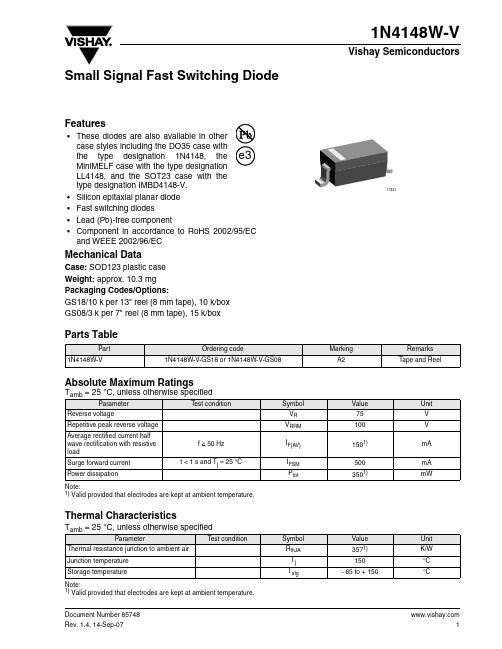
1N4148W-VDocument Number 85748Rev. 1.4, 14-Sep-07Vishay Semiconductors117431Small Signal Fast Switching DiodeFeatures•These diodes are also available in other case styles including the DO35 case withthe type designation 1N4148, the MiniMELF case with the type designation LL4148, and the SOT23 case with the type designation IMBD4148-V. •Silicon epitaxial planar diode •Fast switching diodes•Lead (Pb)-free component•Component in accordance to RoHS 2002/95/EC and WEEE 2002/96/ECMechanical DataCase: SOD123 plastic case Weight: approx. 10.3 mg Packaging Codes/Options:GS18/10 k per 13" reel (8 mm tape), 10 k/box GS08/3 k per 7" reel (8 mm tape), 15 k/boxParts TableAbsolute Maximum RatingsT amb = 25°C, unless otherwise specifiedNote:1)Valid provided that electrodes are kept at ambient temperature.Thermal CharacteristicsT amb = 25°C, unless otherwise specifiedNote:1)Valid provided that electrodes are kept at ambient temperature.PartOrdering codeMarking Remarks 1N4148W-V1N4148W-V-GS18 or 1N4148W-V-GS08A2Tape and ReelParameterT est conditionSymbol Value Unit Reverse voltageV R 75V Repetitive peak reverse voltage V RRM 100V Average rectified current half wave rectification with resistive loadf ≥ 50 Hz I F(AV)1501)mA Surge forward current t < 1 s and T j = 25°CI FSM 500mA Power dissipationP tot3501)mWParameterTest conditionSymbol Value Unit Thermal resistance junction to ambient air R thJA 3571)K/W Junction temperature T j 150°C Storage temperatureT stg- 65 to + 150°C 2Document Number 85748Rev. 1.4, 14-Sep-071N4148W-VVishay Semiconductors Electrical CharacteristicsT amb = 25°C, unless otherwise specifiedRectification Efficiency Measurement CircuitParameterTest condition Symbol MinTyp.Max Unit Forward voltageI F = 10 mA V F 1000mV I F = 100 mA V F 1200mV Leakage currentV R = 20 VI R 25nA V R = 75 V I R 5µA V R = 100 V I R 100µA V R = 20 V , T J = 150°CI R 50µA Diode capacitanceV F = V R = 0 VC D 4pF Voltage rise when switching ON (tested with 50 mA pulses)tested with 50 mA pulses, t p = 0.1 µs, rise time < 30 ns,f p = (5 to 100) kHz V fr 2.5VReverse recovery time I F = 10 mA, I R = 1 mA, V R = 6 V,R L = 100 Ωt rr 4nsRectification efficiencyf = 100 MHz, V RF = 2 Vην0.451N4148W-VDocument Number 85748Rev. 1.4, 14-Sep-07Vishay Semiconductors3Typical CharacteristicsT amb = 25°C, unless otherwise specifiedFigure 1. Forward characteristics Figure 2. Dynamic Forward Resistance vs. Forward Current Figure3. Admissible Power Dissipation vs. Ambient Temperature17437012V F (V )I F (m A )10-110-211010210317438f = 1 kHzT j = 25 °C I F (mA)r f (Ω)1010210310410-210-111021025252525Figure 4. Relative Capacitance vs. Reverse VoltageFigure 5. Leakage Current vs. Junction Temperature17440V R (V )0.70.80.91.01.1f = 1 MHzT j = 25 °C 2086410C D (V R )C D (0 V)17441T j (°C)I R (n A )10102103104100200252525251 4Document Number 85748Rev. 1.4, 14-Sep-071N4148W-VVishay SemiconductorsPackage Dimensions in millimeters (inches): SOD123Figure 6. Admissible Repetitive Peak Forward Current vs. Pulse Duration17442t P (s)I F R M (A )10013510-510-410-31010-110-225252525252524103524135240.11N4148W-VDocument Number 85748Rev. 1.4, 14-Sep-07Vishay Semiconductors5Ozone Depleting Substances Policy StatementIt is the policy of Vishay Semiconductor GmbH to1.Meet all present and future national and international statutory requirements.2.Regularly and continuously improve the performance of our products, processes, distribution and operating systems with respect to their impact on the health and safety of our employees and the public, as well as their impact on the environment.It is particular concern to control or eliminate releases of those substances into the atmosphere which are known as ozone depleting substances (ODSs).The Montreal Protocol (1987) and its London Amendments (1990) intend to severely restrict the use of ODSs and forbid their use within the next ten years. Various national and international initiatives are pressing for an earlier ban on these substances.Vishay Semiconductor GmbH has been able to use its policy of continuous improvements to eliminate the use of ODSs listed in the following documents.1.Annex A, B and list of transitional substances of the Montreal Protocol and the London Amendments respectively2.Class I and II ozone depleting substances in the Clean Air Act Amendments of 1990 by the Environmental Protection Agency (EPA) in the USA3.Council Decision 88/540/EEC and 91/690/EEC Annex A, B and C (transitional substances) respectively.Vishay Semiconductor GmbH can certify that our semiconductors are not manufactured with ozone depleting substances and do not contain such substances.We reserve the right to make changes to improve technical designand may do so without further notice.Parameters can vary in different applications. All operating parameters must be validated for each customer application by the customer. Should the buyer use Vishay Semiconductors products for any unintended or unauthorized application, the buyer shall indemnify Vishay Semiconductors against all claims, costs, damages, and expenses, arising out of, directly or indirectly, any claim of personal damage, injury or death associatedwith such unintended or unauthorized use.Vishay Semiconductor GmbH, P.O.B. 3535, D-74025 Heilbronn, GermanyDocument Number: 91000Revision: 18-Jul-081DisclaimerLegal Disclaimer NoticeVishayAll product specifications and data are subject to change without notice.Vishay Intertechnology, Inc., its affiliates, agents, and employees, and all persons acting on its or their behalf (collectively, “Vishay”), disclaim any and all liability for any errors, inaccuracies or incompleteness contained herein or in any other disclosure relating to any product.Vishay disclaims any and all liability arising out of the use or application of any product described herein or of any information provided herein to the maximum extent permitted by law. The product specifications do not expand or otherwise modify Vishay’s terms and conditions of purchase, including but not limited to the warranty expressed therein, which apply to these products.No license, express or implied, by estoppel or otherwise, to any intellectual property rights is granted by this document or by any conduct of Vishay.The products shown herein are not designed for use in medical, life-saving, or life-sustaining applications unless otherwise expressly indicated. Customers using or selling Vishay products not expressly indicated for use in such applications do so entirely at their own risk and agree to fully indemnify Vishay for any damages arising or resulting from such use or sale. Please contact authorized Vishay personnel to obtain written terms and conditions regarding products designed for such applications.Product names and markings noted herein may be trademarks of their respective owners.元器件交易网。
Features• Fast Switching Speed• Ultra-Small Surface Mount Package• For General Purpose Switching Applications • High Conductance• Lead Free By Design/RoHS Compliant (Note 1)• Qualified to AEC-Q101 Standards for High Reliability •“Green” Device, Notes 4 and 5Mechanical Data• Case: SOD-523• Case Material: Molded Plastic, “Green” Molding Compound, Note 5. UL Flammability Classification Rating 94V-0 • Moisture Sensitivity: Level 1 per J-STD-020D • Terminal Connections: Cathode Band• Terminals: Finish - Matte Tin annealed over Alloy 42 leadframe. Solderable per MIL-STD-202, Method 208 • Marking Information: See Page 2 • Ordering Information: See Page 2 •Weight: 0.0014 grams (approximate)SOD-523TOP VIEWMaximum Ratings @T A = 25°C unless otherwise specifiedCharacteristic Symbol Value UnitNon-Repetitive Peak Reverse Voltage V RM 100 V Reverse Voltage V R 80 V RMS Reverse Voltage V R(RMS) 53 V Forward Continuous Current I FM 250 mA Average Rectified Output Current I O125 mA Non-Repetitive Peak Forward Surge Current @ t = 1.0μs@ t = 100msI FSM2.0 1.0 AThermal CharacteristicsCharacteristic Symbol Value UnitPower Dissipation (Note 2) P D150 mW Thermal Resistance Junction to Ambient Air (Note 2) R θJA 833 °C/W Operating and Storage Temperature Range T J , T STG -65 to +150 °CElectrical Characteristics @T A = 25°C unless otherwise specifiedCharacteristic Symbol Min Max Unit Test Conditions Reverse Breakdown Voltage (Note 3) V (BR)R 75 ⎯ V I R = 1.0μAForward Voltage V F⎯ 0.7150.8551.0 1.25 V I F = 1.0mA I F = 10mA I F = 50mA I F = 150mAPeak Reverse Current (Note 3) I R⎯ 1.050 30 25 μA μAμA nA V R = 75V V R = 75V, T J = 150°C V R = 25V, T J = 150°C V R = 20VTotal Capacitance C T ⎯ 2.0 pF V R = 0, f = 1.0MHzReverse Recovery Time t rr ⎯4.0 ns I F = I R = 10mA,I rr = 0.1 x I R , R L = 100ΩNotes:1. No purposefully added lead.2. Part mounted on FR-4 PC board with recommended pad layout, which can be found on our website at /datasheets/ap02001.pdf.3. Short duration pulse test used to minimize self-heating effect.4. Diodes Inc.'s "Green" policy can be found on our website at /products/lead_free/index.php.5. Product manufactured with Date Code 0627 (week 27, 2006) and newer are built with Green Molding Compound. Product manufactured prior to Date Code 0627 are built with Non-Green Molding Compound and may contain Halogens or Sb2O3 Fire Retardants.5075P , P O W E R D I S S I P A T I O N (m W )D T , AMBIENT TEMPERATURE (C)Fig. 1 Power Derating CurveA °I , I N S T A N T A N E O U S F O R W A R D C U R R E N T (A )F V , INSTANTANEOUS FORWARD VOLTAGE (V)Fig. 2 Typical Forward Characteristics FV , INSTANTANEOUS REVERSE VOLTAGE (V)Fig. 3 Typical Reverse Characteristics R I , I N S T A N T A N E O U S R E V E R S E C U R R E N T (n A )R20C , T O T A L C A P A C I T A N C E (p F )T V , DC REVERSE VOLTAGE (V)Fig. 4 Total Capacitance vs. Reverse Voltage ROrdering Information (Notes 5 & 6)Part NumberCase Packaging 1N4148WT-7SOD-523 3000/Tape & ReelNotes: 6. For packaging details, go to our website at /datasheets/ap02007.pdf.Marking InformationT4Cathode BandT4 = Product Type Marking CodePackage Outline DimensionsSuggested Pad LayoutIMPORTANT NOTICEDiodes Incorporated and its subsidiaries reserve the right to make modifications, enhancements, improvements, corrections or other changes without further notice to any product herein. Diodes Incorporated does not assume any liability arising out of the application or use of any product described herein; neither does it convey any license under its patent rights, nor the rights of others. The user of products in such applications shall assume all risks of such use and will agree to hold Diodes Incorporated and all the companies whose products are represented on our website, harmless against all damages.LIFE SUPPORTDiodes Incorporated products are not authorized for use as critical components in life support devices or systems without the expressed written approval of the President of Diodes Incorporated.SOD-523 Dim Min Max A 1.50 1.70 B 1.10 1.30 C 0.25 0.35 D 0.70 0.90 E 0.10 0.20 G 0.50 0.70 All Dimensions in mmZXCG Y Dimensions Value (in mm)Z 2.3 G 1.1 X 0.8 Y 0.6 C 1.7。
安徽富信半导体科技有限公司ANHUI FOSAN SEMICONDUCTOR TECHNOLOGY CO.,LTD.1N4148WSSOD-323Switching Diode 开关二极管■Features 特点Fast Switching Speed 快的开关速度Surface mount device 表面贴装器件High Conductance 高电导率Case 封装:SOD-323Marking 印字:T4■Maximum Rating 最大额定值(T A =25℃unless otherwise noted 如无特殊说明,温度为25℃)Characteristic 特性参数Symbol 符号Rating 额定值Unit 单位Non-Repetitive Peak Reverse Voltage 不重复反向峰值电压V RM 100V DC Reverse Voltage 直流反向电压V R 75V Peak Repetitive Reverse Voltage 峰值重复反向电压V RRM 75V Woke Peak Reverse Voltage 峰值反向工作电压V RWM 75V RMS Reverse Voltage 反向电压均方根值V R(RMS)53V Forward Rectified Output Current 正向工作电流I O 200mA Non-Repetitive Peak Surge Current@t=1µS 不重复峰值浪涌电流@t=1S I FSM 21A Power Dissipation 耗散功率P D 200mW Thermal Resistance Junction-Ambient 结到环境热阻R θJA 625℃/W Junction/StorageTemperature 结温/储藏温度T J,T stg-50to+150℃℃■Electrical Characteristics 电特性(T A =25℃unless otherwise noted 如无特殊说明,温度为25℃)Characteristic 特性参数Symbol 符号Min 最小值Max 最大值Unit 单位Condition 条件Reverse Voltage 反向电压V R75VI R =1µA Forward Voltage 正向电压V F 0.7150.8551.01.25V I F =1mA I F =10mA I F =50mA I F =150mA Reverse Current 反向电流I R 125µA nA V R =75V V R =20V Junction Capacitance 结电容C J2pFV R =4V,f=1MHz安徽富信半导体科技有限公司ANHUI FOSAN SEMICONDUCTOR TECHNOLOGY CO.,LTD.1N4148WS ■Typical Characteristic Curve典型特性曲线■Dimension外形封装尺寸。
丝印w1二极管参数
丝印W1二极管通常指的是1N4148型号的二极管。
1N4148是一种快速开关二极管,常用于一般目的的快速开关和整流应用。
下面是关于1N4148二极管的一些参数:
1. 最大反向工作电压,1N4148二极管的最大反向工作电压为100V。
这意味着在正向工作时,它可以承受高达100V的反向电压,超过这个电压可能会损坏二极管。
2. 最大连续正向电流,1N4148二极管的最大连续正向电流为300mA。
这意味着在正向工作时,它可以承受高达300mA的电流,超过这个电流可能会损坏二极管。
3. 正向压降,1N4148二极管的正向压降在标准条件下约为
0.7V。
这意味着在正向工作时,它需要至少0.7V的电压才能开始导通。
4. 封装类型,1N4148二极管通常采用小型塑料封装,方便安装和使用。
总的来说,1N4148二极管是一种常用的快速开关二极管,具有较高的反向工作电压和正向电流能力,适用于多种电子电路应用。
希望这些信息能够满足你的需求。