TLE8366 资料
- 格式:doc
- 大小:159.00 KB
- 文档页数:3
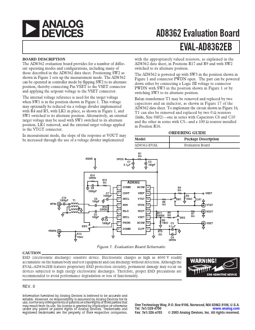
REV.0Information furnished by Analog Devices is believed to be accurate and reliable. However, no responsibility is assumed by Analog Devices for its use, nor for any infringements of patents or other rights of third parties that may result from its use. No license is granted by implication or otherwise unde r any pate nt or pate nt rights of Analog De vice s. Trade marks and re giste re d trade marks are the prope rty of the ir re spe ctive companie s.One Technology Way, P.O. Box 9106, Norwood, MA 02062-9106, U.S.A.Tel: 781/329-4700 Fax: 781/326-8703© 2003 Analog Devices, Inc. All rights reserved.EVAL-AD8362EBAD8362 Evaluation BoardBOARD DESCRIPTIONThe AD8362 evaluation board provides for a number of differ-ent operating modes and configurations, including many of those described in the AD8362 data sheet. Positioning SW2 as shown in Figure 1 sets up the measurement mode. The AD8362can be operated in controller mode by flipping SW2 to its alternate position, thereby connecting Pin VSET to the VSET connector and applying the setpoint voltage to the VSET connector.The internal voltage reference is used for the target voltage when SW1 is in the position shown in Figure 1. This voltage may optionally be reduced via a voltage divider implemented with R4 and R5, with LK1 in place, as shown in Figure 1, and SW1 switched to its alternate position. Alternatively, an external target voltage may be used with SW1 switched to its alternate position, LK1 removed, and the external target voltage applied to the VTGT connector.ESD (electrostatic discharge) sensitive device. Electrostatic charges as high as 4000V readily accumulate on the human body and test equipment and can discharge without detection. Although the EVAL-AD8362EB features proprietary ESD protection circuitry, permanent damage may occur on devices subjected to high energy electrostatic discharges. Therefore, proper ESD precautions are recommended to avoid performance degradation or loss of functionality.with the appropriately valued resistors, as explained in the AD8362 data sheet, in Positions R17 and R9 and with SW2switched to its alternate position.The AD8362 is powered up with SW3 in the position shown in Figure 1 and connector PWDN open. The part can be powered down either by connecting a Logic HI voltage to connector PWDN with SW3 in the position shown in Figure 1 or by switching SW3 to its alternate position.Balun transformer T1 may be removed and replaced by two capacitors and an inductor, as shown in Figure 17 of the AD8362 data sheet. To implement the circuit shown in Figure 16,T1 can also be removed and replaced by two 0 Ω resistors (links, Size 0402)—one in series with Capacitors C6 and C10and the other in series with C5—and a 100 Ω resistor installed in Position R16.REV.0C 03711–0–4/03(0)–2–EVAL-AD8362EBTable I.Evaluation Board Configuration OptionsComponent FunctionPart NumberDefault Value T1ETC1.6-4-2-3C1Supply filtering/decoupling capacitor 0.1 µF C2Supply filtering/decoupling capacitor 100 pF C3Output low-pass filter capacitor0.1 µF C9Output low-pass filter capacitor (normally omitted, not installed)C4, C7, C10Input bias-point decoupling capacitors 1000 pF C5, C6Input signal coupling capacitors 100 pF C8Input high-pass filter capacitor 1000 pFDUTAD8362AD8362ARUR1, R4, R6, R7,R8, R10, R150 ΩR5, R9, R13Optional pull-down resistors 10 k ΩR16(Not installed, see text)100 ΩR17Slope adjustment (not installed, see text)(See text)SW1Internal/external target voltage selectorSW2Measurement mode/controller mode selectorSW3Power-down/enable or external power-down selectorFigure ponent Side Metal of Evaluation BoardFigure ponent Side Silkscreen of Evalua-tion Board。

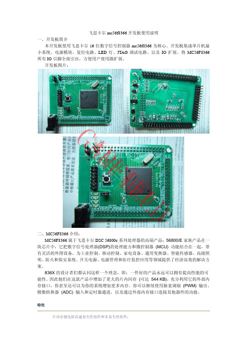
G AR FI EL D飞思卡尔mc56f8366开发板使用说明一、开发板简介本开发板使用飞思卡尔16位数字信号控制器mc56f8366为核心。
开发板集成单片机最小系统、电源模块、复位电路、LED 灯、JTAG 调试电路、以及IO 扩展。
将MC56F8366所有IO 引脚全部引出,方便用户使用跟扩展。
开发板图片:二、MC56F8366介绍:MC56F8366属于飞思卡尔DSC 56800e 系列处理器的高端产品;56800/E 家族产品在一块芯片中,它把数字信号处理器(DSP)的处理能力和微控制器 (MCU) 功能结合在一起,带有灵活的外围设备,为工业控制、移动控制、家电设备、通用变换器、智能传感器、高级照明、防火和保安系统、开关电源、电源管理和医疗监控应用等领域提供了经济高效的解决方案。
836X 的设计者们都认同这样一个理念,即:一件好的产品永远可以拥有提高性能的可能性。
因此他们在这款产品中增加了更大的片内闪存 (可达 544 KB),充分利用它的外部内存接口,你甚至还可以为你的系统增加更多内存。
你可以继续使用脉宽调制 (PWM) 输出、模数转换器 (ADC) 输入和定时器通道,以及通过外部内存接口连接其他器件的功能。
特性片内存储包括高速易失性组件和非易失性组件:G AR F I E L D G AR F I E L DG AR FI EL D512 KB 程序闪存4 KB 程序 RAM (836X 器件) 32 KB 数据 RAM32 KB 数据闪存 (836X 器件) 32 KB 引导闪存存取可配置4MB 片外程序内存和32MB 数据内存 执行频率为60 MHz 时可达60 MIPS芯片选择逻辑适用于连接到 ROM 和 SRAM 的无缝接口 适用于非干扰性、实时调试的 JTAG/EOnCE 4个12位模数转换器 (ADC) 温度传感器可配置2个 FlexCAN (兼容 CAN 版本 2.0 B) 两个串行通信接口 (SCI) 可配置2个串行外围接口 (SPI) 2个专用的外部中断引脚 软件可编程,锁相环可配置76个通用I/O 引脚三、开发板使用说明1、 电源模块开发板上设有电源稳压电路。
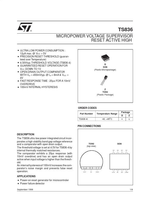
TS836MICROPOWER VOLTAGE SUPERVISORRESET ACTIVE HIGHSeptember 1998D SO8(Plastic Micropackage)®.ULTRA LOW POWER CONSUMPTION :12µA max.@V CC =5V.PRECISION RESET THRESHOLD (guaran-teed over Temperature).4.50Vtyp.THRESHOLD VOLTAGE (TS836-4).GUARANTEED RESET OPERATION FOR V CC DOWN TO 1V.OPEN DRAIN OUTPUT COMPARATOR WITH V ol =450mVtyp.@I ol =8mA &V CC =4V.FAST RESPONSE TIME :20µs FOR A 10mV OVERDRIVE.100mV INTERNAL HYSTERESISDESCRIPTIONThe TS836ultra low power integrated circuit incor-porates a high stability band gap voltage reference and a comparator with open drain output.The threshold voltage is set at 4.5V for TS836-4by internal thermally matched resistances.The comparator exhibits a 20µs response (with 10mV overdrive)and has an open drain output active when input voltage is higher than the thresh-old.An internalhysteresisof 100mVincreases thecom-parator’s noise margin and prevents false reset operation.APPLICATIONS.Power-on reset generator for microcontroler .Power failure detectorORDER CODESPart Number Temperature RangePackage D Z TS836-4I-40,+85oC•ùZ TO92(Plastic Package)PIN CONNECTIONS123OUT IN GNDTO92(top view)87651234NC NC NC OUT IN NC GNDNC SO81/8OPERATING CONDITIONSSymbol ParameterValue Unit V CCSupply Voltage1to 5.5VABSOLUTE MAXIMUM RATINGSSymbol ParameterValue Unit V CC Supply Voltage -note 17V V out Output Voltage -0.3to V CC +0.3V I out Output Current 20mA Pd Power Dissipation200mWT oper Operating Free Air Temperature Range -40to +85o C T stgStorage Temperature-65to +150oCNote:1.All voltages values,except differential voltage are with respect to network ground terminal.TS836-4ELECTRICAL CHARACTERISTICS T amb =25o C (unless otherwise specified)Symbol ParameterMin.Typ.Max.Unit V thi Threshold Voltage -V CC IncreasingT min.≤T amb ≤T max. 4.17 4.5 4.66V V thd Threshold Voltage -V CC DecreasingT min.≤T amb ≤T max. 4.17 4.4 4.66V V hys Hysteresis Voltage 50100200mV I CC Current ConsumptionV CC =5V 12µA V OL Low Level Output VoltageV CC =4V I OL =8mA,T min.≤T amb ≤T max.4508001000mV I OH Output Off-state LeakageV CC =5VT min.≤T amb ≤T max.21001000nA tphlResponse Time High to LowR L =10k Ω,C L =15pF,V CC =V thd -10mV20µsTS8362/8TS836 EQUIVALENT SCHEMATIC DIAGRAMTIMING DIAGRAM3/8-50-40-30-20-1001020304050607080901001101204,44,444,484,524,56Temper atur e (°C)Vthi (Volts)V th i ma xV th i m i nTS836-4Vth vs Temperature while V CC increasing-50-40-30-20-1001020304050607080901001101204,324,344,364,384,44,424,44Temperature (°C)Vthd (Volts)V t h dm ax V t hdm i n TS836-4Vth vs Temperature while V CC decreasing-50-40-30-20-101020304050607080901001101208,28,48,68,899,29,49,6Temperature (°C)Icc (µA)I c cm inI c cm a xTS836-4I CC vs Temperature-50-40-30-20-1001020304050607080901001101206080100120140160Temperature (°C)Hysteresis (mV)TS836-4Hysteresis vs Temperature 4,34,44,54,6012345Input voltage (V)Outputvoltage (V)TS836-4RL=10Kohms T=25°CReset Output Voltage vs Input Voltage 024681012141618200,20,40,60,81Isink (mA)Vol (Volts)TS836-4T=25°CVoltage Output Low vs Sink CurrentTS8364/8Input signal 2V/div 0.5ms/divReset output 2V/div 0.5ms/div0V 5V0V5VTS836-4RL=10Kohms T=25°CReset Output Voltage vs Input Voltage5V3.5V3.5V0VInput signal 0.5V/di v 10µs/di vReset output 2V/div 10µs/divTS836-4RL=10KohmsT=25°CSupply Falling down :Reset Delay TimeIn put signal 0.5V/di v 0.5µs/divReset output 2V/div 0.5µs/div3.5V 5V5V0VTS836-4RL=10KohmsT=25°CSupply Rising up :Output Delay TimeInput sig nal 0.5V/div 0.1ms/divReset output 2V/div 0.1ms/div3.5V5V3.5V0VTS836-4RL=10Kohms CL=10nF T=25°CSupply Falling down :Extended Reset Delay Time with an Additional CapacitorIn put signal 2V/div 0.5ms/divReset output 2V/div 0.5ms/div4V6V 6V0VTS836-4RL=10KohmsT=25°CReset Output Voltage vs Input Voltage (example)3V5V5V0VInput signal 2V/div 0.5ms/divReset output 2V/div 0.5ms/divTS836-4RL=10KohmsT=25°CReset Output Voltage vs Input Voltage (example)TS8365/8TS836Load ResistorInput VoltageOutput VoltageVccResetBasic ConfigurationTS836Load ResistorInput VoltageOutput VoltageVccResetCapacitive LoadConfiguration with an additional Capacitive LoadTS8366/8PACKAGE MECHANICAL DATA8PINS-PLASTIC MICROPACKAGE(SO)Dim.Millimeters InchesMin.Typ.Max.Min.Typ.Max.A 1.750.069a10.10.250.0040.010a2 1.650.065a30.650.850.0260.033b0.350.480.0140.019b10.190.250.0070.010C0.250.50.0100.020c145o(typ.)D 4.8 5.00.1890.197E 5.8 6.20.2280.244e 1.270.050e3 3.810.150F 3.8 4.00.1500.157L0.4 1.270.0160.050M0.60.024S8o(max.)TS8367/8Information furnished is believed to be accurate and reliable.However,STMicroelectronics assumes no responsibility for the consequences of use of such information nor for any infringement of patents or other rights of third parties which may result from its use.No license is granted by implication or otherwise under any patent or patent rights of STMicroelectronics.Specifications mentioned in this publ ication are subject to change without notice.This publication supersedes and replaces all information previously supplied.STMicroelectronics products arenot authorized for useas critical components in life support devices or systems without express written approval of STMicroelectronics.©The ST logo is a trademark of STMicroelectronics©1998STMicroelectronics –Printed in Italy –All Rights ReservedSTMicroelectronics GROUP OF COMPANIESAustralia -Brazil -Canada -China -France -Germany -Italy -Japan -Korea -Malaysia -Malta -Mexico -MoroccoThe Netherlands -Singapore -Spain -Sweden -Switzerland -Taiwan -Thailand -United Kingdom -U.S.A.PACKAGE MECHANICAL DATA 3PINS -PLASTIC PACKAGE TO92limetersInches Min.Typ.Max.Min.Typ.Max.L 1.270.05B 3.2 3.7 4.20.1260.14570.1654O1 4.45 5.00 5.20.17520.19690.2047C 4.58 5.035.330.18030.1980.2098K 12.70.5O20.4070.50.5080.0160.01970.02a0.350.0138TS8368/8。
CHA1P/CHA3CHA1N/CHA2CHA0P/CHA1CHA0N/CHA0CMACHB1P/CHB3CHB1N/CHB2CHB0P/CHB1CHB0N/CHB0CMBCSCLOCKBUSYSDIRDSDOASDOBM0M1CONVSTAGND DGNDRGNDREFIO1REFIO2ADS8363ADS7263ADS7223 SBAS523B–OCTOBER2010–REVISED JANUARY2011 Dual,1MSPS,16-/14-/12-Bit,4×2or2×2Channel,Simultaneous SamplingAnalog-to-Digital ConverterCheck for Samples:ADS8363,ADS7263,ADS7223FEATURES DESCRIPTION•Eight Pseudo-or Four Fully-Differential Inputs The ADS8363is a dual,16-bit,1MSPSanalog-to-digital converter(ADC)with eight pseudo-•Simultaneous Sampling of Two Channelsor four fully-differential input channels grouped into •Excellent AC Performance:two pairs for simultaneous signal acquisition.The –SNR:analog inputs are maintained differentially to the input 93dB(ADS8363)of the ADC.The input multiplexer can be used in 85dB(ADS7263)either pseudo-differential mode,supporting up to four 73dB(ADS7223)channels per ADC(4x2),or in fully-differential modethat allows to convert up to two inputs per ADC(2x2).–THD:The ADS7263is a14-bit version while the ADS7223–98dB(ADS8363)is a12-bit version of the ADS8363.–92dB(ADS7263)–86dB(ADS7223)The ADS8363/7263/7223offer two programmablereference outputs,flexible supply voltage ranges,a •Dual Programmable and Buffered2.5Vprogrammable auto-sequencer,data storage of up to Reference Allows:four conversion results per channel,and several –Two Different Input Voltage Range Settings power-down features.–Two-Level PGA ImplementationAll devices are offered in a5x5mm QFN-32package.•Programmable Auto-Sequencer•Integrated Data Storage(up to4per channel)Functional Block Diagram for Oversampling Applications•2-Bit Counter for Safety Applications•Fully Specified over the Extended IndustrialTemperature RangeAPPLICATIONS•Motor Control:Current and PositionMeasurement including Safety Applications•Power Quality Measurement•Three-Phase Power Control•Programmable Logic Controllers•Industrial Automation•Protection RelaysPlease be aware that an important notice concerning availability,standard warranty,and use in critical applications of TexasInstruments semiconductor products and disclaimers thereto appears at the end of this data sheet.All trademarks are the property of their respective owners.PRODUCTION DATA information is current as of publication date.Copyright©2010–2011,Texas Instruments Incorporated Products conform to specifications per the terms of the TexasADS8363ADS7263ADS7223SBAS523B–OCTOBER2010–REVISED This integrated circuit can be damaged by ESD.Texas Instruments recommends that all integrated circuits be handled with appropriate precautions.Failure to observe proper handling and installation procedures can cause damage.ESD damage can range from subtle performance degradation to complete device failure.Precision integrated circuits may be more susceptible to damage because very small parametric changes could cause the device not to meet its published specifications.ORDERING INFORMATIONFor the most current package and ordering information,see the Package Option Addendum at the end of this document,or visit the device product folder at .FAMILY OVERVIEWPRODUCT RESOLUTION NMC INL SNR THDADS836316bits16or15bits(1)±3or±4LSB(1)93dB(typ)–98dB(typ) ADS726314bits14bits±1LSB85dB(typ)–92dB(typ) ADS722312bits12bits±0.5LSB73dB(typ)–86dB(typ) (1)See Electrical Characteristics.ABSOLUTE MAXIMUM RATINGS(1)Over operating free-air temperature range,unless otherwise noted.ADS8363,ADS7263,ADS7223UNIT Supply voltage,AVDD to AGND or DVDD to DGND–0.3to+6VSupply voltage,DVDD to AVDD 1.2×AVDD(2)VAnalog and reference input voltage with respect to AGND AGND–0.3to AVDD+0.3VDigital input voltage with respect to DGND DGND–0.3to DVDD+0.3VGround voltage difference|AGND-DGND|0.3VInput current to any pin except supply pins–10to+10mA Maximum virtual junction temperature,T J+150°CHuman body model(HBM),±2000V Electrostatic JEDEC standard22,test method A114-C.01discharge(ESD)Charged device model(CDM),ratings,all pins±500V JEDEC standard22,test method C101(1)Stresses above these ratings may cause permanent damage to the device.These are stress ratings only,and functional operation of thedevice at these or any other conditions beyond those specified is not implied.Exposure to absolute maximum conditions for extended periods may affect device reliability.(2)Exceeding the specified limit causes an increase of the DVDD leakage current and leads to malfunction of the device.THERMAL INFORMATIONADS8363,ADS7263,ADS7223THERMAL METRIC(1)UNITSRHB32PINSq JA Junction-to-ambient thermal resistance33.3q JCtop Junction-to-case(top)thermal resistance29.5q JB Junction-to-board thermal resistance7.3°C/Wy JT Junction-to-top characterization parameter0.2y JB Junction-to-board characterization parameter7.4q JCbot Junction-to-case(bottom)thermal resistance0.9(1)For more information about traditional and new thermal metrics,see the IC Package Thermal Metrics application report,SPRA953.2Submit Documentation Feedback Copyright©2010–2011,Texas Instruments IncorporatedADS8363ADS7263ADS7223 SBAS523B–OCTOBER2010–REVISED JANUARY2011 ELECTRICAL CHARACTERISTICS:ADS8363All minimum/maximum specifications at T A=–40°C to+125°C,specified supply voltage range,VREF=2.5V(int),and t DATA= 1MSPS,unless otherwise noted.Typical values are at T A=+25°C,AVDD=5V,and DVDD=3.3V.ADS8363PARAMETER TEST CONDITIONS MIN TYP MAX UNIT RESOLUTION16BitsDC ACCURACYHalf-clock mode–3±1.2+3LSB INL Integral nonlinearityFull-clock mode–4±1.5+4LSBHalf-clock mode–0.99±0.6+2LSB DNL Differential nonlinearityFull-clock mode–1.5±0.8+3LSBV OS Input offset error–2±0.2+2mV V OS match ADC to ADC–1±0.1+1mVdV OS/dT Input offset thermal drift1m V/°CReferenced to the voltage atG ERR Gain error–0.1±0.01+0.1%REFIOxG ERR match ADC to ADC–0.1±0.005+0.1%Referenced to the voltage atG ERR/dT Gain error thermal drift1ppm/°CREFIOxCMRR Common-mode rejection ratio Both ADCs,dc to100kHz92dBAC ACCURACYSINAD Signal-to-noise+distortion V IN=5V PP at10kHz8992dB SNR Signal-to-noise ratio V IN=5V PP at10kHz9093dB THD Total harmonic distortion V IN=5V PP at10kHz–98–90dB SFDR Spurious-free dynamic range V IN=5V PP at10kHz90100dB ELECTRICAL CHARACTERISTICS:ADS7263All minimum/maximum specifications at T A=–40°C to+125°C,specified supply voltage range,VREF=2.5V(int),and t DATA= 1MSPS,unless otherwise noted.Typical values are at T A=+25°C,AVDD=5V,and DVDD=3.3V.ADS7263PARAMETER TEST CONDITIONS MIN TYP MAX UNIT RESOLUTION14BitsDC ACCURACYINL Integral nonlinearity–1±0.4+1LSB DNL Differential nonlinearity–0.5±0.2+1LSBV OS Input offset error–2±0.2+2mV V OS match ADC to ADC–1±0.1+1mVdV OS/dT Input offset thermal drift1m V/°CReferenced to the voltage atG ERR Gain error–0.1±0.01+0.1%REFIOxG ERR match ADC to ADC–0.1±0.005+0.1%Referenced to the voltage atG ERR/dT Gain error thermal drift1ppm/°CREFIOxCMRR Common-mode rejection ratio Both ADCs,dc to100kHz92dBAC ACCURACYSINAD Signal-to-noise+distortion V IN=5V PP at10kHz8284dB SNR Signal-to-noise ratio V IN=5V PP at10kHz8485dB THD Total harmonic distortion V IN=5V PP at10kHz–92–88dB SFDR Spurious-free dynamic range V IN=5V PP at10kHz8892dBCopyright©2010–2011,Texas Instruments Incorporated Submit Documentation Feedback3ADS8363ADS7263ADS7223SBAS523B–OCTOBER2010–REVISED ELECTRICAL CHARACTERISTICS:ADS7223All minimum/maximum specifications at T A=–40°C to+125°C,specified supply voltage range,VREF=2.5V(int),and t DATA= 1MSPS,unless otherwise noted.Typical values are at T A=+25°C,AVDD=5V,and DVDD=3.3V.ADS7223PARAMETER TEST CONDITIONS MIN TYP MAX UNIT RESOLUTION12BitsDC ACCURACYINL Integral nonlinearity–0.5±0.2+0.5LSB DNL Differential nonlinearity–0.5±0.1+0.5LSBV OS Input offset error–2±0.2+2mV V OS match ADC to ADC–1±0.1+1mVdV OS/dT Input offset thermal drift1m V/°CReferenced to the voltage atG ERR Gain error–0.1±0.01+0.1%REFIOxG ERR match ADC to ADC–0.1±0.005+0.1%Referenced to the voltage atG ERR/dT Gain error thermal drift1ppm/°CREFIOxCMRR Common-mode rejection ratio Both ADCs,dc to100kHz92dBAC ACCURACYSINAD Signal-to-noise+distortion V IN=5V PP at10kHz7172dB SNR Signal-to-noise ratio V IN=5V PP at10kHz7273dB THD Total harmonic distortion V IN=5V PP at10kHz–86–84dB SFDR Spurious-free dynamic range V IN=5V PP at10kHz8486dB ELECTRICAL CHARACTERISTICS:GENERALAll minimum/maximum specifications at T A=–40°C to+125°C,specified supply voltage range,VREF=2.5V(int),and t DATA= 1MSPS,unless otherwise noted.Typical values are at T A=+25°C,AVDD=5V,and DVDD=3.3V.ADS8363,ADS7263,ADS7223PARAMETER TEST CONDITIONS MIN TYP MAX UNIT ANALOG INPUT(CHxxP–CHxxN)or CHxx toFSR Full-scale input range–V REF+V REF VCMxV IN Absolute input voltage CHxxx to AGND–0.1AVDD+0.1VC IN Input capacitance CHxxx to AGND45pFC ID Differential input capacitance22.5pFI IL Input leakage current–1616nA PSRR Power-supply rejection ratio AVDD=5.5V75dB SAMPLING DYNAMICSHalf-clock mode17.5t CLKt CONV Conversion time per ADCFull-clock mode35t CLKHalf-clock mode2t CLKt ACQ Acquisition timeFull-clock Mode4t CLKf DATA Data rate251000kSPSt A Aperture delay6ns t A match ADC to ADC50pst AJIT Aperture jitter50psHalf-clock mode0.520MHzf CLK Clock frequencyFull-clock mode140MHzHalf-clock mode502000nst CLK Clock periodFull-clock mode251000ns4Submit Documentation Feedback Copyright©2010–2011,Texas Instruments IncorporatedADS8363ADS7263ADS7223 SBAS523B–OCTOBER2010–REVISED JANUARY2011 ELECTRICAL CHARACTERISTICS:GENERAL(continued)All minimum/maximum specifications at T A=–40°C to+125°C,specified supply voltage range,VREF=2.5V(int),and t DATA= 1MSPS,unless otherwise noted.Typical values are at T A=+25°C,AVDD=5V,and DVDD=3.3V.ADS8363,ADS7263,ADS7223PARAMETER TEST CONDITIONS MIN TYP MAX UNIT INTERNAL VOLTAGE REFERENCEResolution Reference output DAC resolution10BitsOver20%to100%DAC range0.2V REFOUT V REFOUT VV REFOUT Reference output voltage REFIO1,DAC=3FFh, 2.485 2.500 2.515VREFIO2,DAC=3FFh 2.480 2.500 2.520VdV REFOUT/dT Reference voltage drift±10ppm/°C DNL DAC DAC differential linearity error–4±14LSB INL DAC DAC integral linearity error–4±0.54LSBV OSDAC DAC offset error V REFOUT=0.5V–4±14LSB PSRR Power-supply rejection ratio73dBI REFOUT Reference output dc current–2+2mAReference output short-circuitI REFSC50mAcurrent(1)t REFON Reference output settling time C REF=22m F8ms VOLTAGE REFERENCE INPUTV REF Reference input voltage range0.5 2.5 2.525VI REF Reference input current50m AExternal ceramic referenceC REF22m FcapacitanceDIGITAL INPUTS(2)I IN Input current V IN=DVDD to DGND–50+50nAC IN Input capacitance5pFLogic family CMOS with Schmitt-TriggerV IH High-level input voltage DVDD=4.5V to5.5V0.7DVDD DVDD+0.3VV IL Low-level input voltage DVDD=4.5V to5.5V–0.30.3DVDD V Logic family LVCMOSV IH High-level input voltage DVDD=2.3V to3.6V2DVDD+0.3VV IL Low-level input voltage DVDD=2.3V to3.6V–0.30.8V DIGITAL OUTPUTS(2)VC OUT Output capacitance5pFC LOAD Load capacitance30pFLogic family CMOSV OH High-level output voltage DVDD=4.5V,I OH=–100µA 4.44VV OL Low-level output voltage DVDD=4.5V,I OH=+100µA0.5V Logic family LVCMOSV OH High-level output voltage DVDD=2.3V,I OH=–100µA DVDD–0.2VV OL Low-level output voltage DVDD=2.3V,I OH=+100µA0.2V(1)Reference output current is not internally limited.(2)Specified by design;not production tested.Copyright©2010–2011,Texas Instruments Incorporated Submit Documentation Feedback5ADS8363ADS7263ADS7223SBAS523B–OCTOBER2010–REVISED ELECTRICAL CHARACTERISTICS:GENERAL(continued)All minimum/maximum specifications at T A=–40°C to+125°C,specified supply voltage range,VREF=2.5V(int),and t DATA= 1MSPS,unless otherwise noted.Typical values are at T A=+25°C,AVDD=5V,and DVDD=3.3V.ADS8363,ADS7263,ADS7223PARAMETER TEST CONDITIONS MIN TYP MAX UNITPOWER SUPPLYAVDD to AGND,half-clock mode 2.7 5.0 5.5V AVDD Analog supply voltageAVDD to AGND,full-clock mode 4.5 5.0 5.5V3V and3.3V levels 2.3 2.5 3.6V DVDD Digital supply voltage5V levels,half-clock mode only 4.5 5.0 5.5VAVDD=3.6V12.016.0mAAVDD=5.5V15.020.0mAAVDD=3.6V,sleep/auto-sleep0.8 1.2mA AIDD Analog supply current modesAVDD=5.5V,sleep/auto-sleep0.9 1.4mAmodesPower-down mode0.005mADVDD=3.6V,C LOAD=10pF 1.1 2.5mA DIDD Digital supply currentDVDD=5.5V,C LOAD=10pF36mAAVDD=DVDD=3.6V47.266.6mW Power dissipation(normalP Doperation)AVDD=5.5V,DVDD=3.6V86.5117.0mW6Submit Documentation Feedback Copyright©2010–2011,Texas Instruments IncorporatedCHB1P/CHB3 CHB1N/CHB2 CHB0P/CHB1 CHB0N/CHB0 CHA1P/CHA3 CHA1N/CHA2 CHA0P/CHA1 CHA0N/CHA0SDOBBUSYCLOCKCSRDCONVSTSDIM0123456782423222120191817ADS8363ADS7263ADS7223(Thermal Pad)CMBCMAAGNDAVDDDGNDDVDDNCSDOA32REFIO1931REFIO21030RGND1129AGND1228AVDD1327NC1426NC1525M116ADS8363ADS7263ADS7223 SBAS523B–OCTOBER2010–REVISED JANUARY2011PIN CONFIGURATIONRHB PACKAGEQFN-32(TOP VIEW)Pin DescriptionsPINNAME NO.TYPE(1)DESCRIPTIONCHB1P/CHB31AI Fully-differential noninverting analog input channel B1or pseudo-differential input B3CHB1N/CHB22AI Fully-differential inverting analog input channel B1or pseudo-differential input B2CHB0P/CHB13AI Fully-differential noninverting analog input channel B0or pseudo-differential input B1CHB0N/CHB04AI Fully-differential inverting analog input channel B0or pseudo-differential input B0CHA1P/CHA35AI Fully-differential noninverting analog input channel A1or pseudo-differential input A3CHA1N/CHA26AI Fully-differential inverting analog input channel A1or pseudo-differential input A2CHA0P/CHA17AI Fully-differential nonInverting analog input channel A1or pseudo-differential input A1CHA0N/CHA08AI Fully-differential inverting analog input channel A1or pseudo-differential input A0 REFIO19AIO Reference voltage input/output1.A ceramic capacitor of22µF connected to RGND is required.REFIO210AIO Reference voltage input/output2.A ceramic capacitor of22µF connected to RGND is required.RGND11P Reference ground.Connect to analog ground plane with a dedicated via.AGND12,30P Analog ground.Connect to analog ground plane.AVDD13,29P Analog power supply,2.7V to5.5V.Decouple to AGND with a1m F ceramic capacitor.14,NC NC This pin is not internally connected.15,26M116DI Mode pin1.Selects the digital output mode(see Table4).M017DI Mode pin0.Selects analog input channel mode(see Table4).Serial data input.This pin is used to set up of the internal registers,and can also be used in SDI18DIADS8361-compatible manner.The data on SDI are ignored when CS is high.Conversion start.The ADC switches from sample into hold mode on the rising edge of CONVST.CONVST19DIThereafter,the conversion starts with the next rising edge of the CLOCK pin.Read data.Synchronization pulse for the SDOx outputs and SDI input.RD only triggers when CS is RD20DIlow.(1)AI=analog input,AIO=analog input/output,DI=digital input,DO=digital output,DIO=digital input/output,P=power supply,NC=not connected.Copyright©2010–2011,Texas Instruments Incorporated Submit Documentation Feedback7ADS8363ADS7263ADS7223SBAS523B–OCTOBER2010–REVISED Pin Descriptions(continued)PINNAME NO.TYPE(1)DESCRIPTIONChip select.When this pin is low,the SDOx,SDI,and RD pins are active;when this pin is high,the CS21DISDOx outputs are3-stated,while the SDI and RD inputs are ignored.External clock input.The range is0.5MHz to20MHz in half-clock mode,or1MHz to40MHz in CLOCK22DIfull-clock mode.Converter busy indicator.BUSY goes high when the inputs are in hold mode and returns to low after BUSY23DOthe conversion is complete.SDOB24DO Serial data output for converter B.Active only if M1is low.3-state when CS is high.SDOA25DO Serial data output for converter A.3-state when CS is high.DVDD27P Digital supply,2.3V to5.5V.Decouple to DGND with a1m F ceramic capacitor.DGND28P Digital ground.Connect to digital ground plane.CMA31AI Common-mode voltage input for channels Ax(in pseudo-differential mode only).CMB32AI Common-mode voltage input for channels Bx(in pseudo-differential mode only).8Submit Documentation Feedback Copyright©2010–2011,Texas Instruments IncorporatedADS8363ADS7263ADS7223 SBAS523B–OCTOBER2010–REVISED JANUARY2011 TIMING DIAGRAMS Array(1)The ADS7263/7223output data with the MSB located as ADS8363and last2/4bits being'0'.Figure1.Detailed Timing Diagram:Half-Clock Mode(ADS8361-Compatible)Copyright©2010–2011,Texas Instruments Incorporated Submit Documentation Feedback9ADS8363ADS7263ADS7223SBAS523B–OCTOBER2010–REVISED Array(2)The ADS7263/7223output data with the MSB located as ADS8363and last2/4bits being'0'.Figure2.Detailed Timing Diagram:Full-Clock Mode10Submit Documentation Feedback Copyright©2010–2011,Texas Instruments Incorporated分销商库存信息:TIADS8363SRHBT ADS8363SRHBR。
TLE4966-2KHigh Precision Hall Switch with two OutputsDatasheetRev.1.0, 2010-06-28Edition 2010-06-28Published byInfineon Technologies AG81726 Munich, Germany© 2010Infineon Technologies AGAll Rights Reserved.Legal DisclaimerThe information given in this document shall in no event be regarded as a guarantee of conditions or characteristics. With respect to any examples or hints given herein, any typical values stated herein and/or any information regarding the application of the device, Infineon Technologies hereby disclaims any and all warranties and liabilities of any kind, including without limitation, warranties of non-infringement of intellectual property rights of any third party.InformationFor further information on technology, delivery terms and conditions and prices, please contact the nearest Infineon Technologies Office ().WarningsDue to technical requirements, components may contain dangerous substances. For information on the types in question, please contact the nearest Infineon Technologies Office.Infineon Technologies components may be used in life-support devices or systems only with the express written approval of Infineon Technologies, if a failure of such components can reasonably be expected to cause the failure of that life-support device or system or to affect the safety or effectiveness of that device or system. Life support devices or systems are intended to be implanted in the human body or to support and/or maintain and sustain and/or protect human life. If they fail, it is reasonable to assume that the health of the user or other persons may be endangered.TLE4966-2KRevision History: 2010-06-28, Rev.1.0Previous Revision:Page Subjects (major changes since last revision)Trademarks of Infineon Technologies AGABM™, BlueMoon™, CONVERGATE™, COSIC™, C166™, FALC™, GEMINAX™, GOLDMOS™, ISAC™, OMNITUNE™, OMNIVIA™, PROSOC™, SEROCCO™, SICOFI™, SIEGET™, SMARTi™, SMINT™, SOCRATES™, VINAX™, VINETIC™, VOIPRO™, X-GOLD™, XMM™, X-PMU™, XWAY™Other TrademarksMicrosoft®, Visio®, Windows®, Windows Vista®, Visual Studio®, Win32® of Microsoft Corporation. Linux® of Linus Torvalds. FrameMaker®, Adobe® Reader™, Adobe Audition® of Adobe Systems Incorporated. APOXI®, COMNEON™ of Comneon GmbH & Co. OHG. PrimeCell®, RealView®, ARM®, ARM® Developer Suite™ (ADS), Multi-ICE™, ARM1176JZ-S™, CoreSight™, Embedded Trace Macrocell™ (ETM), Thumb®, ETM9™, AMBA™, ARM7™, ARM9™, ARM7TDMI-S™, ARM926EJ-S™ of ARM Limited. OakDSPCore®, TeakLite® DSP Core, OCEM® of ParthusCeva Inc. IndoorGPS™, GL-20000™, GL-LN-22™ of Global Locate. mipi™ of MIPI Alliance. CAT-iq™ of DECT Forum. MIPS™, MIPS II™, 24KEc™, MIPS32®, 24KEc™ of MIPS Technologies, Inc. Texas Instruments®, PowerPAD™, C62x™, C55x™, VLYNQ™, Telogy Software™, TMS320C62x™, Code Composer Studio™, SSI™ of Texas Instruments Incorporated. Bluetooth® of Bluetooth SIG, Inc. IrDA® of the Infrared Data Association. Java™, SunOS™, Solaris™ of Sun Microsystems, Inc. Philips®, I2C-Bus® of Koninklijke Philips Electronics N.V. Epson® of Seiko Epson Corporation. Seiko® of Kabushiki Kaisha Hattori Seiko Corporation. Panasonic® of Matsushita Electric Industrial Co., Ltd. Murata® of Murata Manufacturing Company. Taiyo Yuden™of Taiyo Yuden Co., Ltd. TDK® of TDK Electronics Company, Ltd. Motorola® of Motorola, Inc. National Semiconductor®, MICROWIRE™ of National Semiconductor Corporation. IEEE® of The Institute of Electrical and Electronics Engineers, Inc. Samsung®, OneNAND®, UtRAM® of Samsung Corporation. Toshiba® of Toshiba Corporation. Dallas Semiconductor®, 1-Wire® of Dallas Semiconductor Corp. ISO® of the International Organization for Standardization. IEC™ of the International Engineering Consortium. EMV™ of EMVCo, LLC. Zetex® of Zetex Semiconductors. Microtec® of Microtec Research, Inc. Verilog® of Cadence Design Systems, Inc. ANSI® of the American National Standards Institute, Inc. WindRiver® and VxWorks® of Wind River Systems, Inc. Nucleus™ of Mentor Graphics Corporation. OmniVision® of OmniVision Technologies, Inc. Sharp® of Sharp Corporation. Symbian OS® of Symbian Software Ltd. Openwave® of Openwave Systems, Inc. Maxim® of Maxim Integrated Products, Inc. Spansion® of Spansion LLC. Micron®, CellularRAM® of Micron Technology, Inc. RFMD® of RF Micro Devices, Inc. EPCOS® of EPCOS AG. UNIX® of The Open Group. Tektronix® of Tektronix, Inc. Intel® of Intel Corporation. Qimonda® of Qimonda AG. 1GOneNAND® of Samsung Corporation. HyperTerminal® of Hilgraeve, Inc. MATLAB® of The MathWorks, Inc. Red Hat® of Red Hat, Inc. Palladium® of Cadence Design Systems, Inc. SIRIUS Satellite Radio® of SIRIUS Satellite Radio Inc. TOKO® of TOKO Inc.The information in this document is subject to change without notice.Last Trademarks Update 2008-11-17Trademarks of Infineon Technologies AG . . . . . . . . . . . . . . . . . . . . . . 31Overview . . . . . . . . . . . . . . . . . . . . . . . . . . . . . . . . . . . . . . . . . . . . . . . . . . . 5 1.1Features . . . . . . . . . . . . . . . . . . . . . . . . . . . . . . . . . . . . . . . . . . . . . . . . . . . . 5 1.2Functional Description . . . . . . . . . . . . . . . . . . . . . . . . . . . . . . . . . . . . . . . . . 5 1.3Pin Configuration (top view) . . . . . . . . . . . . . . . . . . . . . . . . . . . . . . . . . . . . . 62General . . . . . . . . . . . . . . . . . . . . . . . . . . . . . . . . . . . . . . . . . . . . . . . . . . . . 7 2.1Block Diagram . . . . . . . . . . . . . . . . . . . . . . . . . . . . . . . . . . . . . . . . . . . . . . . 7 2.2Circuit Description . . . . . . . . . . . . . . . . . . . . . . . . . . . . . . . . . . . . . . . . . . . . 7 2.3Application Circuit . . . . . . . . . . . . . . . . . . . . . . . . . . . . . . . . . . . . . . . . . . . . 8 3Maximum Ratings . . . . . . . . . . . . . . . . . . . . . . . . . . . . . . . . . . . . . . . . . . . 84Operating Range . . . . . . . . . . . . . . . . . . . . . . . . . . . . . . . . . . . . . . . . . . . . 95Electrical and Magnetic Parameters . . . . . . . . . . . . . . . . . . . . . . . . . . . 10 Field Direction Definition . . . . . . . . . . . . . . . . . . . . . . . . . . . . . . . . . . 11 6Timing Diagrams for the Speed Outputs . . . . . . . . . . . . . . . . . . . . . . . . 11 7Package Information . . . . . . . . . . . . . . . . . . . . . . . . . . . . . . . . . . . . . . . . 12 7.1Package Marking . . . . . . . . . . . . . . . . . . . . . . . . . . . . . . . . . . . . . . . . . . . . 12 7.2Distance between Chip and Package Surface . . . . . . . . . . . . . . . . . . . . . . 12 7.3Package Outlines . . . . . . . . . . . . . . . . . . . . . . . . . . . . . . . . . . . . . . . . . . . . 12PCB Footprint for PG-TSOP6-6-5 . . . . . . . . . . . . . . . . . . . . . . . . . . . 13Product Name Product Type Ordering Code Package TLE4966-2K Double Hall SwitchSP000788888PG-TSOP6-6-5High Precision Hall Switch with two OutputsTLE4966-2K1Overview1.1Features• 2.7V to 24V supply voltage operation•Operation from unregulated power supply •High sensitivity and high stability of the magnetic switching points•High resistance to mechanical stress by Active Error Compensation •Reverse battery protection (-18V)•Superior temperature stability •Peak temperatures up to 195°C •Low jitter (typ. 1μs)•Digital output signals•Excellent matching of the 2 Hall probes •Hall plate distance 1.45mm•Two independent speed outputs •SMD package PG-TSOP6-6-51.2Functional DescriptionThe TLE4966-2K is an integrated circuit dual Hall-effect sensor designed specifically for highly accurate applications. Precise magnetic switching points and high temperature stability are achieved by active compensation circuits and chopper techniques on chip. The sensor provides two independent speed outputs at Q1 and Q2 with the status (high or low) corresponding to the magnetic field value at the respective Hall element H1 and H2. Both Hall elements have the identical thresholds for B OP and B RP (B OP1 = B OP2 and B RP1 = B RP2). For positive magnetic fields (south pole) exceeding the threshold B OP1 and/or B OP2 the corresponding output Q1 and/or Q2 is low, whereas for negative magnetic fields (north pole) lower than B RP the output switches to high. Due to the spatial distance of the two Hall elements on the chip (d = 1.45mm) the two output signals will show a phase difference in case the sensor is used with a rotating magnetized pole wheel.Overview 1.3Pin Configuration (top view)Table 1Pin Definitions and FunctionsPin No.Symbol Function1Q2Speed 22GND Recommended connection to GND3Q1Speed 14V DD Supply voltage5GND Recommended connection to GND6GND GroundGeneral 2General2.1Block Diagram2.2Circuit DescriptionThe chopped Dual Hall Switch comprises two Hall probes, bias generator, compensation circuits, oscillator, and output transistors.The bias generator provides currents for the Hall probes and the active circuits. Compensation circuits stabilize the temperature behavior and reduce influence of technology variations.The Active Error Compensation rejects offsets in signal stages and the influence of mechanical stress to the Hall probes caused by molding and soldering processes and other thermal stresses in the package. This chopper technique together with the threshold generator and the comparator ensures high accurate magnetic switching thresholds.Maximum Ratings2.3Application CircuitIt is recommended to use a series resistor R S with 200Ω and a capacitor of C S = 4.7nF for protection againstFigure 3Application Circuit3Maximum RatingsNote:Stresses above those listed here may cause permanent damage to the device. Exposure to absolutemaximum rating conditions for extended periods may affect device reliability. Maximum ratings are absolute ratings; exceeding only one of these values may cause irreversible damage to the integrated circuit.Table 2Absolute Maximum Ratings T j = -40°C to 150°CParameterSymbolLimit Values UnitConditionsmin.max.Supply voltageV DD V s V s -18 -18 -1818 24 26Vfor 1 h, R S ≥ 200 Ω for 5 min, R S ≥ 200 ΩSupply current through protection device I DD-5050mAOutput voltage V Q -0.7 -0.718 26V************Ω pull upContinuous output current I Q -5050mA Junction temperatureT j– – – –155 165 175 195°Cfor 2000 h (not additive) for 1000 h (not additive) for 168 h (not additive) for 3 x 1 h (additive)Storage temperature T S -40150°C Magnetic flux densityB–unlimitedmTTable 3ESD Protection 1)1)Human Body Model (HBM) tests according to: EOS/ESD Association Standard S5.1-1993 and Mil. Std. 883D method3015.7Parameter SymbolLimit Values UnitNotesmin.max.ESD voltageV ESD–±4kVHBM , R = 1.5 k Ω, C = 100 pF T A = 25°COperating Range4Operating RangeThe following operating conditions must not be exceeded in order to ensure correct operation of the TLE4966-2K. All parameters specified in the following sections refer to theses operating conditions unless otherwise mentioned.Table 4Operating RangeParameter SymbolLimit Values UnitConditionsmin.typ.max.Supply voltageV DD V S V S 2.7 – –– – –18 24 26V1 h with R S ≥ 200 Ω for 5 min R S ≥ 200 ΩOutput voltage V Q -0.7–18V Junction temperature T j -40 –– –150 175°Cfor 168 hOutput currentI Q–10mAElectrical and Magnetic Parameters5Electrical and Magnetic ParametersProduct characteristics involve the spread of values guaranteed within the specified voltage and temperature range. Typical characteristics are the median of the production.Table 5Electrical Characteristics 1)1)over operating range, unless otherwise specified. Typical values correspond to V DD = 12 V and T A = 25°CParameter SymbolLimit Values UnitConditionsmin.typ.max.Supply currentI DD4 5.27mA V DD = 2.7 V ... 18 V Reverse current I SR 00.21mA V DD = -18 V Output saturation voltage V QSAT –0.30.6V I Q = 10 mA Output leakage current I QLEAK –0.0510μA for V Q = 18 VOutput fall time t f –0.21μs R L = 1.2 k Ω; C L < 50 pFsee: Figure 4 on Page 11Output rise time t r –0.21μs Chopper frequency f OSC –320–kHz Switching frequency f SW 0–15 2)2)To operate the sensor at the max. switching frequency, the magnetic signal amplitude must be 1.4 times higher than forstatic fields. This is due to the -3 dB corner frequency of the low pass filter in the signal path.kHz Delay time 3)3)Systematic delay between magnetic threshold reached and output switching t d –13–μs Count Signal Delay t dc 502001000nsOutput jitter 4)4)Jitter is the unpredictable deviation of the output switching delay t QJ –1–μs RMS Typ. value for square wave signal 1 kHz Repeatability of magnetic thresholds5)5)B REP is equivalent to the noise constantB REP–40–μT RMS Typ. value for ΔB /Δt > 12 mT/ms Power-on time 6)6)Time from applying V DD ≥ 2.7 V to the sensor until the output state is valid t PON –13–μs V DD ≥ 2.7 VDistance of hall plates d HALL – 1.45–mm Thermal resistance 7)7)Thermal resistance from junction to ambientCalculation of the ambient temperature (PG-TSOP6-6-5 example)e.g. for V DD = 12.0 V, I DDtyp = 5.5 mA, V QSATtyp = 0.3 V and 2 x I Q = 10 mA : Power Dissipation: P DIS = 72.0 mW.In T A = T j – (R thJA × P DIS ) = 175°C – (100 K / W × 0.072 W) Resulting max. ambient temperature: T A = 167.8°CR thJA–100–K/WPG-TSOP6-6-5Timing Diagrams for the Speed OutputsNote:Typical characteristics specify mean values expected over the production spread.Field Direction DefinitionPositive magnetic fields related with south pole of the magnet to the branded side of package.6Timing Diagrams for the Speed OutputsTable 6Magnetic Characteristics 1).1)over operating range, unless otherwise specified. Typical values correspond to V DD = 12 VParameterSymbolT j[°C]Limit Values Unit Conditionsmin.typ.max.Operate pointB OP1, B OP2-40 25 150 5.2 5.0 4.77.7 7.5 7.110.3 10.0 9.5mTB OP1 for Hall element 1 B OP2 for Hall element 2Release pointB RP1, B RP2-40 25 150-10.3 -10.0 -9.5-7.7 -7.5 -7.1-5.2 -5.0 -4.7mTB RP1 for Hall element 1 B RP2 for Hall element 2HysteresisB HYS1, B HYS2-40 25 150– 10.0 –– 15.0 –– 20.0 –mTB HYS1 = B OP1 - B RP1 B HYS2 = B OP2 - B RP2Magnetic matchingB MATCH-40 25 150– -2.0 –– 0 –– 2.0 –mTValid forB OP1 - B OP2 and B RP1 - B RP2Magnetic offsetB OFF1, B OFF2-40 25 150– -2.0 –– 0 –– 2.0 –mTB OFF1 = (B OP1 + B RP1)/2 B OFF2 = (B OP2 + B RP2)/2Temperaturecompensation of magnetic thresholdsTC ––-350–ppm/°C7Package Information7.1Package MarkingFigure 5Marking PG-TSOP6-6-57.2Distance between Chip and Package SurfaceFigure 6Distance Chip to Upper Side of IC7.3Package OutlinesPCB Footprint for PG-TSOP6-6-5Figure 8Footprint PG-TSOP6-6-5You can find all of our packages, sorts of packing and others in ourInfineon Internet Page “Products”: /products.Dimensions in mmw w w.i n f i n e o n.c o mMouser ElectronicsAuthorized DistributorClick to View Pricing, Inventory, Delivery & Lifecycle Information:I nfineon:TLE4966-2K。
BMS硬件元器件选型报告编制审核会签批准更改历史/ Revision History说明:1) 版本序号的编制方法为,按顺序依次增加,初始版本为V1.0。
当版本排序到1.9时,再次更改后,版本序号更换到V2.0,后续排列序号依此类推。
2) 日期的命名按照年-月-日的顺序,具体格式见上表的示例。
Note:1) Version No. should be increased in order. The first version No. is V1.0. If the version No. reach to 1.9 and the specification is revised once again, the version No. should be increased to V2.0.2) Date should be in format: Year-Month-Day, see the demo in the table above.目录1概述 (3)2功能模块 (3)2.1 系统电源模块 (3)2.2 主控MCU模块 (4)2.3 驱动控制模块 (5)2.4 电磁锁控制模块(H桥) (7)2.5 电流采集模块 (8)2.6 输入输出模块 (9)2.7 时钟模块器件 (10)2.8 数据存储模块 (11)2.9 CAN通讯模块器件 (11)2.10 单体电压采集模块器件 (14)2.11 被动均衡模块器件 (20)2.12 温度检测模块器件 (21)1 概述为了保证设计的可靠性,根据系统功能需求完成相应参数的设计计算,完成此报告。
2 功能模块2.1 系统电源模块 2.1.1 功能描述X 系统电源模块能够将12V 供电转换成+5V 电压,为电路中的+5V 网络提供供电电源。
电源模块能够通过外部唤醒开始电压转换,从而实现了低功耗的目标。
电源模块中的电源检测电路能够对供电电源的电压进行监测。
系统主电源架构图如下所示:◆ 电源架构差模防护共模防护Buck 电源常火反接防护快充反接防护唤醒电路自下电控制电路ISO7637防护ESD 防护ESD 防护KL30A+供电电压检测图2主电源架构图◆ 功能描述➢ 通过常火、快充辅助电源、给BMS 各电子部件供电;➢ 两种供电方式除常火做ISO7637防护之外,其它接口只做ESD 防护; ➢ 两种供电方式全部用肖特基二极管做反接防护;➢ 唤醒电路同时也是主电路的通断电路,以保证下电时休眠功耗最小;同时快充辅助供电无需唤醒电路,通电即工作;➢ 共模滤波和差模滤波为提高整个模块的抗扰性能、减少对外骚扰。
Analog Devices 多功能LT8361 DC
专注于引入新品的全球电子元器件授权分销商贸泽电子(Mouser Electronics) 即日起开始供应Analog Devices 的Power by Linear™LT8361 电流模式多拓扑DC/DC 转换器。
这款多功能2 MHz 器件可配置为升压、单端
初级电感转换器(SEPIC) 或反相转换器,并具备2.8V 至60V 的宽输入电压
范围。
此转换器内含一个2 A、100 V 电源开关,可在汽车、工业、电信及
医疗等应用中提供高达95%的运行效率。
贸泽备货的Analog Devices LT8361 DC-DC 转换器拥有300 kHz 至2 MHz 的可编程频率范围,可让设计人员避开重要频段,并将外部元件尺寸缩减到
最小。
该器件支持突发模式(Burst Mode®),可在低输出电流下维持高效率,消耗的静态电流最低只有9 µA。
该器件可通过扩展频谱频率调制功能
降低电磁干扰(EMI),并用单个反馈引脚实现正或负输出电压,从而减少引
脚数。
尺寸小巧的LT8361 转换器采用热增强型16 引脚MSOP 封装,去掉了四
个引脚以满足高压引脚间距要求,并已开始供货工业版(-40 至125ºC)和高
温版(-40 至150ºC)两种版本。
此多功能LT8361 转换器还提供可编程欠压
锁定、频率折返、外部同步、可编程软启动以及可提高效率的BIAS 引脚。
TLE8366 - 输出电流可达 1.8A 的超宽输入电压降压型DC/DC 转换器
TLE8366是Infineon 公司集成 1.8A 功率开关的降压型DC/DC 转换器,DSO-8 封装有暴露的散热焊盘,输出电压可调整,超宽输入电压范围 4.5V-45V,可工作于严酷的工作环境。
开关频率370K,便于选取性价比极高的电感及电容,达到输出纹波最小,板损耗最小。
逐周期过流保护,过温关闭,欠压锁定,具有使能功能,关闭电流可低至2uA。
采用电压调整环路,提供了出色的输入电压调整率及负载调整率,环路的稳定性可以通过补偿网络调整,补偿网络由电压反馈网络及前馈网络组成,前馈网络能得到高效的瞬态响应。
启动期间,集成的软启动限制,限制了浪涌峰值电流并防止输出电压过冲。
特点
输出恒流,可达到500mA
输入电压 4.5V-24V,最高可到45V
低压差
PWM/EN 输入,可调节亮度及关断输出
过温保护
短路保护
反向极性保护
工作结温:-40-150°C
环境温度可到85°C
绿色产品( RoHS兼容)
封装:TO263-7
典型应用电路
TLE4309 - 输出电流可调整线性恒流低压差LED 驱动器
TLE4309是Infineon 公司线性恒流大功率LED 驱动器,驱动电流可达到500mA,驱动电流可通过外部的分流电阻调整,确保LED 灯亮度不随输入电压及LED 灯的正向压降变化,具有过流过温保护,有效延长了LED 的使用寿命。
LED 灯亮度可以通过PWM/EN 输入端子的脉冲宽度调节,端子接地可以完全关断芯片输出。
保护电路防止损坏芯片,包括过载,短路,极性反向,过温等,输入电压可达到45V。
特点
输出恒流,可达到500mA
输入电压 4.5V-24V,最高可到45V
低压差
PWM/EN 输入,可调节亮度及关断输出
过温保护短路保护
反向极性保护
工作结温:-40-150°C 环境温度可到85°C
绿色产品( RoHS兼容) 封装:TO263-7
典型应用电路
TLE4284 - 1A 输出电流超宽输入电压超宽工作温度LDO
TLE8366是Infineon 公司集成NPN功率管的1A 输出低压差稳压器,汽车级应用,具有过载,短路,过温保护。
特点
输出电压可调整或固定输出版本1.5V,1.8V,2.6V,3.3V,5V
输出电流1A
低压差,
1.4V@1A,1V@0.1A
短路保护
过温保护
极宽输入电压,可达到40V
极宽工作温度范围,结温-40 °C to +150 °C
汽车级应用
绿色产品( RoHS 兼容)
封装:TO252-3
AEC 认证
典型应用电路。