LM2596中文资料
- 格式:pdf
- 大小:943.44 KB
- 文档页数:18
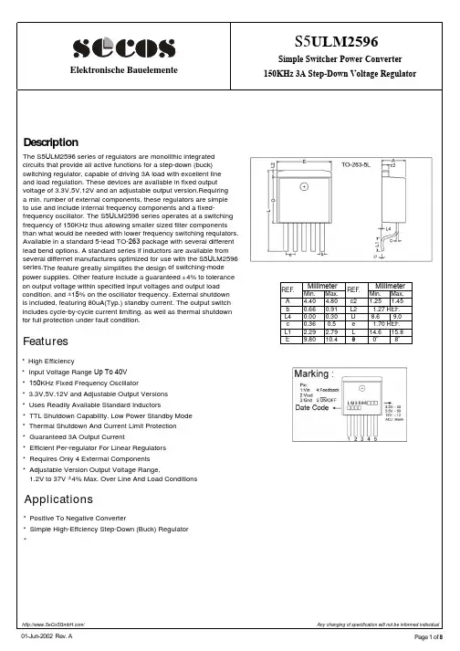
Elektronische Bauelemente01-Jun-2002 Rev. A Page 1 of 8REF . REF .MillimeterMillimeterElektronische BauelementePage 2 of 8Block DiagramFEEDBACKPin FunctionPIN#FUNCTION1 This is the positive input supply for the IC switching regulator. A suitable input must be present at this pin to minimize voltage transients and to supply the switching needed by regulator.2 Internal switch. The voltage at this pin switches between (+V IN – V SAT ) and approximately -0.5V, with a duty cycle of approximately V OUT /V IN . To minimize coupling to sensitive circuit, the PC board copper area connected to this pin should be keep to a minimum.3 Circuit ground4Senses the regulated output voltage to complete the feedback loop12VUnregulated680332201N5824680S5ULM2596-5.0 DC InputPage 3 of 801-Jun-2002 Rev. A Page 4 of 8Normalized Output Voltage Line RegulatorEfficiency Switch Saturation VoltageSwitch Current Limit Dropout Voltage/ Any changing of specification will not be informed individual 01-Jun-2002 Rev. A Page 5 of 8Elektronische BauelementeOperating Quiescent Current Shutdown Quiescent Current Minimum Operating Supply Voltage ON/OFF Threshold VoltageON/OFF Pin Current (Sinking)Switching Frequency/ Any changing of specification will not be informed individual 01-Jun-2002 Rev. A Page 6 of 801-Jun-2002 Rev. A Page 7 of 8tp:/// Any changing of specification will not be informed individual Elektronische BauelementeFeedback Pin BiasContinuous Mode Switching Waveforms Horizontal Time Base: 2 sDiscontinuous Mode Switching Waveforms Horizontal Time Base: 2 sLoad Transient Response for Continuous Mode100 sHorizontal Time Base: 200 s /dLoad Transient Response for Discontinuous Mode Horizontal Time Base:01-Jun-2002 Rev. A Page 8 of 8Elektronische BauelementeV out=VREF*(1+R2/R1) Where VREF=1.23V R2=R1*(Vout/VREF-1)Select R1 to be approximately 1k , use a 1% resistor for best stability. Cin-- 470uF, 50V , Aluminum Electrolytic Cout-- 220uF, 35V Aluminum Electrolytic D1-- 5A, 40V Schottky Rectifer, 1N5825 L1-- 68uH Figure 2 Standard Test Circuits and Layout GuidesCin-- 470uF, 50V , Aluminum Electrolytic Cout-- 220uF, 25V Aluminum Electrolytic D1-- 5A, 40V Schottky Rectifer, 1N5825 L1-- 68uHS5ELM2596。
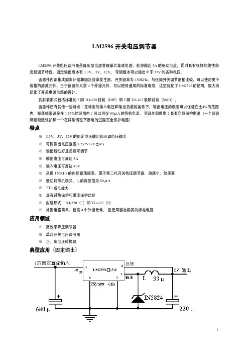
LM2596 开关电压调节器LM2596-ADJ 是3A 电流输出降压开关型集成稳压芯片 ,它内含固定频率振荡器(150KHZ ),和基准稳压器(1.23v ),并具有完善的保护电路:电流限制、热关断电路等。
利用该器件只需极少的外围器件便可构成高效稳压电路。
该器件还有其他一些特点:在特定的输入电压和输出负载的条件下,输出电压的误差可以保证在±4%的范围内,振荡频率误差在±15%的范围内;可以用仅 80μA 的待机电流, 实现外部断电;具有自我保护电路(一个两级降频限流保护和一个在异常情况下断电的过温完全保护电路)可调输出调节器的设计步骤条件:VOUT 为可调节的输出电压,VIN (max )为最大直流输入电压,ILOAD (max )为最大负载电流,F=开关频率(为固定值 150KHz )步骤:1. 输出电压值的计算(即选择图 1中的 R1和 R2)利用以下的公式来选择适当的电阻值,V out= Vref ( +1 )这里的 VREF=1.23V ,在 240Ω和 1.5KΩ之间为 R1 选择一个适当的阻值。
低阻值使敏感的反馈脚的噪声容限降到最小(选用精度为 1%金属膜电阻,可以使温度系数降低,随时间的稳定度最好)。
R2 = R1 ( — 1 )2. 电感的选择(L1)A. 可以通过以下的公式计算电感电压与微秒的乘积 E·T其中 VSAT 为内部开关饱和电压,且 VSAT=1.16VVD 为二极管正向压降,VD=0.5V 。
B. 用前面公式中所得的 E·T 的值,从图 7的纵坐标上找一个相匹配的电感序号。
在横坐标上选一个最大的负载电流。
C. 由 E·T 值和最大的负载电流值的交叉处确定一个电感区域,每个区域都由一个电感值和一个电感序号(LXX )表征。
D. 从图 8所列的 4个生产厂家的元件号中选一个适当的电感,最好使用磁屏蔽结构的电感器。
3. 输出电容的选择(COUT )A. 在大多数的使用中,使用 82μF ~820μF 之间的低等效电阻(Low ESR )的电解电容或固态钽电容效果最好,电容要靠近 IC ,管脚要短,连接的铜线要短。
LM2596全中文资料随着电子技术的发展,各种电子设备越来越多,而其中一个重要的电源管理模块就是开关电源。
在电子设备中,开关电源起着将交流电转换为直流电的作用,提供稳定可靠的电力供应。
而LM2596是一种常见的开关稳压模块,它被广泛应用于各种电子设备中,提供高效、稳定的电源管理解决方案。
LM2596是一款具有高效率、低功耗和稳定性的降压型开关稳压模块。
它能够将输入电压转换为相对稳定的输出电压,通常被用于降低电源电压供应至微控制器、电路板、传感器等部件。
同时,LM2596还具备短路保护、过热保护等功能,以确保电子设备的安全运行。
LM2596采用了开关型调制控制技术,能够在不同负载情况下自动调整开关频率和占空比,以保持输出电压稳定。
它的输入电压范围广,可以适应不同的电源输入,包括交流电和直流电。
而输出电压可通过外部电阻分压调整,从而满足不同电子设备的需求。
除了稳压功能,LM2596还具备过流保护功能。
当电流超过设定值时,它会自动切断输出,避免因电流过大而损坏电子设备。
同时,LM2596还配备了过热保护功能,当温度超过一定范围时,它会自动降低工作频率或停止工作,以防止过热引起故障。
LM2596作为一种常见的开关稳压模块,其技术参数和应用案例都有详尽的中文资料可供参考。
对于初学者而言,这些资料不仅提供了LM2596的基本工作原理和使用方法,还介绍了它在各种电子设备中的具体应用场景和性能要求。
其中,电路图、元器件清单和详细的步骤说明,使得初学者能够更好地理解和使用LM2596。
此外,还有一些中文论坛和社区提供了关于LM2596的技术讨论和使用心得的帖子。
这些帖子通常包含了实际应用中遇到的问题和解决方案,对于学习和掌握LM2596的使用具有很大帮助。
在这些中文论坛中,你可以与其他电子爱好者交流经验,共同探讨LM2596的使用技巧。
综上所述,LM2596作为一种常见的开关稳压模块,提供了高效、稳定的电源管理解决方案。
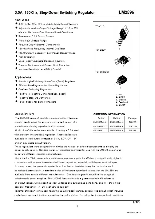
元器件交易网3.0A, 150Khz, Step-Down Switching RegulatorFEATURES3.3V, 5.0V, 12V, 15V, and Adjustable Output Versions Adjustable Version Output Voltage Range, 1.23 to 37V +/- 4%. Maximum Over Line and Load Conditions Guaranteed 3.0A Output Current Wide Input Voltage Range Requires Only 4 External Components 150Khz Fixed Frequency Internal Oscillator TTL Shutdown Capability, Low Power Standby Mode High Efficiency Uses Readily Available Standard Inductors Thermal Shutdown and Current Limit Protection Moisture Sensitivity Level(MSL) Equals1 TO-263(D2) TO-220V TO-220LM2596ApplicationsSimple High-Efficiency Step-Down(Buck) Regulator Efficient Pre-Regulator for Linear Regulators On-Card Switching Regulators Positive to Negative Converter(Buck-Boost) Negative Step-Up Converters Power Supply for Battery Chargers1. 2. 3. 4. 5. Vin Output Ground Feedback On/OffDESCRIPTIONThe LM2596 series of regulators are monolithic integrated circuits ideally suited for easy and convenient design of a step-down switching regualtor(buck converter). All circuits of this series are capable of driving a 3.0A load with excellent line and load regulation. These devices are available in fixed output voltages of 3.3V, 5.0V,12V, 15V, and an adjustable output version.ORDERING INFORMATIONDevice LM2596T-X.X LM2596TV-X.X LM2596R Marking LM2596T-X.X LM2596T-X.X LM2596R-X.X Package TO-220 TO-220V TO-263These regulatiors were designed to minimize the number of externalcomponents to simplify the power supply design. Standard series of inductors optimized for use with the LM2576 are offered by several different inductor manufacturers. Since the LM2596 converter is a switch-mode power supply, its efficiency is significantly higher in comparison with popular three-terminal limear reguators, especially with higher input voltages. In many cases, the power dissipated is so low that no heatsink is required or its size could be reduced dramatically. A standard series of inductors optimized for use with the LM2596 are available from several different manufacturers. This feature greatly simplifies the design of switch-mode power supplies. The LM2596 features include a guaranteed +/- 4% tolerance on output voltage within specified input voltages and output load conditions, and +/-15% on the oscillator frequency (+/- 2% over 0oC to 125 oC). External shutdown is included, featuring 80 uA(typical) standby current. The output switch includes cycle-bycycle current limiting, as well as thermal shutdown for full protection under fault conditions.HTC1Oct 2004 - Rev 0元器件交易网3.0A, 15V, Step-Down Switching RegulatorTypical Application (Fixed Output Voltage Versions)LM2596LM2596-5.033 uH680 uF1N5824220 uFFigure 1. Block Diagram and Typical ApplicationABSOLUTE MAXIMUM RATINGS(Absolute Maximum Ratings indicate limits beyond which damage to the device may occur.)Power DissipationTO-220, 5-LeadThermal Resistance, Junction-to-Ambient Thermal Resistance, Junction-to-caseTO-263Thermal Resistance, Junction-to-Ambient Thermal Resistance, Junction-to-caseHTC2Oct 2004 - Rev 0元器件交易网3.0A, 15V, Step-Down Switching RegulatorLM2596OPERATING RATINGS (Operating Ratings indicate conditions for which the device is intended to befunctional, but do not guarantee specific performance limits. For guaranteed specifications and test conditions, see the Electrical Characteristics.)ELECTRICAL CHARACTERISTICS / SYSTEM PARAMETERS ([Note 1] Test Circuit Figure 2) (Unless otherwise specified, Vin = 12 V for the 3.3 V, 5.0 V, and Adjustable version, Vin = 25 V for the 12 V version, and Vin = 30 V for the 15 V version. ILoad = 500 mA. For typical values TJ = 25°C, for min/max values TJ is the operating junction temperature range that applies [Note 2], unless otherwise noted.)LM2596-3.3 ([ Note 1]. Test Circuit Figure 2 )73 LM2596-5.0 ([ Note 1]. Test Circuit Figure 2 ) 180 LM2596-12 ([ Note 1]. Test Circuit Figure 2 )90 LM2596-15 ([ Note 1]. Test Circuit Figure 2 )98 LM2596-ADJ ([ Note 1]. Test Circuit Figure 2 )73HTC3Oct 2004 - Rev 0元器件交易网3.0A, 15V, Step-Down Switching RegulatorELECTRICAL CHARACTERISTICS / Device ParametersLM2596(Unless otherwise specified, Vin = 12 V for the 3.3 V, 5.0 V, and Adjustable version, Vin = 25 V for the 12 V version, and Vin = 30 V for the 15 V version. ILoad = 500 mA. For typical values Tj = 25°C, for min/max values Tj is the operating junction temperature range that applies [Note 2], unless otherwise noted.)10 0 127 110 15050 100 173 1731.16 01.4 1.53.6 3.4100 4.5 6.9 7.5 50 30 1002 5 00 2 0 2.0 2.0 2 V LOGIC = 2.5V (Regulator OFF) V LOGIC = 0.5V (Regulator ON) 5 0.02 1.3 1.32500.6 0.6 15 5.001. External components such as the catch diode, inductor, input and output capacitors can affect switching regulator system performance. When the LM2596 is used as shown in the Figure 1 test circuit, system performance will be as shown in system parameters section . 2. Tested junction temperature range for the LM2596 : TLOW = –0°C THIGH = +125°C 3. The oscillator frequency reduces to approximately 18 kHz in the event of an output short or an overload which causes the regulated output voltage to drop approximately 40% from the nominal output voltage. This self protection feature lowers the average dissipation of the IC by lowering the minimum duty cycle from 5% down to approximately 2%. 4. Output (Pin 2) sourcing current. No diode, inductor or capacitor connected to output pin. 5. Feedback (Pin 4) removed from output and connected to 0 V. 6. Feedback (Pin 4) removed from output and connected to +12 V for the Adjustable, 3.3 V, and 5.0V ersions, and +25 V for the 12 V and15 V versions, to force the output transistor “off”. 7. Vin = 40 V.HTC4Oct 2004 - Rev 0元器件交易网3.0A, 15V, Step-Down Switching RegulatorTYPICAL PERFORMANCE CHARACTERISTICS (Circuit of Figure 2)LM2596HTC5Oct 2004 - Rev 0元器件交易网3.0A, 15V, Step-Down Switching RegulatorTYPICAL PERFORMANCE CHARACTERISTICS (Circuit of Figure 2)Feedback Pin Bias CurrentLM2596HTC6Oct 2004 - Rev 0元器件交易网3.0A, 15V, Step-Down Switching RegulatorTest Circuit and Layout GuidelinesLM2596Figure 2. Typical Test Circuits and Layout GuideAs in any switching regulator, layout is very important. Rapidly switching currents associated with wiring inductance can generate voltage transients which can cause problems. For minimal inductance and ground loops, the wires indicated by heavy lines should be wide printed circuit traces and should be kept as short as possible. For best results, external components should be located as close to the switcher lC as possible using ground plane construction or single point grounding. If open core inductors are used, special care must be taken as to the location and positioning of this type of inductor. Allowing the inductor flux to intersect sensitive feedback, lC groundpath and COUT wiring can cause problems. When using the adjustable version, special care must be taken as to the location of the feedback resistors and the associated wiring. Physically locate both resistors near the IC, and route the wiring away from the inductor, especially an open core type of inductor.HTC7Oct 2004 - Rev 0元器件交易网3.0A, 15V, Step-Down Switching RegulatorLM2596PIN FUNCTION DESCRIPTION Symbol 1VinDescription This pin is the positive input supply for the LM2596 step–down switching23 45regulator.In order to minimize voltage transients and to supply the switching currents needed by the regulator, a suitable input bypass capacitor must be present .(Cin in Figure 1). Output This is the emitter of the internal switch. The saturation voltage Vsat of this output switch is typically 1.5 V. It should be kept in mind that the PCB area connected to this pin should be kept to a minimum in order to minimize coupling to sensitive circuitry. Circuit ground pin. See the information about the printed circuit board layout. Gnd Feedback This pin senses regulated output voltage to complete the feedback loop. The signal is divided by the internal resistor divider network R2, R1 and applied to the non–inverting input of the internal error amplifier. In the Adjustable version of the LM2596 switching regulator this pin is the direct input of the error amplifier and the resistor network R2, R1 is connected externally to allow programming of the output voltage. ON/OFF It allows the switching regulator circuit to be shut down using logic level signals, thus dropping the total input supply current to approximately 80 mA. The threshold voltage is typically 1.4 V. Applying a voltage above this value (up to +Vin) shuts the regulator off. If the voltage applied to this pin is lower than 1.4V or if this pin is left open, the regulator will be in the "on" conditionHTC8Oct 2004 - Rev 0元器件交易网3.0A, 15V, Step-Down Switching RegulatorLM2596PACKAGES DIMENSION : TO220-5LHTC9Oct 2004 - Rev 0元器件交易网3.0A, 15V, Step-Down Switching RegulatorPACKAGES DIMENSION : TO220V-5LLM2596HTC10Oct 2004 - Rev 0元器件交易网3.0A, 15V, Step-Down Switching RegulatorLM2596PACKAGES DIMENSION : TO263-5LHTC11Oct 2004 - Rev 0。
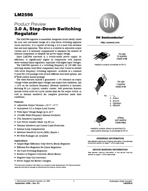
LM2596Product Preview3.0 A, Step-Down Switching RegulatorThe LM2596 regulator is monolithic integrated circuit ideally suited for easy and convenient design of a step−down switching regulator (buck converter). It is capable of driving a 3.0 A load with excellent line and load regulation. This device is available in adjustable output version and it is internally compensated to minimize the number of external components to simplify the power supply design.Since LM2596 converter is a switch−mode power supply, its efficiency is significantly higher in comparison with popular three−terminal linear regulators, especially with higher input voltages. The LM2596 operates at a switching frequency of 150 kHz thus allowing smaller sized filter components than what would be needed with lower frequency switching regulators. Available in a standard 5−lead TO−220 package with several different lead bend options, and D2PAK surface mount package.The other features include a guaranteed $4% tolerance on output voltage within specified input voltages and output load conditions, and $15% on the oscillator frequency. External shutdown is included, featuring 80 m A (typical) standby current. Self protection features include switch cycle−by−cycle current limit for the output switch, as well as thermal shutdown for complete protection under fault conditions.Features•Adjustable Output Versions 1.23 V − 37 V •Guaranteed 3.0 A Output Load Current•Wide Input V oltage Range up to 40 V•150 kHz Fixed Frequency Internal Oscillator•TTL Shutdown Capability•Low Power Standby Mode, typ 80 m A•Thermal Shutdown and Current Limit Protection •Internal Loop Compensation•Moisture Sensitivity Level (MSL) Equals 1•Pb−Free Packages are AvailableApplications•Simple High−Efficiency Step−Down (Buck) Regulator •Efficient Pre−Regulator for Linear Regulators•On−Card Switching Regulators•Positive to Negative Converter (Buck−Boost)•Negative Step−Up Converters•Power Supply for Battery ChargersThis document contains information on a product under development. ON Semiconductor reserves the right to change or discontinue this product without notice.See detailed ordering and shipping information in the package dimensions section on page 11 of this data sheet.ORDERING INFORMATIONTO−220TV SUFFIXCASE 314BHeatsink surface connected to Pin 3TO−220T SUFFIXCASE 314DPin 1.V in2.Output3.Ground4.Feedback5.ON/OFFD2PAKD2T SUFFIXCASE 936A Heatsink surface (shown as terminal 6 incase outline drawing) is connected to Pin 35See general marking information in the device marking section on page 11 of this data sheet.DEVICE MARKING INFORMATIONFigure 1. Block Diagram and Typical Application8.0 V - 40 V Unregulated DC InputTypical Application (Adjustable Output Voltage Versions)Representative Block Diagram and Typical ApplicationMAXIMUM RATINGSRatingSymbol Value Unit Maximum Supply Voltage V in 45V ON/OFF Pin Input Voltage−−0.3 V ≤ V ≤ +V inV Output Voltage to Ground (Steady −State)−−1.0VPower DissipationCase 314B and 314D (TO −220, 5−Lead)P D Internally LimitedW Thermal Resistance, Junction −to −Ambient R q JA 65°C/W Thermal Resistance, Junction −to −Case R q JC 5.0°C/W Case 936A (D 2PAK)P D Internally LimitedW Thermal Resistance, Junction −to −Ambient R q JA 70°C/W Thermal Resistance, Junction −to −Case R q JC 5.0°C/W Storage Temperature RangeT stg −65 to +150°C Minimum ESD Rating (Human Body Model: C = 100 pF, R = 1.5 k W )− 2.0kV Lead Temperature (Soldering, 10 seconds)−260°C Maximum Junction TemperatureT J150°CStresses exceeding Maximum Ratings may damage the device. Maximum Ratings are stress ratings only. Functional operation above the Recommended Operating Conditions is not implied. Extended exposure to stresses above the Recommended Operating Conditions may affect device reliability.PIN FUNCTION DESCRIPTIONPin Symbol Description (Refer to Figure 1)1V in This pin is the positive input supply for the LM2596 step−down switching regulator. In order to minimize voltage tran-sients and to supply the switching currents needed by the regulator, a suitable input bypass capacitor must bepresent (C in in Figure 1).2Output This is the emitter of the internal switch. The saturation voltage V sat of this output switch is typically 1.5 V. It should be kept in mind that the PCB area connected to this pin should be kept to a minimum in order to minimize coupling tosensitive circuitry.3GND Circuit ground pin. See the information about the printed circuit board layout.4Feedback This pin is the direct input of the error amplifier and the resistor network R2, R1 is connected externally to allow pro-gramming of the output voltage.5ON/OFF It allows the switching regulator circuit to be shut down using logic level signals, thus dropping the total input supply current to approximately 80 m A. The threshold voltage is typically 1.4 V. Applying a voltage above this value (up to+V in) shuts the regulator off. If the voltage applied to this pin is lower than 1.4 V or if this pin is left open, the regulatorwill be in the “on” condition.OPERATING RATINGS (Operating Ratings indicate conditions for which the device is intended to be functional, but do not guarantee specific performance limits. For guaranteed specifications and test conditions, see the Electrical Characteristics.)Rating Symbol Value Unit Operating Junction Temperature Range T J−40 to +125°C Supply Voltage V in 4.5 to 40VSYSTEM PARAMETERSELECTRICAL CHARACTERISTICS Specifications with standard type face are for T J = 25°C, and those with boldface type apply over full Operating Temperature Range −40°C to +125°CCharacteristics Symbol Min Typ Max Unit LM2596 (Note 1, Test Circuit Figure )Feedback Voltage (V in= 12 V, I Load = 0.5 A, V out = 5.0 V, )V FB 1.217 1.23 1.243VFeedback Voltage (8.0 V ≤ V in≤ 40 V, 0.5 A ≤ I Load≤ 3.0 A, V out = 5.0 V)V FB 1.1931.181.2671.28VEfficiency (V in= 12 V, I Load = 3.0 A, V out = 5.0 V)η−73−% Characteristics Symbol Min Typ Max Unit Feedback Bias Current (V out = 5.0 V)I b25100200nAOscillator Frequency( Note 2)f osc135120150165180kHzSaturation Voltage (I out = 3.0 A, Notes 3 and 4)V sat 1.5 1.82.0V Max Duty Cycle (ON) Note 4DC95%Current Limit (Peak Current Notes 2 and 3)I CL 4.23.55.6 6.97.5AOutput Leakage Current (Notes 5 and 6) Output = 0 VOutput = −1.0 V I L0.56.02.020mAQuiescent Current (Note 5)I Q 5.010mAStandby Quiescent Current (ON/OFF Pin = 5.0 V (“off”)) (Note 6)I stby50200250m AON/OFF PIN LOGIC INPUTThreshold Voltage 1.6VV out = 0 V (Regulator OFF)V IH 2.22.4VV out = Nominal Output Voltage (Regulator ON)V IL 1.00.8V ON/OFF Pin Input CurrentON/OFF Pin = 5.0 V (Regulator OFF)I IH−1530m A ON/OFF Pin = 0 V (regulator ON)I IL−0.01 5.0m A 1.External components such as the catch diode, inductor, input and output capacitors can affect switching regulator system performance.When the LM2596 is used as shown in the Figure 15test circuit, system performance will be as shown in system parameters section.2.The oscillator frequency reduces to approximately 30 kHz in the event of an output short or an overload which causes the regulated outputvoltage to drop approximately 40% from the nominal output voltage. This self protection feature lowers the average dissipation of the IC by lowering the minimum duty cycle from 5% down to approximately 2%.3.No diode, inductor or capacitor connected to output pin.4.Feedback (Pin 4) removed from output and connected to 0 V.5.Feedback (Pin 4) removed from output and connected to +12 V to force the output transistor “off”.6.V in = 40 V.I Q , Q U I E S C E N T C U R R E N T (m A )V o u t , O U T P U T V O L T A G E C H A N G E (%)V o u t , O U T P U T V O L T A G E C H A N G E (%), S T A N D B Y Q U I E S C E N T C U R R E N T (T J , JUNCTION TEMPERATURE (°C)I O , O U T P U T C U R R E N T (A )T J , JUNCTION TEMPERATURE (°C)V in , INPUT VOLTAGE (V)V in , INPUT VOLTAGE (V)I N P U T - O U T P U T D I F F E R E N T I A L (V )T J , JUNCTION TEMPERATURE (°C)Figure 2. Normalized Output Voltage T J , JUNCTION TEMPERATURE (°C)Figure 3. Line RegulationFigure 4. Dropout Voltage Figure 5. Current LimitFigure 6. Quiescent Current Figure 7. Standby Quiescent CurrentμA )1.00.60.20-0.2-0.4-1.0 1.41.21.00.80.60.40.20-0.2-0.4-0.66.56.05.55.04.54.02018161412108.06.04.0-0.8-0.60.40.8I s t b yV s a t , S A T U R A T I O N V O L T A G E (V )2.02.53.04.0I b , F E E D B A C K P I N C U R R E N T (n A ), S T A N D B Y Q U I E S C E N T C U R R E N T (μA )I s t b y , I N P U T V O L T A G E (V )T J , JUNCTION TEMPERATURE (°C)SWITCH CURRENT (A)N O R M A L I Z E D F R E Q U E N C Y (%)T J , JUNCTION TEMPERATURE (°C)Figure 8. Standby Quiescent Current V in , INPUT VOLTAGE (V)Figure 9. Switch Saturation VoltageFigure 10. Oscillator FrequencyFigure 11. Minimum Operating VoltageFigure 12. Feedback Pin Current2001801401201008060402001.61.41.21.00.80.60.40.205.04.53.51.51.00.50-50T J , JUNCTION TEMPERATURE (°C)100806040200-20-40-60-80-100125100755025-25-50160V i n −9.0−8.0−7.0−6.0−5.0−4.0−3.0−2.0−1.00.01.0−2.0 A 00ABC 100 m s/DIV2 m s/DIVFigure 13. Switching WaveformsFigure 14. Load Transient ResponseVout = 15 VA: Output Pin Voltage, 10 V/DIV B: Inductor Current, 2.0 A/DIVC: Inductor Current, 2.0 A/DIV, AC −CoupledD: Output Ripple Voltage, 50 mV/dDIV, AC −Coupled Horizontal Time Base: 5.0 m s/DIV50 V 04.0 A 2.0 A 100 mV OutputVoltageChange03.0 A2.0 A 1.0 A4.0 A - 100 mVLoad CurrentDFigure 15. Typical Test CircuitAdjustable Output Voltage Versionsout ref R2R1ǓR2+R1ǒV out V ref 1.0ǓWhere V ref = 1.23 V, R1 between 1.0 k and 5.0 kPCB LAYOUT GUIDELINESAs in any switching regulator, the layout of the printed circuit board is very important. Rapidly switching currents associated with wiring inductance, stray capacitance and parasitic inductance of the printed circuit board traces can generate voltage transients which can generate electromagnetic interferences (EMI) and affect the desired operation. As indicated in the Figure 15, to minimize inductance and ground loops, the length of the leads indicated by heavy lines should be kept as short as possible.For best results, single −point grounding (as indicated) or ground plane construction should be used.On the other hand, the PCB area connected to the Pin 2(emitter of the internal switch) of the LM2596 should be kept to a minimum in order to minimize coupling to sensitive circuitry.Another sensitive part of the circuit is the feedback. It is important to keep the sensitive feedback wiring short. To assure this, physically locate the programming resistors near to the regulator, when using the adjustable version of the LM2596 regulator.DESIGN PROCEDUREBuck Converter BasicsThe LM2596 is a “Buck” or Step −Down Converter which is the most elementary forward −mode converter. Its basic schematic can be seen in Figure 16.The operation of this regulator topology has two distinct time periods. The first one occurs when the series switch is on, the input voltage is connected to the input of the inductor.The output of the inductor is the output voltage, and the rectifier (or catch diode) is reverse biased. During this period, since there is a constant voltage source connected across the inductor, the inductor current begins to linearly ramp upwards, as described by the following equation:I L(on)+ǒV IN *V OUT Ǔt onLDuring this “on” period, energy is stored within the core material in the form of magnetic flux. If the inductor is properly designed, there is sufficient energy stored to carry the requirements of the load during the “off” period.Figure 16. Basic Buck ConverterR LoadPower The next period is the “off” period of the power switch.When the power switch turns off, the voltage across the inductor reverses its polarity and is clamped at one diode voltage drop below ground by the catch diode. The current now flows through the catch diode thus maintaining the load current loop. This removes the stored energy from the inductor. The inductor current during this time is:I L(off)+ǒV OUT *V D Ǔt offLThis period ends when the power switch is once again turned on. Regulation of the converter is accomplished by varying the duty cycle of the power switch. It is possible to describe the duty cycle as follows:d +ton T, where T is the period of switching.For the buck converter with ideal components, the duty cycle can also be described as:d +V outV inFigure 17 shows the buck converter, idealized waveforms of the catch diode voltage and the inductor current.Figure 17. Buck Converter Idealized WaveformsPROCEDURE (ADJUSTABLE OUTPUT VERSION:LM2596)PROCEDURE (ADJUSTABLE OUTPUT VERSION:LM2596) (CONTINUED)ORDERING INFORMATIONDevicePackage Shipping †LM2596TADJG TO −220(Pb −Free)50 Units / Rail LM2596TVADJG TO −220 (F)(Pb −Free)50 Units / Rail LM2596DSADJG D 2PAK (Pb −Free)50 Units / Rail LM2596DSADJR4GD 2PAK (Pb −Free)2500 / Tape & Reel†For information on tape and reel specifications, including part orientation and tape sizes, please refer to our Tape and Reel Packaging Specifications Brochure, BRD8011/D.A = Assembly Location WL = Wafer Lot Y = YearWW = Work WeekG= Pb −Free PackageTO −220TV SUFFIX CASE 314B1MARKING DIAGRAMS5TO −220T SUFFIX CASE 314DD 2PAK D2T SUFFIX CASE 936ALM2596T −ADJ AWLYWWGLM2596T −ADJ AWLYWWGLM2596D2T −ADJ AWLYWWG1515LM2596−ADJ AWLYWWG 15TO −220TV SUFFIX CASE 314B −05ISSUE LM0.10 (0.254)PMT NOTES:1.DIMENSIONING AND TOLERANCING PER ANSI Y14.5M, 1982.2.CONTROLLING DIMENSION: INCH.3.DIMENSION D DOES NOT INCLUDEINTERCONNECT BAR (DAMBAR) PROTRUSION.DIMENSION D INCLUDING PROTRUSION SHALL NOT EXCEED 0.043 (1.092) MAXIMUM.DIM MIN MAX MIN MAX MILLIMETERSINCHES A 0.5720.61314.52915.570B 0.3900.4159.90610.541C 0.1700.180 4.318 4.572D 0.0250.0380.6350.965E 0.0480.055 1.219 1.397F 0.8500.93521.59023.749G 0.067 BSC 1.702 BSC H 0.166 BSC 4.216 BSC J 0.0150.0250.3810.635K 0.900 1.10022.86027.940L 0.3200.3658.1289.271N 0.320 BSC 8.128 BSC Q 0.1400.153 3.556 3.886S ---0.620---15.748U 0.4680.50511.88812.827V ---0.735---18.669W0.0900.1102.286 2.794TO −220T SUFFIX CASE 314D −04ISSUE FMQM0.356 (0.014)T SEATING PLANEDIM MIN MAX MIN MAX MILLIMETERSINCHES A 0.5720.61314.52915.570B 0.3900.4159.90610.541C 0.1700.180 4.318 4.572D 0.0250.0380.6350.965E 0.0480.055 1.219 1.397G 0.067 BSC 1.702 BSC H 0.0870.112 2.210 2.845J 0.0150.0250.3810.635K 0.977 1.04524.81026.543L 0.3200.3658.1289.271Q 0.1400.153 3.556 3.886U0.1050.1172.667 2.972NOTES:1.DIMENSIONING AND TOLERANCING PER ANSI Y14.5M, 1982.2.CONTROLLING DIMENSION: INCH.3.DIMENSION D DOES NOT INCLUDEINTERCONNECT BAR (DAMBAR) PROTRUSION.DIMENSION D INCLUDING PROTRUSION SHALL NOT EXCEED 10.92 (0.043) MAXIMUM.B10.3750.4159.52510.541DETAIL A −AD 2PAK D2T SUFFIX CASE 936A −02ISSUE C5 REF NOTES:1.DIMENSIONING AND TOLERANCING PER ANSI Y14.5M, 1982.2.CONTROLLING DIMENSION: INCH.3.TAB CONTOUR OPTIONAL WITHIN DIMENSIONS A AND K.4.DIMENSIONS U AND V ESTABLISH A MINIMUM MOUNTING SURFACE FOR TERMINAL 6.5.DIMENSIONS A AND B DO NOT INCLUDE MOLD FLASH OR GATE PROTRUSIONS. MOLD FLASH AND GATE PROTRUSIONS NOT TO EXCEED 0.025(0.635) MAXIMUM.DIM A MIN MAX MIN MAX MILLIMETERS 0.3860.4039.80410.236INCHES B 0.3560.3689.0429.347C 0.1700.180 4.318 4.572D 0.0260.0360.6600.914E 0.0450.055 1.143 1.397G 0.067 BSC 1.702 BSC H 0.5390.57913.69114.707K 0.050 REF 1.270 REF L 0.0000.0100.0000.254M 0.0880.102 2.235 2.591N 0.0180.0260.4570.660P 0.0580.0781.473 1.981R 5 REF S 0.116 REF 2.946 REF U 0.200 MIN 5.080 MIN V0.250 MIN6.350 MIN__SCALE 3:1ǒmm inchesǓ*For additional information on our Pb −Free strategy and solderingdetails, please download the ON Semiconductor Soldering and Mounting Techniques Reference Manual, SOLDERRM/D.ON Semiconductor and are registered trademarks of Semiconductor Components Industries, LLC (SCILLC). SCILLC reserves the right to make changes without further notice to any products herein. SCILLC makes no warranty, representation or guarantee regarding the suitability of its products for any particular purpose, nor does SCILLC assume any liability arising out of the application or use of any product or circuit, and specifically disclaims any and all liability, including without limitation special, consequential or incidental damages.“Typical” parameters which may be provided in SCILLC data sheets and/or specifications can and do vary in different applications and actual performance may vary over time. All operating parameters, including “Typicals” must be validated for each customer application by customer’s technical experts. SCILLC does not convey any license under its patent rights nor the rights of others. SCILLC products are not designed, intended, or authorized for use as components in systems intended for surgical implant into the body, or other applications intended to support or sustain life, or for any other application in which the failure of the SCILLC product could create a situation where personal injury or death may occur.Should Buyer purchase or use SCILLC products for any such unintended or unauthorized application, Buyer shall indemnify and hold SCILLC and its officers, employees, subsidiaries,affiliates, and distributors harmless against all claims, costs, damages, and expenses, and reasonable attorney fees arising out of, directly or indirectly, any claim of personal injury or death associated with such unintended or unauthorized use, even if such claim alleges that SCILLC was negligent regarding the design or manufacture of the part. SCILLC is an Equal Opportunity/Affirmative Action Employer. This literature is subject to all applicable copyright laws and is not for resale in any manner.PUBLICATION ORDERING INFORMATION。
LM2596稳压模块产品使用手册
【简要说明】
一、尺寸:长72mmX宽40mmX高18mm
二、主要芯片:整流桥、LM2596
三、工作电压:输入电压小于42V,输出电压 5V 另有12V,3.3V可选。
四、特点:1、具有输出电压指示灯。
2、最大输出电流3A。
3、采用螺旋压接端子。
4、强大的滤波电路。
5、输出转换效率高。
6、固定频率振荡器(150KHZ)
7、具有完善的保护电路:电流限制、热关断电路等
8、只需极少的外围器件
9、转换效率75%~88%
10、工作温度范围-40℃~+125℃
11、工作湿度 40% ~ 80%RH
12、输出电压的误差可以保证在±4%的范围内。
LM2596芯片说明:
【标注说明】
【功能描述】
【原理图】
【PCB图】
【元件清单】
【应用举例1】
【应用举例2】
【图片展示】。
lm2596中文资料1. 概述lm2596是一款高效率开关电源稳压器芯片,广泛应用于电子设备中对直流电压进行稳定调整的场合。
本文档将详细介绍lm2596的特性、工作原理、应用场景以及使用注意事项。
2. 特性•宽输入电压范围:4V-40V•可调输出电压范围:1.23V-37V•高效率:可达到92%•最大输出电流:3A•过热保护功能3. 工作原理lm2596采用了开关稳压器的工作原理,通过周期性地开关和断开电流流通路径,将输入电压转换为稳定的输出电压。
其主要原理如下:1.输入电压通过电感和开关管传导到输出端,同时电容储存能量。
2.控制器检测输出电压,如果低于设定值,则控制开关管开启,使电流通过电感传输到输出端,提供稳定的输出电压。
3.如果输出电压高于设定值,则控制开关管关闭,切断电流流动。
这种周期性的开关和断开电路,可以通过控制开关管的开启时间和关闭时间,来调整输出电压的稳定性和精确度。
4. 应用场景lm2596广泛应用于各种需要稳定直流电压的场合,以下是lm2596常见的应用场景:4.1 电子设备稳压电源lm2596可以根据需要调整输出电压,可以在电子设备中作为稳压电源芯片使用。
它可以将输入电压调整为稳定的输出电压,以供电子设备正常运行。
4.2 LED照明由于lm2596具有高效率和可调输出电压的特性,非常适合用于LED照明应用。
lm2596可以将输入电压调整为适合LED灯的电压,提供稳定的电源以驱动LED照明。
4.3 高频电源lm2596的高效率和宽输入电压范围,使其非常适合用于高频电源应用。
lm2596可以将输入电压转换为稳定的高频输出,满足高频电源的需求。
5. 使用注意事项在使用lm2596时,请注意以下事项:1.输入电压不要超过40V,否则可能导致芯片过载损坏。
2.充分考虑散热问题,尽量避免芯片过热,建议在芯片周围预留散热空间。
3.在使用lm2596时,应按照芯片的使用说明进行正确的电路设计和连接。
LM2596集成稳压芯片的基本特性及应用LM2596系列是德州仪器(TI)生产的3A电流输出降压开关型集成稳压芯片,它内含固定频率振荡器(150KHZ)和基准稳压器(1.23v),并具有完善的保护电路、电流限制、热关断电路等。
利用该器件只需极少的外围器件便可构成高效稳压电路。
提供的有:3.3V、5V、12V及可调(-ADJ)等多个电压档次产品。
LM2596内部包含150KHZ振荡器、1.23v基准稳压电路、热关断电路、电流限制电路、放大器、比较器和内部稳压电路等。
该器件内部集成频率补偿和固定频率发生器,开关频率为150KHz,与低频开关调节器相比较,可以使用更小规格的滤波元件。
由于该器件只需4个外接元件,可以使用通用的标准电感,这更优化了LM2596的使用,极大地简化了开关电源电路的设计。
其封装形式包括标准的5脚TO-220封装(DIP)和5脚TO-263表贴封装(SMD)。
该器件还有其他一些特点:在特定的输入电压和输出负载的条件下,输出电压的误差可以保证在±4%的范围内,振荡频率误差在±15%的范围内;可以用仅80μA的待机电流,实现外部断电;具有自我保护电路(一个两级降频限流保护和一个在异常情况下断电的过温完全保护电路)特性如下:1、输出电压:3.3V、5V、12V及(ADJ)等,最大输出电压37V2、工作模式:低功耗/正常两种模式。
可外部控制3、工作模式控制:TTL电平相容4、所需外部组件:仅四个(不可调);六个(可调)5、器件保护:热关断及电流限制6、封装形式:5脚(TO-220(T);TO-263(S))应用领域:1、高效率降压调节器2、单片开关电压调节器3、正、负电压转换器推荐阅读:http:///yuanqijian/bianyaqi/20180124622112l。
元器件交易网3.0A, 150Khz, Step-Down Switching RegulatorFEATURES3.3V, 5.0V, 12V, 15V, and Adjustable Output Versions Adjustable Version Output Voltage Range, 1.23 to 37V +/- 4%. Maximum Over Line and Load Conditions Guaranteed 3.0A Output Current Wide Input Voltage Range Requires Only 4 External Components 150Khz Fixed Frequency Internal Oscillator TTL Shutdown Capability, Low Power Standby Mode High Efficiency Uses Readily Available Standard Inductors Thermal Shutdown and Current Limit Protection Moisture Sensitivity Level(MSL) Equals1 TO-263(D2) TO-220V TO-220LM2596ApplicationsSimple High-Efficiency Step-Down(Buck) Regulator Efficient Pre-Regulator for Linear Regulators On-Card Switching Regulators Positive to Negative Converter(Buck-Boost) Negative Step-Up Converters Power Supply for Battery Chargers1. 2. 3. 4. 5. Vin Output Ground Feedback On/OffDESCRIPTIONThe LM2596 series of regulators are monolithic integrated circuits ideally suited for easy and convenient design of a step-down switching regualtor(buck converter). All circuits of this series are capable of driving a 3.0A load with excellent line and load regulation. These devices are available in fixed output voltages of 3.3V, 5.0V,12V, 15V, and an adjustable output version.ORDERING INFORMATIONDevice LM2596T-X.X LM2596TV-X.X LM2596R Marking LM2596T-X.X LM2596T-X.X LM2596R-X.X Package TO-220 TO-220V TO-263These regulatiors were designed to minimize the number of externalcomponents to simplify the power supply design. Standard series of inductors optimized for use with the LM2576 are offered by several different inductor manufacturers. Since the LM2596 converter is a switch-mode power supply, its efficiency is significantly higher in comparison with popular three-terminal limear reguators, especially with higher input voltages. In many cases, the power dissipated is so low that no heatsink is required or its size could be reduced dramatically. A standard series of inductors optimized for use with the LM2596 are available from several different manufacturers. This feature greatly simplifies the design of switch-mode power supplies. The LM2596 features include a guaranteed +/- 4% tolerance on output voltage within specified input voltages and output load conditions, and +/-15% on the oscillator frequency (+/- 2% over 0oC to 125 oC). External shutdown is included, featuring 80 uA(typical) standby current. The output switch includes cycle-bycycle current limiting, as well as thermal shutdown for full protection under fault conditions.HTC1Oct 2004 - Rev 0元器件交易网3.0A, 15V, Step-Down Switching RegulatorTypical Application (Fixed Output Voltage Versions)LM2596LM2596-5.033 uH680 uF1N5824220 uFFigure 1. Block Diagram and Typical ApplicationABSOLUTE MAXIMUM RATINGS(Absolute Maximum Ratings indicate limits beyond which damage to the device may occur.)Power DissipationTO-220, 5-LeadThermal Resistance, Junction-to-Ambient Thermal Resistance, Junction-to-caseTO-263Thermal Resistance, Junction-to-Ambient Thermal Resistance, Junction-to-caseHTC2Oct 2004 - Rev 0元器件交易网3.0A, 15V, Step-Down Switching RegulatorLM2596OPERATING RATINGS (Operating Ratings indicate conditions for which the device is intended to befunctional, but do not guarantee specific performance limits. For guaranteed specifications and test conditions, see the Electrical Characteristics.)ELECTRICAL CHARACTERISTICS / SYSTEM PARAMETERS ([Note 1] Test Circuit Figure 2) (Unless otherwise specified, Vin = 12 V for the 3.3 V, 5.0 V, and Adjustable version, Vin = 25 V for the 12 V version, and Vin = 30 V for the 15 V version. ILoad = 500 mA. For typical values TJ = 25°C, for min/max values TJ is the operating junction temperature range that applies [Note 2], unless otherwise noted.)LM2596-3.3 ([ Note 1]. Test Circuit Figure 2 )73 LM2596-5.0 ([ Note 1]. Test Circuit Figure 2 ) 180 LM2596-12 ([ Note 1]. Test Circuit Figure 2 )90 LM2596-15 ([ Note 1]. Test Circuit Figure 2 )98 LM2596-ADJ ([ Note 1]. Test Circuit Figure 2 )73HTC3Oct 2004 - Rev 0元器件交易网3.0A, 15V, Step-Down Switching RegulatorELECTRICAL CHARACTERISTICS / Device ParametersLM2596(Unless otherwise specified, Vin = 12 V for the 3.3 V, 5.0 V, and Adjustable version, Vin = 25 V for the 12 V version, and Vin = 30 V for the 15 V version. ILoad = 500 mA. For typical values Tj = 25°C, for min/max values Tj is the operating junction temperature range that applies [Note 2], unless otherwise noted.)10 0 127 110 15050 100 173 1731.16 01.4 1.53.6 3.4100 4.5 6.9 7.5 50 30 1002 5 00 2 0 2.0 2.0 2 V LOGIC = 2.5V (Regulator OFF) V LOGIC = 0.5V (Regulator ON) 5 0.02 1.3 1.32500.6 0.6 15 5.001. External components such as the catch diode, inductor, input and output capacitors can affect switching regulator system performance. When the LM2596 is used as shown in the Figure 1 test circuit, system performance will be as shown in system parameters section . 2. Tested junction temperature range for the LM2596 : TLOW = –0°C THIGH = +125°C 3. The oscillator frequency reduces to approximately 18 kHz in the event of an output short or an overload which causes the regulated output voltage to drop approximately 40% from the nominal output voltage. This self protection feature lowers the average dissipation of the IC by lowering the minimum duty cycle from 5% down to approximately 2%. 4. Output (Pin 2) sourcing current. No diode, inductor or capacitor connected to output pin. 5. Feedback (Pin 4) removed from output and connected to 0 V. 6. Feedback (Pin 4) removed from output and connected to +12 V for the Adjustable, 3.3 V, and 5.0V ersions, and +25 V for the 12 V and15 V versions, to force the output transistor “off”. 7. Vin = 40 V.HTC4Oct 2004 - Rev 0元器件交易网3.0A, 15V, Step-Down Switching RegulatorTYPICAL PERFORMANCE CHARACTERISTICS (Circuit of Figure 2)LM2596HTC5Oct 2004 - Rev 0元器件交易网3.0A, 15V, Step-Down Switching RegulatorTYPICAL PERFORMANCE CHARACTERISTICS (Circuit of Figure 2)Feedback Pin Bias CurrentLM2596HTC6Oct 2004 - Rev 0元器件交易网3.0A, 15V, Step-Down Switching RegulatorTest Circuit and Layout GuidelinesLM2596Figure 2. Typical Test Circuits and Layout GuideAs in any switching regulator, layout is very important. Rapidly switching currents associated with wiring inductance can generate voltage transients which can cause problems. For minimal inductance and ground loops, the wires indicated by heavy lines should be wide printed circuit traces and should be kept as short as possible. For best results, external components should be located as close to the switcher lC as possible using ground plane construction or single point grounding. If open core inductors are used, special care must be taken as to the location and positioning of this type of inductor. Allowing the inductor flux to intersect sensitive feedback, lC groundpath and COUT wiring can cause problems. When using the adjustable version, special care must be taken as to the location of the feedback resistors and the associated wiring. Physically locate both resistors near the IC, and route the wiring away from the inductor, especially an open core type of inductor.HTC7Oct 2004 - Rev 0元器件交易网3.0A, 15V, Step-Down Switching RegulatorLM2596PIN FUNCTION DESCRIPTION Symbol 1VinDescription This pin is the positive input supply for the LM2596 step–down switching23 45regulator.In order to minimize voltage transients and to supply the switching currents needed by the regulator, a suitable input bypass capacitor must be present .(Cin in Figure 1). Output This is the emitter of the internal switch. The saturation voltage Vsat of this output switch is typically 1.5 V. It should be kept in mind that the PCB area connected to this pin should be kept to a minimum in order to minimize coupling to sensitive circuitry. Circuit ground pin. See the information about the printed circuit board layout. Gnd Feedback This pin senses regulated output voltage to complete the feedback loop. The signal is divided by the internal resistor divider network R2, R1 and applied to the non–inverting input of the internal error amplifier. In the Adjustable version of the LM2596 switching regulator this pin is the direct input of the error amplifier and the resistor network R2, R1 is connected externally to allow programming of the output voltage. ON/OFF It allows the switching regulator circuit to be shut down using logic level signals, thus dropping the total input supply current to approximately 80 mA. The threshold voltage is typically 1.4 V. Applying a voltage above this value (up to +Vin) shuts the regulator off. If the voltage applied to this pin is lower than 1.4V or if this pin is left open, the regulator will be in the "on" conditionHTC8Oct 2004 - Rev 0元器件交易网3.0A, 15V, Step-Down Switching RegulatorLM2596PACKAGES DIMENSION : TO220-5LHTC9Oct 2004 - Rev 0元器件交易网3.0A, 15V, Step-Down Switching RegulatorPACKAGES DIMENSION : TO220V-5LLM2596HTC10Oct 2004 - Rev 0元器件交易网3.0A, 15V, Step-Down Switching RegulatorLM2596PACKAGES DIMENSION : TO263-5LHTC11Oct 2004 - Rev 0。
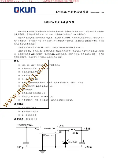
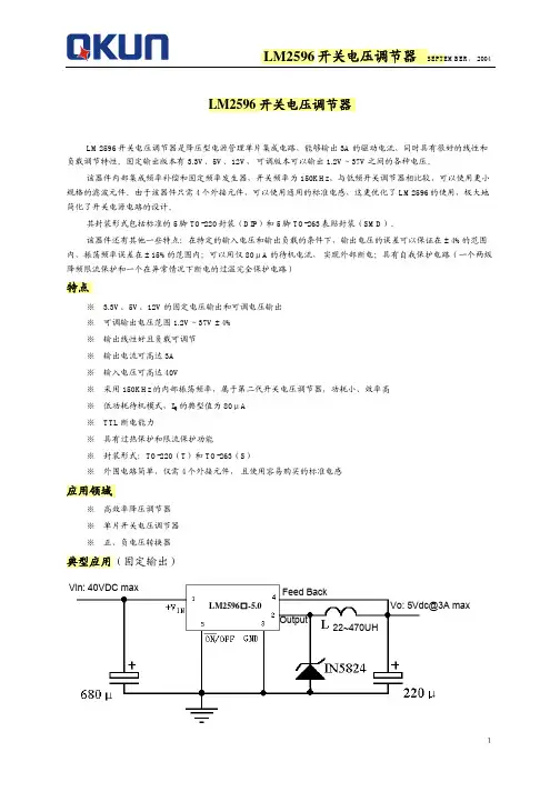
LM2596电源降压调整器(150KHz,3A)英文文章名:LM2596 SIMPLE SWITCHER® Power Converter 150 kHz3A Step-Down Voltage Regulator文章出处:版本号:DS012583 日期:2002年5月摘录人:黄明强摘录日期:2007年5月3日是否好买估计:生产中心正在使用价格:概述:LM2596系列开关电压调节器是降压型电源管理单片集成电路,能够输出3A的驱动电流,同时具有很好的线性和负载调节特性。
固定输出版本有3.3V、5V、12V,还有一个输出可调版本。
添加少量的外部元件就可以使用该电压调节器。
该器件内部集成有频率补偿和固定频率发生器。
开关频率为150KHz,与低频开关调节器相比较,可以使用更小规格的滤波元件。
其封装形式包括标准的5脚TO-220封装和5脚TO-263表贴封装。
由于该器件可以使用通用的标准电感,这更优化了LM2596的使用,极大地简化了开关电源电路的设计。
该器件还有其他一些特点:在特定的输入电压和输出负载的条件下,输出电压的误差可以保证在±4%的范围内,振荡频率误差在±15%的范围内;可以用仅80μA的待机电流,实现外部断电;具有自我保护电路(一个两级降频限流保护和一个在异常情况下断电的过温完全保护电路)。
特征:※ 3.3V、5V、12V的固定电压输出和可调电压输出※可调输出电压范围1.2V~37V,±4%※封装形式:TO-220(T)和TO-263(S)※保证输出负载电流3A※输入电压可高达40V※仅需4个外接元件※很好的线性和负载调节特性※150KHz固定频率的内部振荡器※TTL关断能力※低功耗待机模式,I Q的典型值为80μA※高转换效率※使用容易购买的标准电感※具有过热保护和限流保护功能应用:※简易高效率降压调节器※在卡上的开关电压调节器※正到负电压转换器专利号:5382918典型电路(固定输出电压版本):封装和型号:※弯曲交叉的引脚,通孔封装,5脚TO-220 (T)订货型号:LM2596T-3.3, LM2596T-5.0,LM2596T-12 or LM2596T-ADJ ※表面贴封装,5脚TO-263 (S)订货型号:LM2596S-3.3, LM2596S-5.0, LM2596S-12 or LM2596S-ADJ 极限条件:最大供电电压45VON /OFF 管脚输入电压-0.3≤V≤+25V反馈脚电压-0.3≤V≤+25V输出电压到地(稳态)-1V功率消耗内部限定储存温度-65°C 到+150°CESD易感性(人体模式)2KV焊接温度T封装(锡焊, 10秒) +260°C最大结温+150°C运行条件:温度范围-40°C≤T J≤+125°C供电电压 4.5V 到40VLM2596-3.3电参数说明:标准字体对应的项目适合于TJ=25℃时,粗体字对应的项目适合于全温度范围LM2596-5.0电参数说明:标准字体对应的项目适合于TJ=25℃时,粗体字对应的项目适合于全温度范围LM2596-12电参数所有输出电压版本电参数说明:标准字体对应的项目适合于TJ=25℃时,带下划线的粗斜体字对应的项目适合于整个温度范围。
开关型稳压芯片LM2576中文资料LM2576系列开关稳压集成电路是线性三端稳压器件(如78xx系列端稳压集成电路)的替代品,它具有可靠的工作性能、较高的工作效率和较强的输出电流驱动能力,从而为MCU的稳定、可靠工作提供了强有力的保证。
LM2576简介LM2576系列是美国国家半导体公司生产的3A电流输出降压开关型集成稳压电路,它内含固定频率振荡器(52kHz)和基准稳压器(1.23V),并具有完善的保护电路,包括电流限制及热关断电路等,利用该器件只需极少的外围器件便可构成高效稳压电路。
LM2576系列包括LM2576(最高输入电压40V)及LM2576HV(最高输入电压60V)二个系列。
各系列产品均提供有3.3V(-3.3)、5V(-5.0)、12V(-12)、15V(-15)及可调(-ADJ)等多个电压档次产品。
此外,该芯片还提供了工作状态的外部控制引脚。
LM2576系列开关稳压集成电路的主要特性如下[2]:●最大输出电流:3A;●最高输入电压:LM2576为40V,LM2576HV为60V;●输出电压:3.3V、5V、12V、15V和ADJ(可调)等可选;●振东频率:52kHz;●转换效率:75%~88%(不同电压输出时的效率不同);●控制方式:PWM;●工作温度范围:-40℃~+125℃●工作模式:低功耗/正常两种模式可外部控制;●工作模式控制:TTL电平兼容;●所需外部元件:仅四个(不可调)或六个(可调);●器件保护:热关断及电流限制;●封装形式:TO-220或TO-263。
LM2576的内部框图如图1所示,该框图的引脚定义对应于五脚TO-220封装形式。
LM2576内部包含52kHz振荡器、1.23V基准稳压电路、热关断电路、电流限制电路、放大器、比较器及内部稳压电路等。
为了产生不同的输出电压,通常将比较器的负端接基准电压(1.23V),正端接分压电阻网络,这样可根据输出电压的不同选定不同的阻值,其中R1=1kΩ(可调-ADJ时开路),R2分别为1.7 kΩ(3.3V)、3.1 kΩ(5V)、8.84 kΩ(12V)、11.3 kΩ(15V)和0(-ADJ),上述电阻依据型号不同已在芯片内部做了精确调整,因而无需使用者考虑。